

Page 1
查询LMC6442供应商
LMC6442
Dual Micropower Rail-to-Rail Output Single Supply
Operational Amplifier
LMC6442 Dual Micropower Rail-to-Rail Output Single Supply Operational Amplifier
September 1997
General Description
The LMC6442 is ideal for battery powered systems, where
very low supply current (less than one microamp per amplifier) and Rail-to-Rail output swing is required. It is characterized for 2.2V to 10V operation, and at 2.2V supply, the
LMC6442 is ideal for single (Li-Ion) or two cell (NiCad or alkaline) battery systems.
The LMC6442 is designed for battery powered systems that
require long service life through low supply current, such as
smoke and gas detectors, and pager or personal communications systems.
Operation from single supply is enhanced by the wide common mode input voltage range which includes the ground (or
negative supply) for ground sensing applications. Very low
(5fA, typical) input bias current and near constant supply current over supply voltage enhance the LMC6442’s performance near the end-of-life battery voltage.
Designed for closed loop gains of greater than plus two (or
minus one), the amplifier has typically 9.5 KHz GBWP (Gain
Bandwidth Product). Unity gain can be used with a simple
compensation circuit, which also allows capacitive loads of
up to 300 pF to be driven, as described in the Application
Notes section.
For compact assembly the LMC6442 is available in the
MSOP 8 pin package, about one half the size required by the
SOIC 8 pin package. 8 pin DIP and 8 pin SOIC are also
available.
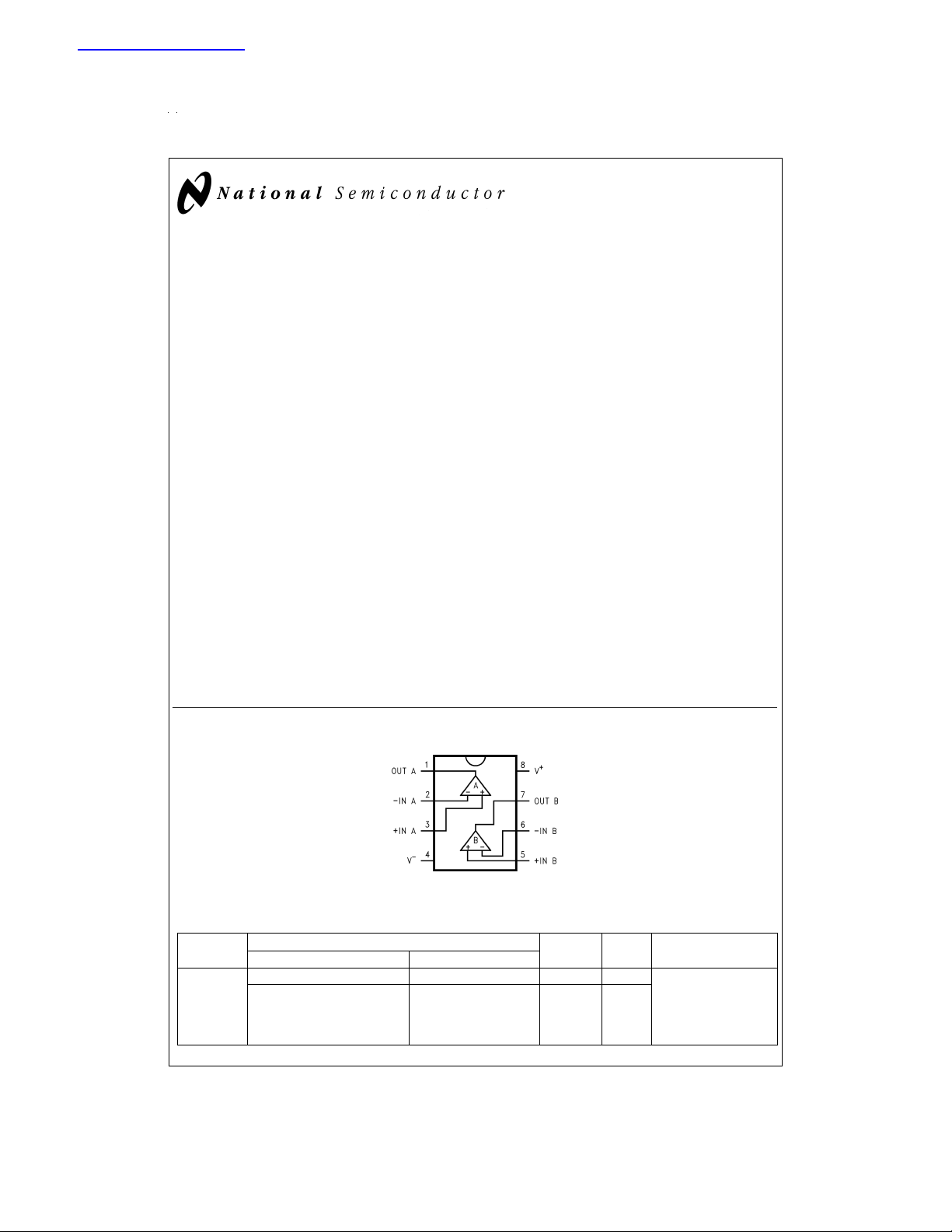
Connection Diagram
Key Specifications
Features
(Typical, V
n Output Swing to within 30 mV of supply rail
n High voltage gain 103 dB
n Gain Bandwidth Product 9.5 KHz
n Guaranteed for: 2.2V, 5V, 10V
n Low Supply Current 0.95 µA/Amplifier
n Input Voltage Range −0.3V to V
n Power consumption 2.1 µW/Amplifier
n Stable for A
=
2.2V)
S
≥+2 or AV≤ −1
V
+
-0.9V
Applications
n Portable instruments
n Smoke/gas/CO/fire detectors
n Pagers/cell phones
n Instrumentation
n Thermostats
n Occupancy sensors
n Cameras
n Active badges
DS100064-40
Top View
Ordering Information
Package
8-pin SO-8 LMC6442AIM, LMC6442IM - M08A Rails
© 1999 National Semiconductor Corporation DS100064 www.national.com
Industrial −40˚C to +85˚C Military −55˚C to +125˚C
LMC6442AIMX, LMC6442IMX - M08A
Temperature Range
NSC
Drawing
Supplied
AS
2.5K
Tape
and
Reel
Package Marking
LMC6442AIM
LMC6442IM
Page 2
Ordering Information (Continued)
Package
MSOP LMC6442AIMM, LMC6442IMM - MUA08A Rails
8-pin DIP
8-pin CDIP
10-pin SO
Industrial −40˚C to +85˚C Military −55˚C to +125˚C
LMC6442AIMMX,
LMC6442IMMX
LMC6442AIN, LMC6442IN - N08E
Temperature Range
-
-
- MUA08A
5962-9761301QPA J08A Rails LMC6442AMJ-QML
5962-9761301QXA WG10A Trays LMC6442AMWG-Q
NSC
Drawing
Supplied
AS
3K Tape
and
Reel
Rails LMC6442AIN,
Package Marking
A08A
LMC6442IN
5962-976130IQPA
9761301QXA
www.national.com 2
Page 3
Absolute Maximum Ratings (Note 1)
If Military/Aerospace specified devices are required,
please contact the National Semiconductor Sales Office/
Distributors for availability and specifications.
ESD Tolerance (Note 2) 2 kV
Differential Input Voltage
Voltage at Input/Output Pin (V
Supply Voltage (V
+−V−
): 16V
Current at Input Pin (Note 10)
Current at Output Pin(Notes 3, 7)
±
Supply Voltages
+
) + 0.3V, (V−) − 0.3V
±
5mA
±
30 mA
Lead Temp. (soldering 10 sec) 260˚C
Storage Temp. Range: −65˚C to +150˚C
Junction Temp. (Note 4) 150˚C
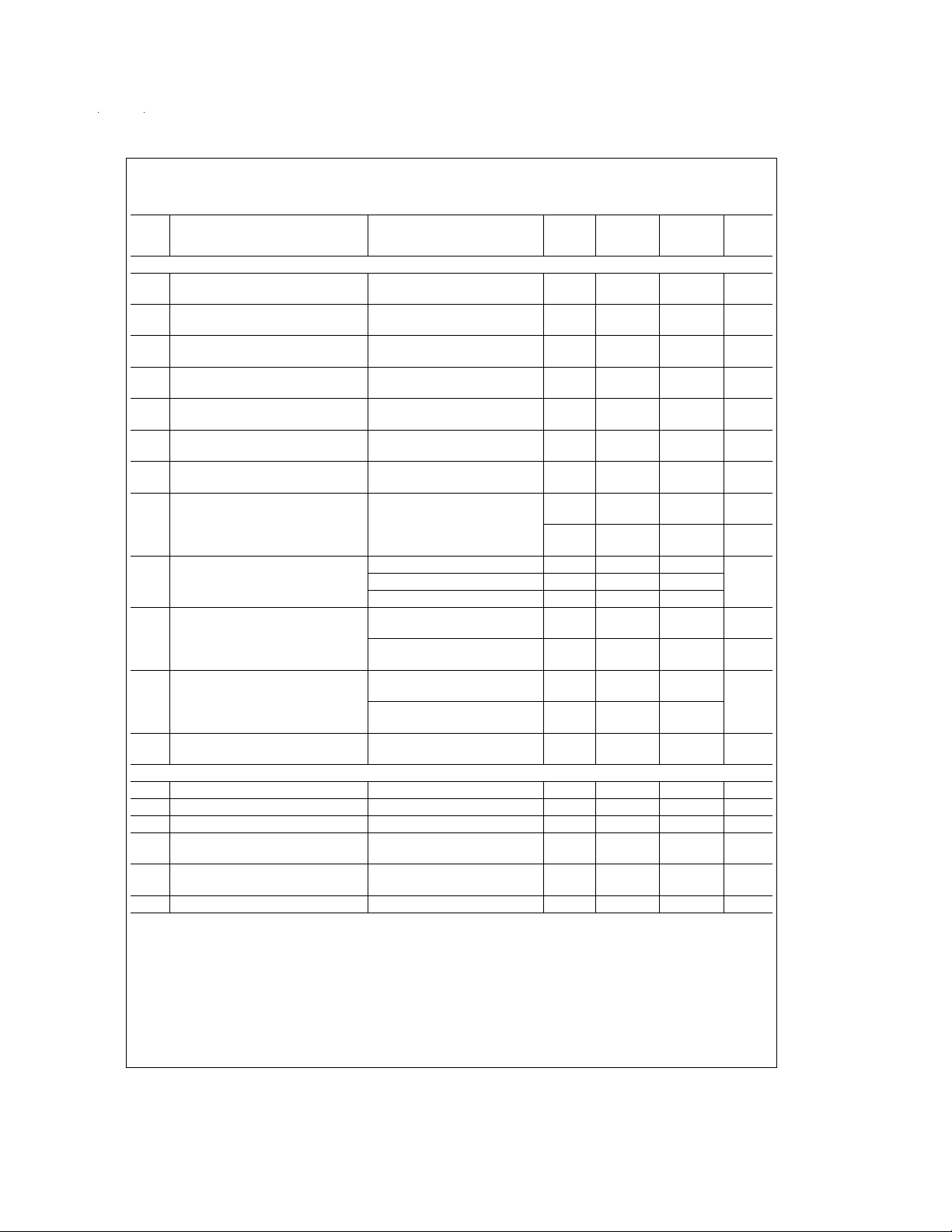
2.2V Electrical Characteristics
Unless otherwise specified, all limits guaranteed for T
Boldface limits apply at the temperature extremes.
Symbol Parameter Conditions
DC Electrical Characteristics
V
OS
TCV
I
B
I
OS
Input Offset Voltage
Temp. coefficient of input
OS
offset voltage
Input Bias Current (Note 14)
Input Offset Current (Note 14)
CMRR Common Mode Rejection
Ratio
C
IN
Common Mode Input
Capacitance
PSRR Power Supply Rejection Ratio V
V
CM
A
V
V
O
I
SC
I
S
Input Common-Mode Voltage
Range
Large Signal Voltage Gain Sourcing (Note 11) 100
Output Swing V
Output Short Circuit Current Sourcing, V
Supply Current (2 amplifiers) R
AC Electrical Characteristics
SR Slew Rate (Note 8) 2.2 V/ms
=
25˚C, V
J
−0.1V ≤ V
=
2.5 V to 10V
S
CM
CMRR ≥ 50 dB
Sinking(Note 11) 94
=
0.22V to 2V 103 80 80
V
O
=
100 mV (Note 13)
ID
=
−100 mV (Note 13) 22 60
V
ID
(Notes 12, 13)
Sinking, V
(Notes 12, 13)
V
ID
=
open 1.90 2.4
L
+
=
1.8V, R
Operating Ratings(Note 1)
Supply Voltage 1.8V ≤ V
Junction Temperature −40˚C
Range: LMC6442AI, LMC6442I
Thermal Resistance (θ
M Package, 8-pin Surface
Mount
MSOP Package 235˚C/W
N Package, 8-pin Molded
DIP
+
=
2.2V, V
−
=
0V, V
≤0.5V 92 67
=
100 mV
ID
=
−100 mV
=
open 2.10
L
)
JA
=
=
V
CM
Typ
(Note 5)
V
O
LMC6442AI
Limit
(Note 6)
−0.75
0.4 µV/˚C
0.005 44
0.0025 22
4.7 pF
95
1.3
−0.3 −0.2
2.18
50 18
50 20
+
/2, and R
±
3
±
4
67
75
75
1.05
0.95
0
2.15
2.15
60
17
19
3.0
<
T
J
=
1MΩto V
L
LMC6442I
Limit
(Note 6)
±
7
±
8
67
67
75
75
1.05
0.95
−0.2
0
2.15
2.15
60
60
18
17
20
19
2.6
3.2
≤ 11V
S
<
+85˚C
193˚C/W
115˚C/W
dB min
Units
max
max
max
max
max
max
+
mV
pA
pA
dB
min
V
min
V
dB
min
V
min
mV
µA
min
µA
/2.
www.national.com3
Page 4
2.2V Electrical Characteristics (Continued)
Unless otherwise specified, all limits guaranteed for T
Boldface limits apply at the temperature extremes.
=
J
25˚C, V
+
=
Symbol Parameter Conditions
AC Electrical Characteristics
GBWP Gain-Bandwidth Product 9.5 KHz
Phase Margin (Note 15) 63 Degree
φ
m
2.2V, V
−
=
0V, V
=
CM
Typ
(Note 5)
=
V
V
O
LMC6442AI
Limit
(Note 6)
+
/2, and R
=
1MΩto V
L
LMC6442I
Limit
(Note 6)
Units
+
/2.
5V Electrical Characteristics
Unless otherwise specified, all limits guaranteed for T
Boldface limits apply at the temperature extremes.
Symbol Parameter Conditions
=
J
25˚C, V
+
=
5V, V
−
=
0V, V
=
CM
Typ
(Note 5)
=
V
O
LMC6442AI
+
/2, and R
V
Limit
(Note 6)
=
1MΩto V
L
LMC6442I
Limit
(Note 6)
+
Units
DC Electrical Characteristics
V
OS
TCV
I
B
I
OS
Input Offset Voltage
Temp. coefficient of input
OS
offset voltage
Input Bias Current (Note 14)
Input Offset Current (Note 14)
CMRR Common Mode Rejection
Ratio
C
IN
Common Mode Input
Capacitance
PSRR Power Supply Rejection Ratio V
V
CM
A
V
Input Common-Mode Voltage
Range
Large Signal Voltage Gain Sourcing (Note 11) 100
−0.1V ≤ V
=
2.5 V to 10V
S
−0.75
0.4 µV/˚C
0.005 44
0.0025 22
≤3.5V 102 70
CM
4.1 pF
95
4.1
CMRR ≥ 50 dB
−0.4 −0.2
±
±
70
75
75
3.85
3.75
0
3
4
±
±
70
70
75
75
3.85
3.75
−0.2
0
7
8
dB min
Sinking (Note 11) 94
=
0.5V to 4.5V 103 80 80
V
O
V
O
I
SC
I
S
Output Swing V
Output Short Circuit Current Sourcing, V
Supply Current (2 amplifiers) R
=
100 mV
ID
(Note 13)
=
−100 mV
V
ID
(Note 13)
=
100 mV
(Notes 12, 13)
Sinking, V
(Notes 12, 13)
L
ID
=
−100 mV
ID
=
open 1.90 2.4
4.99 4.95
20 50
500 300
350 200
4.95
50
200
150
3.0
4.95
4.95
50
50
300
200
200
150
2.6
3.2
AC Electrical Characteristics
SR Slew Rate (Note 8) 4.1 2.5 2.5 V/ms
GBWP Gain-Bandwidth Product 10 KHz
φ
m
THD Total Harmonic Distortion A
Phase Margin (Note 15) 64 Degree
=
+2, f=100 Hz,
V
=
10MΩ,V
R
L
OUT
=
1 Vpp
0.08
/2.
mV
max
pA
max
pA
max
dB
min
V
min
V
max
dB
min
V
min
mV
max
µA
min
µA
max
%
www.national.com 4
Page 5
10V Electrical Characteristics
Unless otherwise specified, all limits guaranteed for T
Boldface limits apply at the temperature extremes.
Symbol Parameter Conditions
=
J
25˚C, V
+
=
10V, V
−
=
0V, V
=
CM
Typ
(Note 5)
=
V
V
O
LMC6442AI
Limit
(Note 6)
+
/2, and R
=
1MΩto V
L
LMC6442I
Limit
(Note 6)
Units
DC Electrical Characteristics
V
OS
TCV
I
B
I
OS
Input Offset Voltage
Temp. coefficient of input
OS
offset voltage
Input Bias Current (Note 14)
Input Offset Current (Note 14)
CMRR Common Mode Rejection
Ratio
C
IN
Common Mode Input
Capacitance
PSRR Power Supply Rejection Ratio V
V
CM
A
V
Input Common-Mode Voltage
Range
Large Signal Voltage Gain Sourcing (Note 11) 120
−0.1V ≤ V
=
2.5 V to 10V
S
−1.5
0.4 µV/˚C
0.005 44
0.0025 22
≤8.5V 105 70
CM
3.5 pF
95
9.1
CMRR ≥ 50 dB
−0.4 −0.2
±
±
70
75
75
8.85
8.75
0
3
4
±
±
70
70
75
75
8.85
8.75
−0.2
7
8
dB min
0
Sinking (Note 11) 100
=
0.5V to 9.5V 104 80 80
V
O
V
O
I
SC
I
S
Output Swing V
Output Short Circuit Current Sourcing, V
Supply Current (2 amplifiers) R
=
100 mV
ID
(Note 13)
=
V
−100 mV(Note 13) 22 50
ID
=
100 mV
(Notes 12, 13)
Sinking, V
(Notes 12, 13)
L
ID
=
−100 mV
ID
=
open 1.90 2.4
9.99 9.97
2100 1200
900 600
9.97
50
1000
500
3.0
9.97
9.97
50
50
1200
1000
600
500
2.6
3.2
AC Electrical Characteristics
SR Slew Rate(Note 8) 4.1 2.5 2.5 V/ms
GBWP Gain-Bandwidth Product 10.5 KHz
φ
m
e
n
i
n
Phase Margin (Note 15) 68 Degree
Input-Referred Voltage Noise R
Input-Referred Current Noise R
=
open
L
f=10 Hz
=
open
L
f=10 Hz
170 nV/
0.0002 pA/
Crosstalk Rejection (Note 9) 85 dB
+
/2.
mV
max
pA
max
pA
max
dB
min
V
min
V
max
dB
min
V
min
mV
max
µA
min
µA
max
√
Hz
√
Hz
www.national.com5
Page 6

Electrical Characteristics (continued)
Note 1: Absolute Maximum Ratings indicate limits beyond which damage to the device may occur. Operating Ratings indicate conditions for which the device is
intended to be functional, but specific performance is not guaranteed. For guaranteed specifications and the test conditions, see the Electrical Characteristics.
Note 2: Human body model, 1.5 kΩ in series with 100 pF.
Note 3: Applies to both single-supply and split-supply operation. Continuous short circuit operation at elevated ambient temperature can result in exceeding the
maximum allowed junction temperature of 150˚C. Output currents in excess of
Note 4: The maximumpowerdissipation is a function of T
-TA)/ θJA. All numbers apply for packages soldered directly into a PC board.
(max)
Note 5: Typical Values represent the most likely parametric norm.
Note 6: All limits are guaranteed by testing or statistical analysis unless otherwise specified.
Note 7: Do not short circuit output to V
Note 8: Slew rate is the slower of the rising and falling slew rates.
Note 9: Input referred, V
Note 10: Limiting input pin current is only necessary for input voltages that exceed absolute maximum input voltage ratings.
Note 11: R
L
Note 12: Output shorted to ground for sourcing, and shorted to V+ for sinking short circuit current test.
Note 13: V
ID
Note 14: Limits guaranteed by design.
Note 15: See the Typical Performance Characteristics and Application Notes sections for more details.
+
=
connected to V+/2. For Sourcing Test, V
is differential input voltage referenced to inverting input.
+
,when V+is greater than 13V or reliability will be adversely affected.
10V and R
=
10 MΩ connected to 5V. Each amp excited in turn with 1 KHz to produce about 10 Vpp output.
L
, θJA, and TA. The maximum allowable power dissipation at any ambient temperature is PD=(T
J(max)
>
V+/2. For Sinking tests, V
O
±
30 mA over long term may adversely affect reliability.
<
V+/2.
O
-
J
Typical Performance Characteristics V
Total Supply Current
vs Supply Voltage
DS100064-8
Input Bias Current
vs Temperature
Total Supply Current
vs Supply Voltage
(Negative Input Overdrive)
Offset Voltage vs
Common Mode Voltage
=
(V
2.2V)
S
=
5V, Single Supply, T
S
DS100064-9
=
25˚C unless otherwise specified
A
Total Supply Current
vs Supply Voltage
(Positive Input Overdrive)
Offset Voltage vs
Common Mode Voltage
=
(V
5V)
S
DS100064-10
DS100064-41
www.national.com 6
DS100064-6
DS100064-7
Page 7

Typical Performance Characteristics V
specified (Continued)
=
5V, Single Supply, T
S
=
25˚C unless otherwise
A
Offset Voltage vs
Common Mode Voltage
=
(V
10V)
S
Swing From Rail(s)
vs Temperature
DS100064-42
Swing Towards V−vs
Supply Voltage
Output Source Current
vs Output Voltage
DS100064-3
DS100064-49
Swing Towards V+vs
Supply Voltage
DS100064-2
Output Sink Current
vs Output Voltage
DS100064-48
Maximum Output Voltage
vs Load Resistance
DS100064-24
DS100064-1
Large Signal Voltage
Gain vs Supply Voltage
Open Loop
Gain/Phase vs
Frequency
DS100064-52
DS100064-19
www.national.com7
Page 8

Typical Performance Characteristics V
specified (Continued)
=
5V, Single Supply, T
S
=
25˚C unless otherwise
A
Open Loop
Gain/Phase vs
Frequency For Various C
=
(Z
L
1MΩII C
)
L
Phase Margin
(Worst Case)
vs Supply Voltage
L
DS100064-26
DS100064-23
Open Loop
Gain/Phase vs
Frequency For Various C
=
(Z
L
100 KΩ II C
)
L
CMRR vs Frequency
L
DS100064-25
DS100064-34
Gain Bandwidth Product
vs Supply Voltage
DS100064-21
PSRR vs Frequency
DS100064-15
Positive Slew Rate vs
Supply Voltage
DS100064-12
www.national.com 8
Negative Slew Rate vs
Supply Voltage
DS100064-11
Cross-Talk Rejection
vs Frequency
DS100064-18
Page 9

Typical Performance Characteristics V
specified (Continued)
=
5V, Single Supply, T
S
=
25˚C unless otherwise
A
Input Voltage Noise
vs Frequency
THD+N vs Amplitude
Large Signal Step
Response
=
+2) (C
=
100 pF)
L
(A
V
DS100064-16
DS100064-27
Output Impedance
vs Frequency
Maximum Output
Swing vs Frequency
Small Signal Step
Response
(A
pF)
=
V
−1)(C
=
1MΩ II 100 pF, 200
L
DS100064-33
DS100064-53
THD+N vs Frequency
Small Signal Step
Response
=
+2) (C
=
12 pF, 100 pF)
L
(A
V
Small Signal Step
Response
=
(A
+ 1) For Various C
V
DS100064-28
DS100064-29
L
DS100064-30
DS100064-51
DS100064-31
www.national.com9
Page 10

Typical Performance Characteristics V
specified (Continued)
Large Signal Step
Response
=
(A
V
+1) (C
=
L
200pF)
DS100064-32
Application Notes
Using LMC6442 in unity gain applications: LMC6442 is
optimized for maximum bandwidth and minimal external
components when operating at a minimum closed loop gain
of +2 (or −1). However, it is also possible to operate the device in a unity gain configuration by adding external compensation as shown in Figure 1:
DS100064-35
FIGURE 1. A
Using this compensation technique it is possible to drive capacitive loads of up to 300 pF without causing oscillations
(see the Typical Performance Characteristics for step response plots). This compensation can also be used with
other gain settings in order to improve stability, especially
when driving capacitive loads (for optimum performance, R
and Ccmay need to be adjusted).
Using “T” Network:
Compromises need to be made whenever high gain inverting stages need to achieve a high input impedance as well.
This is especially important in low current applications which
tend to deal with high resistance values. Using a traditional
inverting amplifier, gain is inversely proportional to the resistor value tied between the inverting terminal and input while
the input impedance is equal to this value. For example, in
order to build an inverting amplifier with an input impedance
of 10MΩ and a gain of 100, one needs to come up with a
feedback resistor of 1000MΩ -an expensive task.
An alternate solution is to use a “T” Network in the feedback
path, as shown in Fig. 2.
Closed loop gain, A
=
+1 Operation by adding C
V
is given by:
V
and R
c
c
c
=
5V, Single Supply, T
S
=
25˚C unless otherwise
A
DS100064-36
FIGURE 2. “T” Network Used to Replace High Value
Resistor
It must be noted, however, that using this scheme, the realizable bandwidth would be less than the theoretical maximum. With feedback factor, β, defined as:
BW(−3 dB)≈GBWP
β
•
In this case, assuming a GBWP of about 10 KHz, the expected BW would be around 50 Hz (vs 100 Hz with the conventional inverting amplifier).
Looking at the problem from a different view, with R
by A
Rin, one could select a value for R in the “T” Network
•
V
and then determine R1 based on this selection:
defined
F
www.national.com 10
DS100064-22
FIGURE 3. “T” Network Values for Various Values of R
Page 11

Application Notes (Continued)
For convenience, Fig. 3 shows R1 vs R
of R.
Design Considerations for Capacitive Loads: As with
many other opamps, the LMC6442 is more stable at higher
closed loop gains when driving a capacitive load. Figure 4
shows minimum closed loop gain versus load capacitance,
to achieve less than 10%overshoot in the output small signal response. In addition, the LMC6442 is more stable when
it provides more output current to the load and when its output voltage does not swing close to V
The LMC6442 is more tolerant to capacitive loads when the
equivalent output load resistance is lowered or when output
voltage is 1V or greater from the V
load drive capability is also improved by adding an isolating
resistor in series with the load and the output of the device.
Figure 5 shows the value of this resistor for various capacitive loads (A
%
overshoot.
=
−1), while limiting the output to less than 10
V
for different values
F
−
.
−
supply. The capacitive
FIGURE 4. Minimum Operating Gain vs Capactive Load
Referring to the Typical Performance Characteristics plot of
Phase Margin (Worst Case) vs Supply Voltage, note that
Phase Margin increases as the equivalent output load resistance is lowered. This plot shows the expected Phase Margin when the device output is very close to V
−
, which is the
least stable condition of operation. Comparing this Phase
Margin value to the one read off the Open Loop Gain/Phase
vs Frequency plot, one can predict the improvement in
Phase Margin if the output does not swing close to V
−
. This
dependence of Phase Margin on output voltage is minimized
as long as the output load, R
, is about 1MΩ or less.
L
Output Phase Reversal: The LMC6442 is immune against
this behavior even when the input voltages exceed the common mode voltage range.
Output Time Delay: Due to the ultra low power consumption of the device, there could be as long as 2.5 ms of time
delay from when power is applied to when the device output
reaches its final value.
DS100064-47
DS100064-43
FIGURE 5. Isolating Resistor Value vs Capactive Load
www.national.com11
Page 12

Application Circuits
Micropower Single Supply Voltage to Frequency Converter
+
=
5V: I
<
S
V
10µA, f/V
=
C
4.3 (Hz/V)
DS100064-45
DS100064-46
www.national.com 12
Page 13

Application Circuits (Continued)
Gain Stage with Current Boosting
DS100064-54
Offset Nulling Schemes
DS100064-44
www.national.com13
Page 14

Physical Dimensions inches (millimeters) unless otherwise noted
8-Lead (0.150″ Wide) Molded Small Outline Package, JEDEC
Order Number LMC6442AIM or LMC6442IM or LMC6442AIMX or LMC6442IMX
NS Package Number M08A
Order Number LMC6442AIN or LMC6442IN or LMC6442AINX or LMC6442INX
www.national.com 14
8-Lead (0.300″ Wide) Molded Dual-In-Line Package
NS Package Number N08E
Page 15

Physical Dimensions inches (millimeters) unless otherwise noted (Continued)
LMC6442 Dual Micropower Rail-to-Rail Output Single Supply Operational Amplifier
Order Number LMC6442AIMM or LMC6442IMM or LMC6442AIMMX or LMC6442IMMX
8-Lead (0.118″ Wide) Molded Mini Small Outline Package
NS Package Number MUA08A
LIFE SUPPORT POLICY
NATIONAL’S PRODUCTS ARE NOT AUTHORIZED FOR USE AS CRITICAL COMPONENTS IN LIFE SUPPORT
DEVICES OR SYSTEMS WITHOUT THE EXPRESS WRITTEN APPROVAL OF THE PRESIDENT OF NATIONAL
SEMICONDUCTOR CORPORATION. As used herein:
1. Life support devices or systems are devices or
systems which, (a) are intended for surgical implant
into the body, or (b) support or sustain life, and
whose failure to perform when properly used in
accordance with instructions for use provided in the
2. A critical component is any component of a life
support device or system whose failure to perform
can be reasonably expected to cause the failure of
the life support device or system, or to affect its
safety or effectiveness.
labeling, can be reasonably expected to result in a
significant injury to the user.
National Semiconductor
Corporation
Americas
Tel: 1-800-272-9959
Fax: 1-800-737-7018
Email: support@nsc.com
www.national.com
National does not assume any responsibility for use of any circuitry described, no circuit patent licenses are implied and National reserves the right at any time without notice to change said circuitry and specifications.
National Semiconductor
Europe
Fax: +49 (0) 1 80-530 85 86
Email: europe.support@nsc.com
Deutsch Tel: +49 (0) 1 80-530 85 85
English Tel: +49 (0) 1 80-532 78 32
Français Tel: +49 (0) 1 80-532 93 58
Italiano Tel: +49 (0) 1 80-534 16 80
National Semiconductor
Asia Pacific Customer
Response Group
Tel: 65-2544466
Fax: 65-2504466
Email: sea.support@nsc.com
National Semiconductor
Japan Ltd.
Tel: 81-3-5639-7560
Fax: 81-3-5639-7507
 Loading...