

查询LMC6061供应商
LMC6061
Precision CMOS Single Micropower Operational
Amplifier
General Description
The LMC6061 is a precision single low offset voltage, micropower operational amplifier, capable of precision single
supply operation. Performance characteristics include ultra
low input bias current, high voltage gain, rail-to-rail output
swing, and an input common mode voltage range that includes ground.These features, plus its low power consumption, make the LMC6061 ideally suited for battery powered
applications.
Other applications using the LMC6061 include precision
full-wave rectifiers, integrators, references, sample-and-hold
circuits, and true instrumentation amplifiers.
This device is built with National’s advanced double-Poly
Silicon-Gate CMOS process.
For designs that require higher speed, see the LMC6081
precision single operational amplifier.
For a dual or quad operational amplifier with similar features,
see the LMC6062 or LMC6064 respectively.
PATENT PENDING
November 1994
n Low offset voltage: 100 µV
n Ultra low supply current: 20 µA
n Operates from 4.5V to 15V single supply
n Ultra low input bias current: 10 fA
n Output swing within 10 mV of supply rail, 100k load
n Input common-mode range includes V
n High voltage gain: 140 dB
n Improved latchup immunity
−
Applications
n Instrumentation amplifier
n Photodiode and infrared detector preamplifier
n Transducer amplifiers
n Hand-held analytic instruments
n Medical instrumentation
n D/A converter
n Charge amplifier for piezoelectric transducers
LMC6061 Precision CMOS Single Micropower Operational Amplifier
Features
(Typical Unless Otherwise Noted)
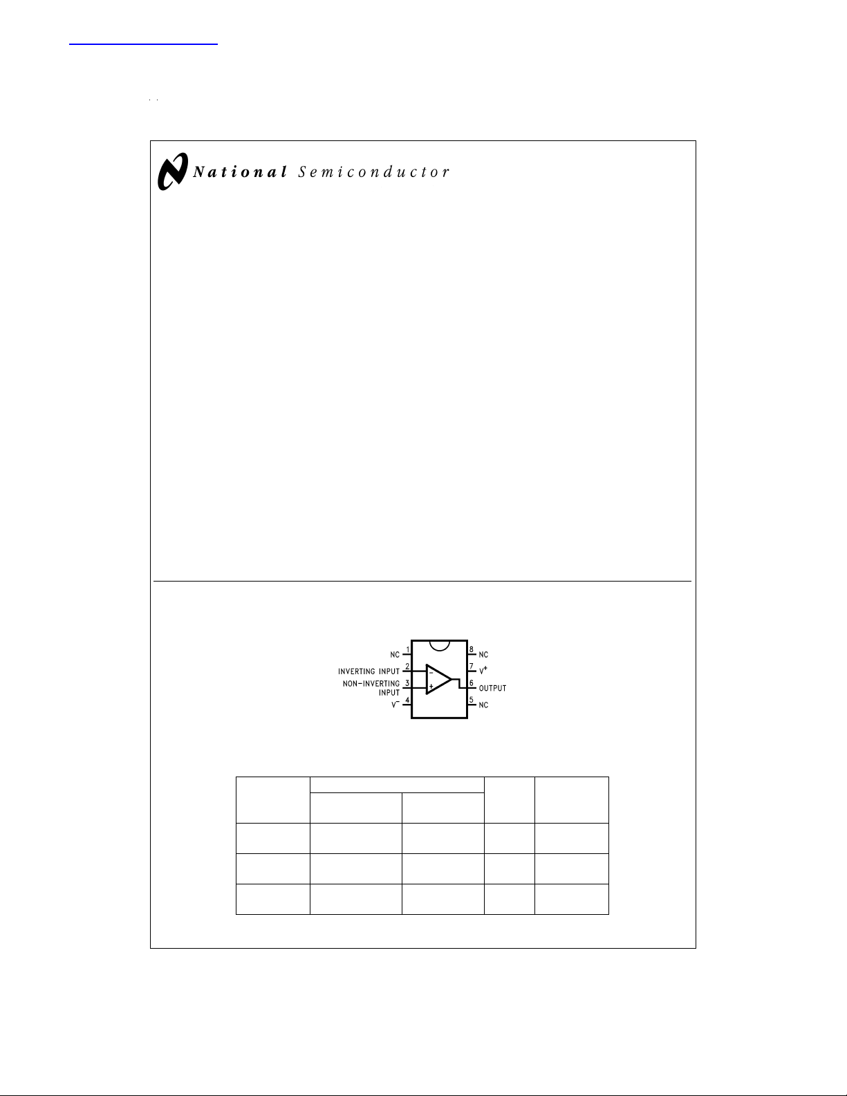
Connection Diagram
Ordering Information
Package Temperature Range NSC
8-Pin LMC6061AMN LMC6061AIN N08E Rail
Molded DIP LMC6061IN
8-Pin LMC6061AIM M08A Rail
Small Outline LMC6061IM Tape and Reel
8-Pin LMC6061AMJ/883 J08A Rail
Ceramic DIP
8-Pin DIP/SO
Top View
Military Industrial
−55˚C to +125˚C −40˚C to +85˚C
DS011422-1
Drawing
Transport
Media
© 1999 National Semiconductor Corporation DS011422 www.national.com
Absolute Maximum Ratings (Note 1)
If Military/Aerospace specified devices are required,
please contact the National Semiconductor Sales Office/
Distributors for availability and specifications.
Differential Input Voltage
Voltage at Input/Output Pin (V
+−V−
Supply Voltage (V
Output Short Circuit to V
Output Short Circuit to V
) 16V
+
−
Lead Temperature 260˚C
(Soldering, 10 sec.)
Storage Temp. Range −65˚C to +150˚C
Junction Temperature 150˚C
ESD Tolerance (Note 4) 2 kV
±
Supply Voltage
+
) +0.3V,
−
) −0.3V
(V
(Note 10)
(Note 2)
±
Current at Input Pin
Current at Output Pin
10 mA
±
30 mA
Current at Power Supply Pin 40 mA
Power Dissipation (Note 3)
Operating Ratings (Note 1)
Temperature Range
LMC6061AM −55˚C ≤ T
LMC6061AI, LMC6082I −40˚C ≤ T
Supply Voltage 4.5V ≤ V
Thermal Resistance (θ
) (Note 11)
JA
N Package, 8-Pin Molded DIP 115˚C/W
M Package, 8-Pin Surface Mount 193˚C/W
Power Dissipation (Note 9)
≤ +125˚C
J
≤ +85˚C
J
+
≤ 15.5V
DC Electrical Characteristics
Unless otherwise specified, all limits guaranteed for T
=
0V, V
=
1.5V, V
CM
=
2.5V and R
O
>
1M unless otherwise specified.
L
=
25˚C. Boldface limits apply at the temperature extremes. V
J
+
=
5V, V
Typ LMC6061AM LMC6061AI LMC6061I
Symbol Parameter Conditions (Note 9) Limit Limit Limit Units
(Note 6) (Note 6) (Note 6)
V
Input Offset Voltage 100 350 350 800 µV
OS
1200 900 1300 Max
TCV
Input Offset Voltage 1.0 µV/˚C
OS
Average Drift
I
B
Input Bias Current 0.010 pA
100 4 4 Max
I
OS
Input Offset Current 0.005 pA
100 2 2 Max
R
IN
Input Resistance
CMRR Common Mode 0V ≤ V
+
Rejection Ratio V
=
+PSRR Positive Power Supply 5V ≤ V
Rejection Ratio V
=
O
−PSRR Negative Power Supply 0V ≤ V
≤ 12.0V 85 75 75 66 dB
CM
15V 70 72 63 Min
+
≤ 15V 85 75 75 66 dB
2.5V 70 72 63 Min
−
≤ −10V 100 84 84 74 dB
>
10 Tera Ω
Rejection Ratio 70 81 71 Min
+
V
Input Common-Mode V
CM
=
5V and 15V −0.4 −0.1 −0.1 −0.1 V
Voltage Range for CMRR ≥ 60 dB 000Max
+
V
− 1.9 V+− 2.3 V+− 2.3 V+− 2.3 V
A
Large Signal R
V
=
100 kΩ Sourcing 4000 400 400 300 V/mV
L
+
V
− 2.6 V+− 2.5 V+− 2.5 Min
Voltage Gain (Note 7) 200 300 200 Min
Sinking 3000 180 180 90 V/mV
70 100 60 Min
=
R
25 kΩ Sourcing 3000 400 400 200 V/mV
L
(Note 7) 150 150 80 Min
Sinking 2000 100 100 70 V/mV
35 50 35 Min
−
www.national.com 2
DC Electrical Characteristics (Continued)
Unless otherwise specified, all limits guaranteed for T
=
0V, V
=
1.5V, V
CM
=
2.5V and R
O
>
1M unless otherwise specified.
L
=
25˚C. Boldface limits apply at the temperature extremes. V
J
Typ LMC6061AM LMC6061AI LMC6061I
Symbol Parameter Conditions (Note 9) Limit Limit Limit Units
(Note 6) (Note 6) (Note 6)
+
V
Output Swing V
O
=
5V 4.995 4.990 4.990 4.950 V
=
R
100 kΩ to 2.5V 4.970 4.980 4.925 Min
L
0.005 0.010 0.010 0.050 V
0.030 0.020 0.075 Max
+
=
V
5V 4.990 4.975 4.975 4.950 V
=
R
25 kΩ to 2.5V 4.955 4.965 4.850 Min
L
0.010 0.020 0.020 0.050 V
0.045 0.035 0.150 Max
+
=
V
15V 14.990 14.975 14.975 14.950 V
=
R
100 kΩ to 7.5V 14.955 14.965 14.925 Min
L
0.010 0.025 0.025 0.050 V
0.050 0.035 0.075 Max
+
=
V
15V 14.965 14.900 14.900 14.850 V
=
R
25 kΩ to 7.5V 14.800 14.850 14.800 Min
L
0.025 0.050 0.050 0.100 V
0.200 0.150 0.200 Max
I
O
Output Current Sourcing, V
+
=
V
5V 8108Min
Sinking, V
=
0V 22 16 16 13 mA
O
=
5V 21 16 16 16 mA
O
788Min
I
O
Output Current Sourcing, V
+
=
V
15V 91010Min
Sinking, V
=
0V 25 15 15 15 mA
O
=
13V 35 24 24 24 mA
O
(Note 10) 788Min
+
I
S
Supply Current V
=
+5V, V
=
1.5V 20 24 24 32 µA
O
35 32 40 Max
+
V
=
+15V, V
=
7.5V 24 30 30 40 µA
O
40 38 48 Max
+
=
5V, V
−
AC Electrical Characteristics
Unless otherwise specified, all limits guaranteed for T
−
=
V
Symbol Parameter Conditions (Note 5) Limit Limit Limit Units
SR Slew Rate (Note 8) 35 20 20 15 V/ms
GBW Gain-Bandwidth Product 100 kHz
θ
m
e
n
i
n
T.H.D. Total Harmonic Distortion F=1 kHz, A
=
0V, V
1.5V, V
CM
Phase Margin 50 Deg
Input-Referred Voltage Noise F=1 kHz 83
Input-Referred Current Noise F=1 kHz 0.0002
=
O
2.5V and R
>
1M unless otherwise specified.
L
=
100 kΩ,V
R
L
±
5V Supply
=
25˚C, Boldface limits apply at the temperature extremes. V
J
Typ LMC6061AM LMC6061AI LMC6061I
(Note 6) (Note 6) (Note 6)
8107Min
=
−5
V
=
2V
O
PP
0.01
+
=
5V,
%
www.national.com3
AC Electrical Characteristics (Continued)
Note 1: Absolute Maximum Ratings indicate limits beyond which damage to the device may occur. Operating Ratings indicate conditions for which the device is in-
tended to be functional, but do not guarantee specific performance limits. For guaranteed specifications and test conditions, see the Electrical Characteristics. The
guaranteed specifications apply only for the test conditions listed.
Note 2: Applies to both single-supply and split-supply operation. Continous shortcircuitoperationatelevatedambienttemperaturecan result in exceeding the maximum allowed junction temperature of 150˚C. Output currents in excess of
Note 3: The maximum power dissipation is a function of T
−TA)/θJA.
Note 4: Human body model, 1.5 kΩ in series with 100 pF.
Note 5: Typical values represent the most likely parametric norm.
Note 6: All limits are guaranteed by testing or statistical analysis.
+
Note 7: V
Note 8: V
Note 9: For operating at elevated temperatures the device must be derated based on the thermal resistance θ
Note 10: Do not connect output to V
Note 11: All numbers apply for packages soldered directly into a PC board.
Note 12: For guaranteed Military Temperature Range parameters see RETSMC6061X.
=
+
=
=
15V, V
15V. Connected as Voltage Follower with 10V step input. Number specified is the slower of the positive and negative slew rates.
CM
7.5V and R
connected to 7.5V. For Sourcing tests, 7.5V ≤ VO≤ 11.5V. For Sinking tests, 2.5V ≤ VO≤ 7.5V.
L
+
, when V+is greater than 13V or reliability witll be adversely affected.
J(Max)
±
, θJA, and TA. The maximum allowable power dissipation at any ambient temperature is P
30 mA over long term may adversely affect reliability.
=
with P
JA
(T
D
J–TA
)/θJA.
=
(T
D
J(Max)
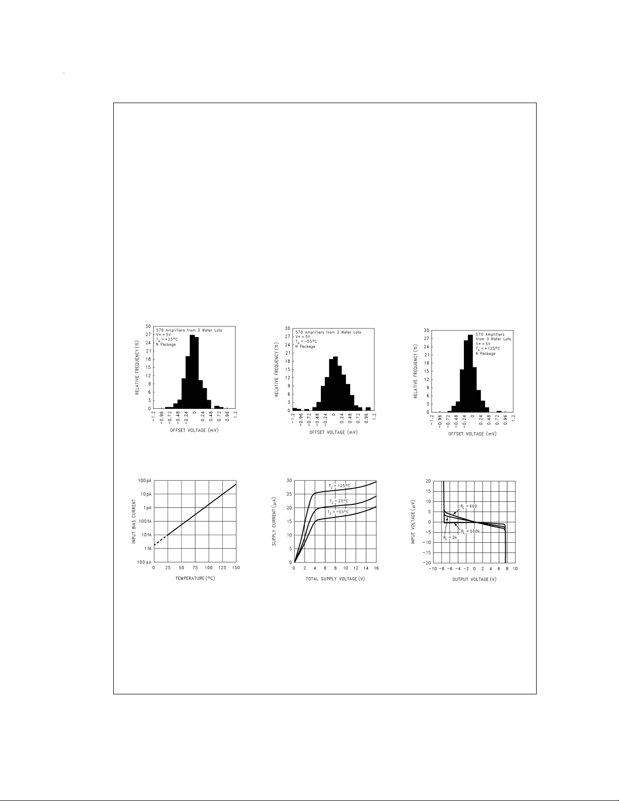
Typical Performance Characteristics V
Distribution of LMC6061
Input Offset Voltage
=
(T
+25˚C)
A
Input Bias Current
vs Temperature
DS011422-15
Distribution of LMC6061
Input Offset Voltage
=
(T
−55˚C)
A
Supply Current
vs Supply Voltage
=
±
S
7.5V, T
=
25˚C, Unless otherwise specified
A
Distribution of LMC6061
Input Offset Voltage
=
(T
+125˚C)
A
DS011422-16
DS011422-17
Input Voltage
vs Output Voltage
DS011422-18
www.national.com 4
DS011422-19
DS011422-20
 Loading...