

查询LM6041IN供应商
LMC6041
CMOS Single Micropower Operational Amplifier
LMC6041 CMOS Single Micropower Operational Amplifier
December 1994
General Description
Ultra-low power consumption and low input-leakage current
are the hallmarks of the LMC6041. Providing input currents
of only 2 fA typical, the LMC6041 can operate from a single
supply, has output swing extending to each supply rail, and
an input voltage range that includes ground.
The LMC6041 is ideal for use in systems requiring ultra-low
power consumption. In addition, the insensitivity to latch-up,
high output drive, and output swing to ground without requiring external pull-down resistors make it ideal for
single-supply battery-powered systems.
Other applications for the LMC6041 include bar code reader
amplifiers, magnetic and electric field detectors, and
hand-held electrometers.
This device is built with National’s advanced Double-Poly
Silicon-Gate CMOS process.
See the LMC6042 for a dual, and the LMC6044 for a quad
amplifier with these features.
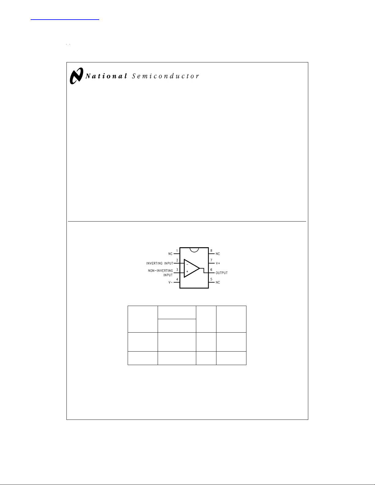
Connection Diagram
8-Pin DIP/SO
Ordering Information
Temperature
Range
−40˚C to +85˚C
8-Pin LMC6041AIM M08A Rail
Small Outline LMC6041IM Tape and
8-Pin LMC6041AIN N08E Rail
Molded DIP LM6041IN
Features
n Low supply current: 14 µA (Typ)
n Operates from 4.5V to 15.5V single supply
n Ultra low input current: 2 fA (Typ)
n Rail-to-rail output swing
n Input common-mode range includes ground
Applications
n Battery monitoring and power conditioning
n Photodiode and infrared detector preamplifier
n Silicon based transducer systems
n Hand-held analytic instruments
n pH probe buffer amplifier
n Fire and smoke detection systems
n Charge amplifier for piezoelectric transducers
DS011136-1
NSC
Drawing
Transport
MediaPackage Industrial
Reel
© 1999 National Semiconductor Corporation DS011136 www.national.com
Absolute Maximum Ratings (Note 1)
If Military/Aerospace specified devices are required,
please contact the National Semiconductor Sales Office/
Distributors for availability and specifications.
Differential Input Voltage
Supply Voltage (V
Output Short Circuit to V
Output Short Circuit to V
+−V−
) 16V
−
+
Lead Temperature
(Soldering, 10 sec.) 260˚C
Storage Temperature Range −65˚C to +150˚C
Junction Temperature 110˚C
ESD Tolerance (Note 4) 500V
Current at Input Pin
±
Supply Voltage
(Note 2)
(Note 11)
±
5mA
Current at Output Pin
Current at Power Supply Pin 35 mA
Voltage at Input/Output Pin (V
+
) + 0.3V, (V−) − 0.3V
±
18 mA
Power Dissipation (Note 3)
Operating Ratings
Temperature Range
LMC6041AI, LMC6041I −40˚C ≤ T
Supply Voltage 4.5V ≤ V
Power Dissipation (Note 9)
Thermal Resistance (θ
) (Note 10)
JA
8-Pin DIP 101˚C/W
8-Pin SO 165˚C/W
≤ +85˚C
J
+
≤ 15.5V
Electrical Characteristics
Unless otherwise specified, all limits guaranteed for T
5V, V
−
=
0V, V
=
1.5V, V
CM
+
=
/2, and R
V
O
>
1M unless otherwise specified.
L
=
=
T
25˚C. Boldface limits apply at the temperature extremes. V
A
J
+
=
Typical LMC6041AI LMC6041I Units
Symbol Parameter Conditions (Note 5) Limit Limit (Limit)
(Note 6) (Note 6)
V
Input Offset Voltage 1 3 6 mV
OS
3.3 6.3 max
TCV
Input Offset Voltage 1.3 µV/˚C
OS
Average Drift
I
B
Input Bias Current 0.002 44pA
max
I
OS
Input Offset Current 0.001 22pA
max
R
IN
Input Resistance
CMRR Common Mode 0V ≤ V
+
Rejection Ratio V
=
+PSRR Positive Power Supply 5V ≤ V
Rejection Ratio V
=
O
−PSRR Negative Power Supply 0V ≤ V
Rejection Ratio V
CMR Input Common-Mode V
=
O
+
=
≤ 12.0V 75 68 62 dB
CM
15V 66 60 min
+
≤ 15V 75 68 62 dB
2.5V 66 60 min
−
≤ −10V 94 84 74 dB
2.5V 83 73 min
5V and 15V −0.4 −0.1 −0.1 V
>
10 TeraΩ
Voltage Range for CMRR ≥ 50 dB 00max
+
V
− 1.9V V+− 2.3V V+− 2.3V V
A
Large Signal R
V
=
100 kΩ (Note 7) Sourcing 1000 400 300 V/mV
L
+
V
− 2.5V V+− 2.4V min
Voltage Gain 300 200 min
Sinking 500 180 90 V/mV
120 70 min
=
R
25 kΩ (Note 7) Sourcing 1000 200 100 V/mV
L
160 80 min
Sinking 250 100 50 V/mV
60 40 min
www.national.com 2
Electrical Characteristics (Continued)
=
Unless otherwise specified, all limits guaranteed for T
5V, V
−
=
0V, V
=
1.5V, V
CM
+
=
/2, and R
V
O
>
1M unless otherwise specified.
L
=
T
25˚C. Boldface limits apply at the temperature extremes. V
A
J
Typical LMC6041AI LMC6041I Units
Symbol Parameter Conditions (Note 5) Limit Limit (Limit)
(Note 6) (Note 6)
+
V
Output Swing V
O
=
5V 4.987 4.970 4.940 V
=
R
100 kΩ to V
L
+
/2 4.950 4.910 min
0.004 0.030 0.060 V
0.050 0.090 max
+
=
V
5V 4.980 4.920 4.870 V
=
R
25 kΩ to V
L
+
/2 4.870 4.820 min
0.010 0.080 0.130 V
0.130 0.180 max
+
=
V
15V 14.970 14.920 14.880 V
=
R
100 kΩ to V
L
+
/2 14.880 14.820 min
0.007 0.030 0.060 V
0.050 0.090 max
+
=
V
15V 14.950 14.900 14.850 V
=
R
25 kΩ to V
L
+
/2 14.850 14.800 min
0.022 0.100 0.150 V
0.150 0.200 max
I
SC
Output Current Sourcing, V
+
=
V
5V 10 8 min
Sinking, V
=
0V 22 16 13 mA
O
=
5V 21 16 13 mA
O
88min
I
SC
Output Current Sourcing, V
+
=
V
15V 10 10 min
Sinking, V
=
0V 40 15 15 mA
O
=
13V 39 24 21 mA
O
(Note 11) 88min
I
S
Supply Current V
=
1.5V 14 20 26 µA
O
24 30 max
+
=
V
15V 18 26 34 µA
31 39 max
+
=
AC Electrical Characteristics
Unless otherwise specified, all limits guaranteed for T
5V, V
−
=
0V, V
=
1.5V, V
CM
O
=
+
/2, and R
V
>
1M unless otherwise specified.
L
=
=
T
25˚C. Boldface limits apply at the temperature extremes. V
A
J
+
Typ LMC6041AI LMC6041I Units
Symbol Parameter Conditions (Note 5) Limit Limit (Limit)
(Note 6) (Note 6)
SR Slew Rate (Note 8) 0.02 0.015 0.010 V/µs
0.010 0.007 min
GBW Gain-Bandwidth Product 75 kHz
φ
m
e
n
Phase Margin 60 Deg
Input-Referred F=1 kHz 83 nV/√Hz
Voltage Noise
i
n
Input-Referred F=1 kHz 0.0002 pA/√Hz
Current Noise
T.H.D. Total Harmonic F=1 kHz, A
Distortion R
=
L
±
5V Supply
V
100 kΩ,V
=
−5
=
2V
O
pp
0.01
%
www.national.com3
=
AC Electrical Characteristics (Continued)
Note 1: Absolute Maximum Ratings indicate limits beyond which damage to the device may occur. Operating conditions indicate conditions for which the device is
intended to be functional, but do not guarantee specific performance limits. For guaranteed specifications and test conditions, see the Electrical Characteristics. The
guaranteed specifications apply only for the test conditions listed.
Note 2: Applies to both single-supply and split-supply operation. Continuous short circuit operation at elevated ambient temperature can result in exceeding the
maximum allowed junction temperature of 110˚C. Output currents in excess of
Note 3: The maximum powerdissipationisa function of T
−TA)/θJA.
Note 4: Human body model, 1.5 kΩ in series with 100 pF.
Note 5: Typical Values represent the most likely parametric norm.
Note 6: All limits are guaranteed at room temperature (standard type face) or at operating temperature extremes (bold face type).
+
=
Note 7: V
+
=
Note 8: V
Note 9: For operating at elevated temperatures the device must be derated based on the thermal resistance θ
Note 10: All numbers apply for packages soldered directly into a PC board.
Note 11: Do not connect output to V
=
15V, V
15V. Connected as Voltage Follower with 10V step input. Number specified in the slower of the positive and negative slew rates.
CM
7.5V and R
connected to 7.5V. For Sourcing tests, 7.5V ≤ VO≤ 11.5V. For Sinking tests, 2.5V ≤ VO≤ 7.5V.
L
+
when V+is greater than 13V or reliability may be adversely affected.
, θJA, and TA. The maximum allowable power dissipation at any ambient temperature is P
J(max)
±
30 mA over long term may adversely affect reliability.
=
with P
JA
(T
D
J−TA
)/θJA.
=
(T
D
J(max)
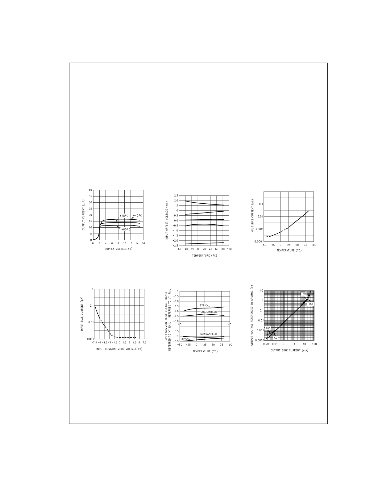
Typical Performance Characteristics V
Supply Current vs
Supply Voltage
DS011136-19
Input Bias Current
vs Input Common-Mode
Voltage
Offset Voltage vs
Temperature of Five
Representative Units
Input Common-Mode
Voltage Range vs
Temperature
=
±
S
7.5V, T
=
25˚C unless otherwise specified
A
Input Bias Current
vs Temperature
DS011136-20
DS011136-21
Output Characteristics
Current Sinking
DS011136-22
www.national.com 4
DS011136-23
DS011136-24
 Loading...