

查询LMC6022供应商
LMC6022
Low Power CMOS Dual Operational Amplifier
General Description
The LMC6022 is a CMOS dual operational amplifier which
can operate from either a single supply or dual supplies. Its
performance features include an input common-mode range
that reachesV
100k and 5 kΩ loads) that is equal to or better than widely
accepted bipolar equivalents, while the power supply requirement is less than 0.5 mW.
This chip is built with National’s advanced Double-Poly
Silicon-Gate CMOS process.
See the LMC6024 datasheet for a CMOS quad operational
amplifier with these same features.
Features
n Specified for 100 kΩ and5kΩloads
n High voltage gain: 120 dB
n Low offset voltage drift: 2.5 µV/˚C
−
, lowinputbiascurrent, and voltage gain (into
n Ultra low input bias current: 40 fA
n Input common-mode range includes V
n Operating range from +5V to +15V supply
n Low distortion: 0.01%at 1 kHz
n Slew rate: 0.11 V/µs
n Micropower operation: 0.5 mW
−
Applications
n High-impedance buffer or preamplifier
n Current-to-voltage converter
n Long-term integrator
n Sample-and-hold circuit
n Peak detector
n Medical instrumentation
n Industrial controls
LMC6022 Low Power CMOS Dual Operational Amplifier
November 1994
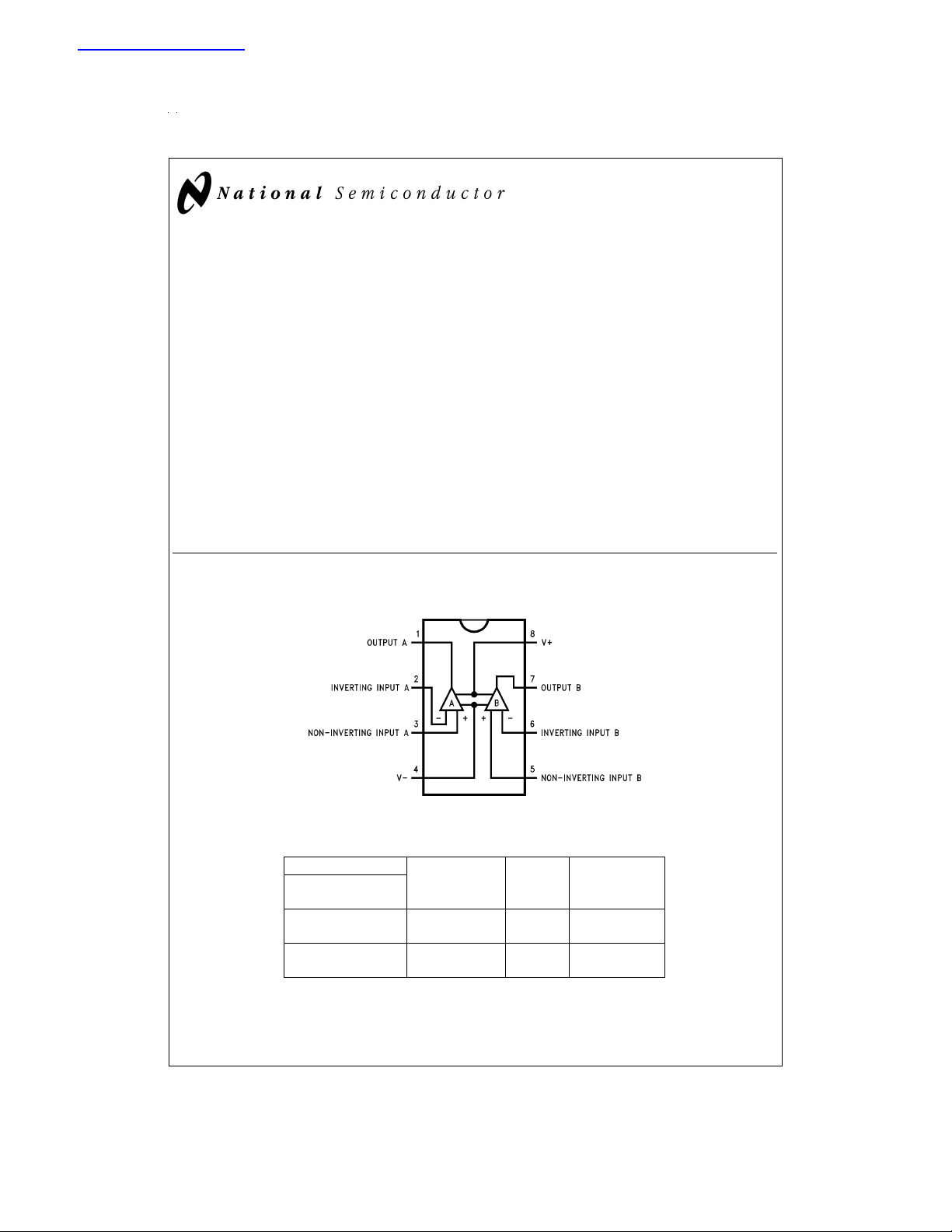
Connection Diagram
Ordering Information
Temperature Range
Industrial
−40˚C ≤ T
LMC6022IN 8-Pin N08E Rail
LMC6022IM 8-Pin M08A Rail
≤ +85˚C
J
8-Pin DIP/SO
DS011236-1
Top View
Package
Molded DIP
Small Outline Tape and Reel
NSC
Drawing
Transport
Media
© 1999 National Semiconductor Corporation DS011236 www.national.com
Absolute Maximum Ratings (Note 1)
±
Differential Input Voltage
Supply Voltage (V
+−V−
) 16V
Lead Temperature
(Soldering, 10 sec.) 260˚C
Storage Temperature Range −65˚C to +150˚C
Junction Temperature 150˚C
ESD Tolerance (Note 4) 1000V
Voltage at Output/Input Pin (V
Current at Output Pin
Current at Power Supply Pin 35 mA
Power Dissipation (Note 3)
Supply Voltage
+
) +0.3V, (V−) −0.3V
±
18 mA
Current at Input Pin
Output Short Circuit to V
Output Short Circuit to V
−
+
±
5mA
(Note 2)
(Note 12)
Operating Ratings
Temperature Range −40˚C ≤ TJ≤ +85˚C
Supply Voltage Range 4.75V to 15.5V
Power Dissipation (Note 10)
Thermal Resistance (θ
8-Pin DIP 101˚C/W
8-Pin SO 165˚C/W
), (Note 11)
JA
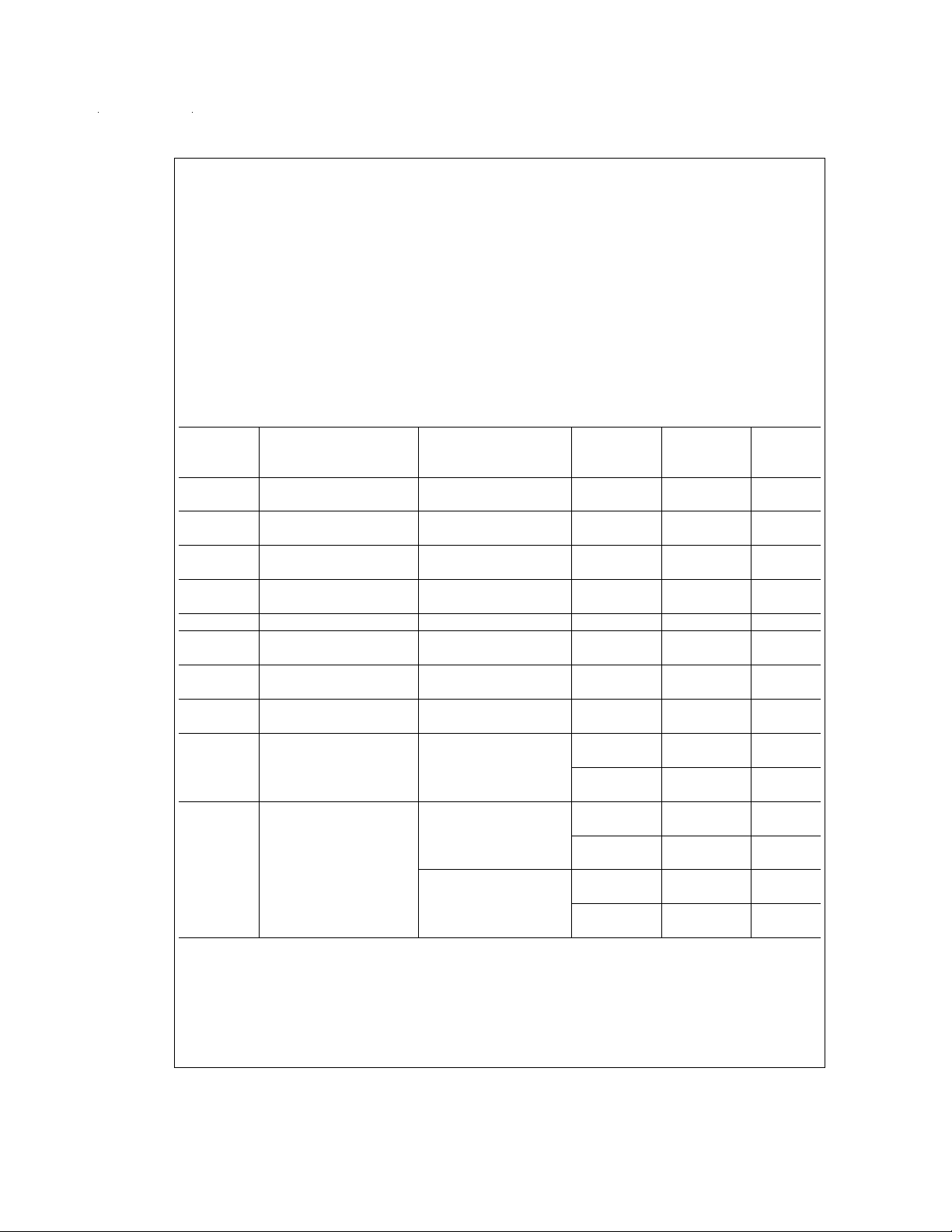
DC Electrical Characteristics
The following specifications apply for V
face limits apply at the temperature extremes; all other limits T
Symbol Parameter Conditions
V
OS
Input Offset Voltage 1 9 mV
+
−
=
5V, V
=
0V, V
=
1.5V, V
CM
J
=
25˚C.
=
2.5V, and R
O
=
1M unless otherwise noted. Bold-
L
Typical
(Note 5)
LMC6022I
(Note 6)
11 max
∆V
/∆T Input Offset Voltage 2.5 µV/˚C
OS
Average Drift
I
B
Input Bias Current 0.04 pA
200 max
I
OS
Input Offset Current 0.01 pA
100 max
R
IN
Input Resistance
CMRR Common Mode 0V ≤ V
+
Rejection Ratio V
=
+PSRR Positive Power Supply 5V ≤ V
≤ 12V 83 63 dB
CM
15V 61 min
+
≤ 15V 83 63 dB
>
1 TeraΩ
Rejection Ratio 61 min
−PSRR Negative Power Supply 0V ≤ V
−
≤ −10V 94 74 dB
Rejection Ratio 73 min
+
V
CM
Input Common-Mode V
=
5V & 15V −0.4 −0.1 V
Voltage Range For CMRR ≥ 50 dB 0 max
+
V
− 1.9 V+− 2.3 V
A
V
Large Signal R
=
100 kΩ (Note 7) 1000 200 V/mV
L
+
V
− 2.5 min
Voltage Gain Sourcing 100 min
Sinking 500 90 V/mV
40 min
=
R
5kΩ(Note 7) 1000 100 V/mV
L
Sourcing 75 min
Sinking 250 50 V/mV
20 min
UnitsLimit
www.national.com 2
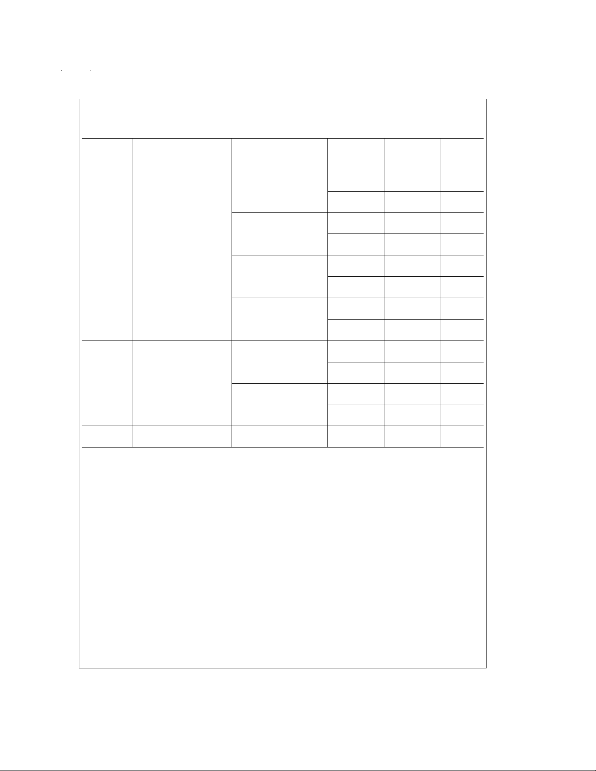
DC Electrical Characteristics (Continued)
The following specifications apply for V
face limits apply at the temperature extremes; all other limits T
+
Symbol Parameter Conditions
V
O
I
O
I
S
Output Voltage Swing V
Output Current V
Supply Current Both Amplifiers 86 140 µA
−
=
5V, V
=
0V, V
CM
+
=
5V 4.987 4.40 V
=
R
100 kΩ to 2.5V 4.43 min
L
+
=
V
5V 4.940 4.20 V
=
R
5kΩto 2.5V 4.00 min
L
+
=
V
15V 14.970 14.00 V
=
R
100 kΩ to 7.5V 13.90 min
L
+
=
V
15V 14.840 13.70 V
=
R
5kΩto 7.5V 13.50 min
L
+
=
5V 22 13 mA
Sourcing, V
Sinking, V
O
O
(Note 2) 9 min
+
=
V
15V 40 23 mA
Sourcing, V
Sinking, V
O
O
(Note 12) 15 min
=
V
1.5V 165 max
O
=
1.5V, V
J
=
25˚C.
=
2.5V, and R
O
=
1M unless otherwise noted. Bold-
L
Typical
(Note 5)
LMC6022I
(Note 6)
0.004 0.06 V
0.09 max
0.040 0.25 V
0.35 max
0.007 0.06 V
0.09 max
0.110 0.32 V
0.40 max
=
0V 9 min
=
5V 21 13 mA
=
0V 15 min
=
13V 39 23 mA
UnitsLimit
www.national.com3
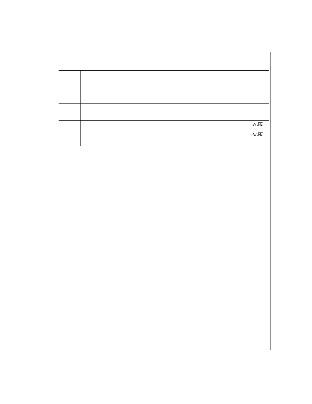
AC Electrical Characteristics
The following specifications apply for V
Boldface limits apply at the temperature extremes; all other limits T
Symbol Parameter Conditions
+
−
=
5V, V
=
0V, V
=
1.5V, V
CM
J
=
O
25˚C.
=
2.5V, and R
Typical
(Note 5)
=
1M unless other otherwise noted.
L
LMC6022I
(Note 6)
UnitsLimit
SR Slew Rate (Note 8) 0.11 0.05 V/µs
0.03 min
GBW Gain-Bandwidth Product 0.35 MHz
φ
M
G
M
Phase Margin 50 Deg
Gain Margin 17 dB
Amp-to-Amp Isolation (Note 9) 130 dB
e
n
Input-Referred Voltage Noise F=1 kHz 42
i
n
Note 1: Absolute Maximum Ratings indicate limits beyond which damage to component may occur. Operating Ratings indicate conditions for which the device is intended to be functional, but do not guarantee specific performance limits. For guaranteed specifications and test conditions, see the Electrical Characteristics. The
guaranteed specifications apply only for the test conditions listed.
Note 2: Applies to both single-supply and split-supply operation. Continuous short circuit operation at elevated ambient temperature and/or multiple Op Amp shorts
can result in exceeding the maximum allowed junction temperature of 150˚C. Output currents in excess of
Note 3: The maximum power dissipation is a function of T
−TA)/θJA.
Note 4: Human body model, 100 pF discharged through a 1.5 kΩ resistor.
Note 5: Typical values represent the most likely parametric norm.
Note 6: All limits are guaranteed by testing or correlation.
Note 7: V
Note 8: V
Note 9: Input referred. V
Note 10: For operating at elevated temperatures the device must be derated based on the thermal resistance θ
Note 11: All numbers apply for packages soldered directly into a PC board.
Note 12: Do not connect output to V
Input-Referred Current Noise F=1 kHz 0.0002
±
, θJAand TA. The maximum allowable power dissipation at any ambient temperature is P
J(max)
+
=
+
=
=
15V, V
15V. Connected as Voltage Follower with 10V step input. Number specified is the slower of the positive and negative slew rates.
CM
7.5V, and R
+
=
connected to 7.5V. For Sourcing tests, 7.5V ≤ VO≤ 11.5V. For Sinking tests, 2.5V ≤ VO≤ 7.5V.
L
15V and R
=
100 kΩ connected to 7.5V. Each amp excited in turn with 1 kHz to produce V
L
+
when V+is greater than 13V or reliability may be adversely affected.
30 mA over long term may adversely affect reliability.
=
13 V
O
PP
=
with P
JA
(T
D
J−TA
.
)/θJA.
=
(T
D
J(max)
www.national.com 4
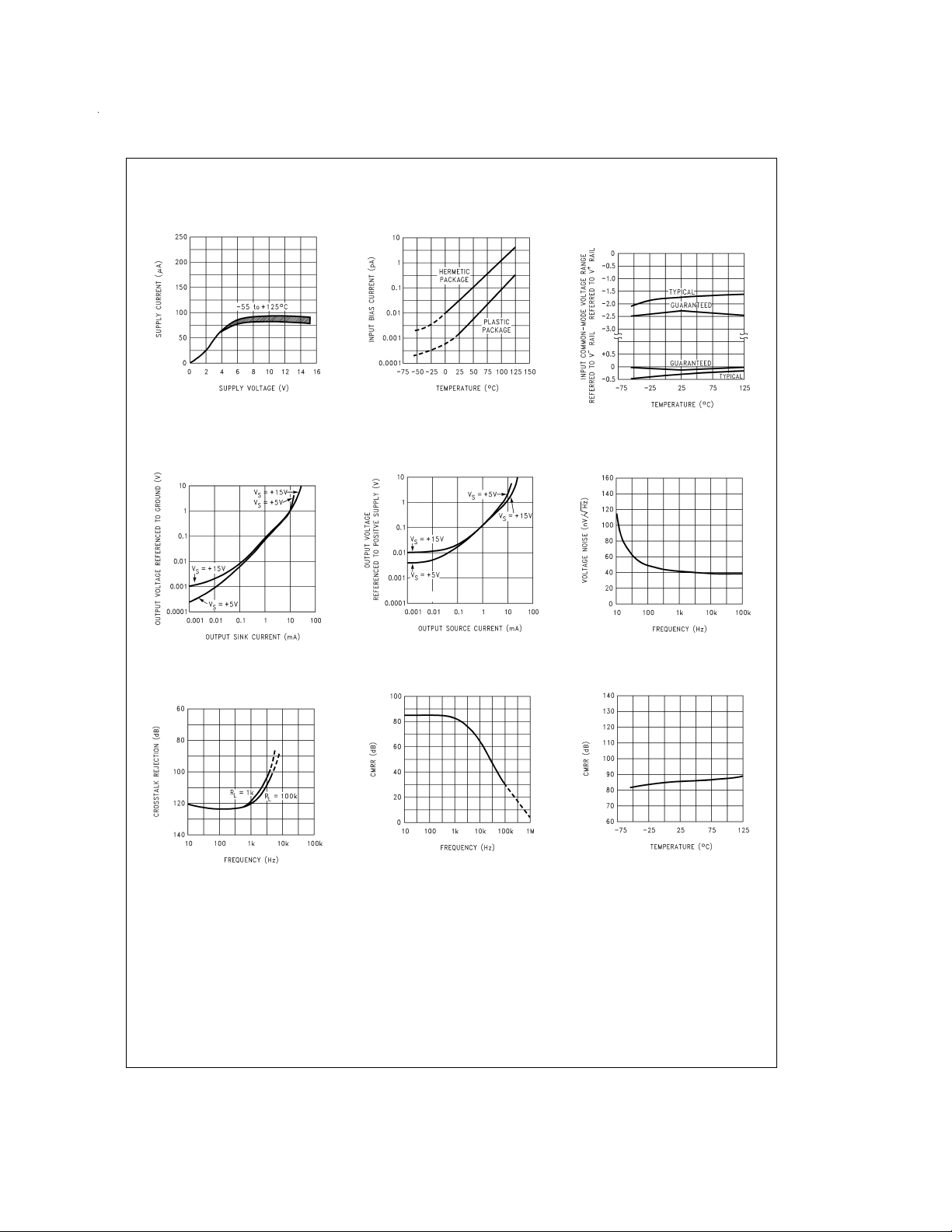
Typical Performance Characteristics V
Supply Current
vs Supply Voltage
Input Bias Current
vs Temperature
=
±
S
7.5V, T
=
25˚C unless otherwise specified
A
Input Common-Mode
Voltage Range vs
Temperature
Output Characteristics
Current Sinking
Crosstalk Rejection
vs Frequency
DS011236-27
DS011236-30
Output Characteristics
Current Sourcing
CMRR vs Frequency
DS011236-28
DS011236-31
DS011236-29
Input Voltage Noise
vs Frequency
DS011236-32
CMRR vs Temperature
DS011236-33
DS011236-34
DS011236-35
www.national.com5
 Loading...