

Page 1
查询LMC6009供应商
LMC6009
9 Channel Buffer Amplifier for TFT-LCD
LMC6009 9 Channel Buffer Amplifier for TFT-LCD
May 1999
General Description
The LMC6009 is a CMOS integrated circuit that buffers 9 reference voltages for gamma correction in a Thin Film Transistor Liquid Crystal Display (TFT-LCD). Guaranteed to operate
at both 3.3V and 5V supplies, this integrated circuit contains
nine, independent unity gain buffers that can source 130 mA
into a capacitive load without oscillation.
The LMC6009 is useful for buffering gamma voltages into
column drivers that employ the resistor-divider architecture.
High output current capabilityandfastsettlingcharacteristics
of this device improve display quality by minimizing rise time
errors at the outputs of the column driver. The integration of
nine buffers and a multiplexer eliminates the need for discrete buffers and a separate multiplexer (MUX) chip on the
panel.
The LMC6009 is available in 48-pin surface mount TSSOP.
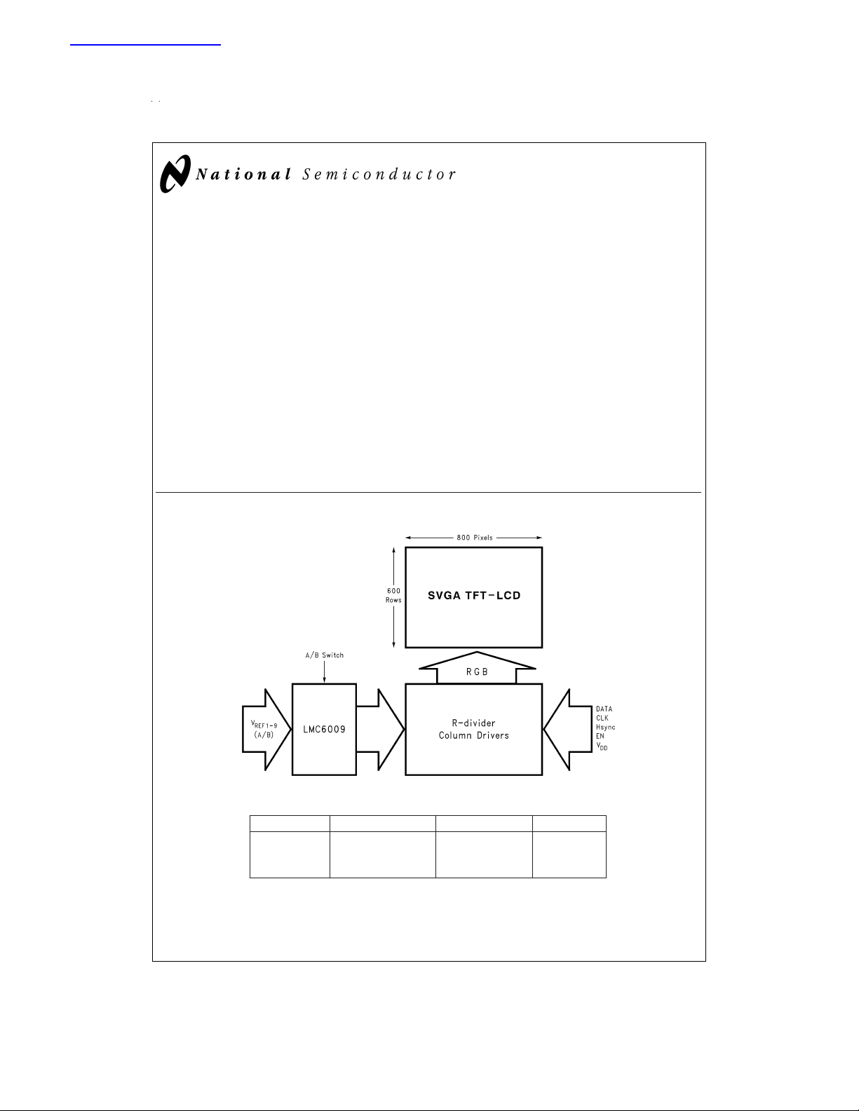
Application in VGA/SVGA TFT-LCD
Features
n Number of inputs 18
n 3.3V and 5V operation
n Supply current 3.5 mA
n Settling time 3 µs
n A/B channel inputs for asymmetrical Gamma
n Number of outputs 9
n Number of control inputs 1
n Built-in thermal shutdown protection
Applications
n VGA/SVGA TFT-LCD drive circuits
n Electronic Notebooks
n Electronic Games
n Personal Communication Devices
n Personal Digital Assistants (PDA)
DS012533-1
Ordering Information
Package Temperature Range Transport Media NSC Drawing
48-pin TSSOP −20˚C–+75˚C MTD48
LMC6009MT
LMC6009MTX Tape and Reel
© 1999 National Semiconductor Corporation DS012533 www.national.com
Page 2

Absolute Maximum Ratings (Note 1)
If Military/Aerospace specified devices are required,
please contact the National Semiconductor Sales Office/
Distributors for availability and specifications.
ESD Tolerance 1.0 kV
Input Voltage GND–0.3V ≤ V
Supply Voltage (VDD) −0.3 to +6.5 V
Operating Temperature −20˚C to +75˚C
Storage Temperature Range −55˚C to +150˚C
+
+0.3V
V
DD
Maximum Junction Temperature (T
Maximum Power Dissipation (P
) +150˚C
J
) 1.09W
D
Operating Ratings (Note 1)
Supply Voltage 2.7V ≤ V
≤
Frequency DC-50 kHz
DC
Thermal Resistance (θ
DC
Derating 8.70 mW/˚C
)
JA
DD
≤ 5.5V
3V DC Electrical Characteristics
Unless otherwise specified, all limits are guaranteed for T
=
25˚C, and V
J
Symbol Parameter Conditions Min Typ Max Units
V
DD
V
OS
I
B
V
OL
Supply Voltage 2.7 3.0 3.3 V
Offset Voltage RS= 10k 20 mV
Input Bias Current 1500 nA
Output Voltage, Low Amp A8 and A9
=13mA
I
SINK
Amp A1–A7
=13mA
I
V
OH
Output Voltage, High Amp A1 and A2
SINK
I
SOURCE
=13mA
Amp A3–A9
=13mA
I
I
SC
I
DD
∆V
V
IH
V
IL
I
IH
I
IL
A
V
Note 1: See Test Circuit (
Output Short Circuit Current V
Supply Current No Load 3.5 5 mA
Load Regulation VIN= 0.3–3 V
L
A/B Switch Logic Voltage, High Select A 2 V
A/B Switch Logic Voltage, Low Select B 0.8 V
A/B Switch Logic Current, High 1.5 µA
A/B Switch Logic Current, Low 1µA
Voltage Gain 0.985 V/V
Figure 2
)
SOURCE
- 1.65V (Note 1) 80 150 mA
OUT
I
SOURCE
I
SINK
DC
=13mA
= 13 mA +10 mV
=
DD
3.0 V
.
DC
GND +
0.2
GND +
0.6
V
–0.2 V
DD
V
–0.6 V
DD
−10 mV
5V DC Electrical Characteristics
Unless otherwise specified, all limits are guaranteed for T
=
25˚C, and V
J
Symbol Parameter Conditions Min Typ Max Units
V
DD
V
OS
I
B
V
OL
Supply Voltage 4.5 5 5.5 V
Offset Voltage RS= 10k 20 mV
Input Bias Current 1500 nA
Output Voltage, Low Amp A8 and A9
=20mA
I
SINK
Amp A1–A7
=20mA
I
V
OH
Output Voltage, High Amp A1 and A2
SINK
I
SOURCE
=20mA
Amp A3–A9
=20mA
I
I
SC
I
DD
Output Short Circuit Current V
Supply Current No Load 4.5 6 mA
SOURCE
- 1.65V (Note 1) 120 200 mA
OUT
=
.
5V
DD
DC
GND +
0.2
GND +
1.0
V
–0.2 V
DD
V
–1.0 V
DD
V
V
V
V
www.national.com 2
Page 3
5V DC Electrical Characteristics (Continued)
Unless otherwise specified, all limits are guaranteed for T
=
25˚C, and V
J
Symbol Parameter Conditions Min Typ Max Units
∆V
V
IH
V
IL
I
IH
I
IL
A
V
Load Regulation VIN= 0.5–4.5 V
L
I
SOURCE
I
= 20 mA +10 mV
SINK
=20mA
DC
A/B Switch Logic Voltage, High Select A 2 V
A/B Switch Logic Voltage, Low Select B 0.8 V
A/B Switch Logic Current, High 1.5 µA
A/B Switch Logic Current, Low 1µA
Voltage Gain 0.985 V/V
=
.
5V
DD
DC
−10 mV
AC Electrical Characteristics
Unless otherwise specified, all limits are guaranteed for T
=
25˚C, and V
J
Symbol Parameter Conditions Min Typ Max Units
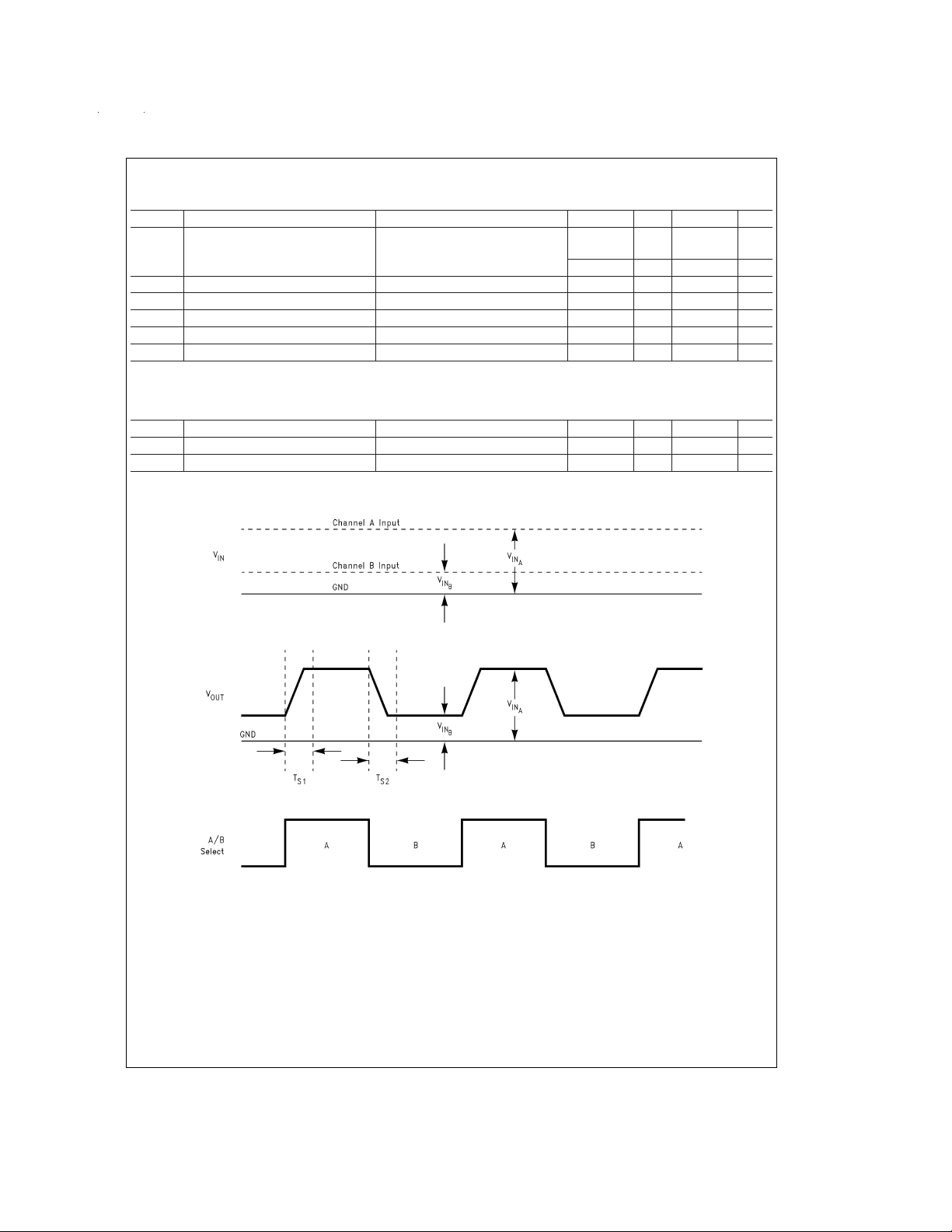
T
S1
T
S2
Note 2: See test circuits (
Settling Time 1 (Note 2) IDC= 13 mA (Sink/Source) 3 6 µs
Settling Time 2 (Note 2) IDC= 13 mA (Sink/Source) 3 6 µs
Figure 3,Figure 4
and
Figure 5
)
=
.
3V
DD
DC
FIGURE 1. Rise and Fall Times at Outputs
DS012533-2
www.national.com3
Page 4

AC Electrical Characteristics
(Continued)
FIGURE 2.
DS012533-3
DS012533-5
FIGURE 4. 13 mA Sink/Source
FIGURE 3. A1: 13 mA Source only
A2–A4: 13 mA Sink/Source
Description of Pins; LMC6009
Pin 1 NC Pin 25 NC
Pin 2 NC Pin 26 NC
Pin 3 NC Pin 27 NC
Pin 4 A1 in (A) Pin 28 NC
Pin 5 A1 in (B) Pin 29 A/B Switch
Pin 6 A2 in (A) Pin 30 V
Pin 7 A2 in (B) Pin 31 GND (C)
Pin 8 A3 in (A) Pin 32 A9 out
Pin 9 A3 in (B) Pin 33 A8 out
Pin 10 A4 in (A) Pin 34 A7 out
Pin 11 A4 in (B) Pin 35 A6 out
Pin 12 A5 in (A) Pin 36 A5 out
Pin 13 A5 in (B) Pin 37 GND (B)
Pin 14 A6 in (A) Pin 38 V
Pin 15 A6 in (B) Pin 39 A4 out
Pin 16 A7 in (A) Pin 40 A3 out
Pin 17 A7 in (B) Pin 41 A2 out
Pin 18 A8 in (A) Pin 42 A1 out
Pin 19 A8 in (B) Pin 43 GND (A)
Pin 20 A9 in (A) Pin 44 V
Pin 21 A9 in (B) Pin 45 NC
Pin 22 NC Pin 46 NC
Pin 23 NC Pin 47 NC
Pin 24 NC Pin 48 NC
DS012533-4
FIGURE 5. A6–A8: 13 mA Sink/Source
A9: 13 mA Sink Only
(C)
DD
(B)
DD
(A)
DD
DS012533-6
www.national.com 4
Page 5

Block Diagram
FIGURE 6. Block Diagram of LMC6009
Applications
The LMC6009 is useful for buffering the nine reference voltages for gamma correction in a TFT-LCD as shown in
Figure 7
. The A/B channel inputs allow the user to alternate
two sets of gamma references to compensateforasymmetrical Gamma characteristic during Row Inversion. The
LMC6009 eliminates the need for nine external switches or
an 18-to-9 multiplexer.
DS012533-8
Since the buffers in the LMC6009 draw extremely low bias
current (1.5 µA max), large resistance values can be used in
the reference voltage string. This allows the power dissipation in the gamma reference circuit to be minimized. The
nine buffers are guaranteed to deliver 80 mA to the load, allowing the pixel voltages of the TFT-LCD to settle very
quickly.
www.national.com5
Page 6

Applications (Continued)
FIGURE 7.
Example: Below is a calculation of pixel charge time (for a
black to black transition) in a VGAdisplay operating at a vertical refresh rate of 60 Hz, with a panel capacitance of 50 pF
per sub-pixel:
A full black to black transition represents the maximum
charging time for the panel, since it requires that the panel
capacitance be driven by a 4V swing from node V
(
Figure 7
).
REF1
Total capacitive load presented to the LMC6009 is
=
50pFx3x640=96 nF
C
L
Output current of the LMC6009 is:
=
80 mA
I
SC
Hence, slew time t
=
(96 nF x 4V)/80 mA=3.07 µs
SLEW
The total line time for a VGA system is approximately 34 µs.
Therefore, the LMC6009 easily meets the drive requirements for the application.The input resistance seen between
the V
www.national.com 6
REFn
and V
inputs, (where n=0 thru 8) of the
REF(n+1)
DS012533-7
Column Driver (
Figure 7
) also draw current from the
LMC6009. Thus, the actual current available for charging the
panel capacitance is:
Ipx=80 mA - (V
VREF1–VVREF2
)/R
CD
where
=
V
V
R
Voltage at node V
V REFn
VREF(n+1)
CD
=
Voltage at node V
=
Column driver input resistance between
REFn
,
REF(n+1)
, and
VREFn and VREF(n+1)
Since the LMC6009 is capable of sourcing 80 mA, the pixel
charging time is primarily limited only by the length of the
R
time constant. To implement a high quality display,
CD.CL
column drivers that allow the shortest possible time constant
(lower values of R
of R
result in increased system quiescent power dissipa-
CD
tion. It is therefore important to optimize systemperformance
) are desirable. However, lower values
CD
by carefully considering speed vs power tradeoffs.
Page 7

Physical Dimensions inches (millimeters) unless otherwise noted
All dimensions are in millimeters
48-Lead Molded Thin Shrink Small Outline Package, JEDEC
NS Package Number MTD48
LMC6009 9 Channel Buffer Amplifier for TFT-LCD
LIFE SUPPORT POLICY
NATIONAL’S PRODUCTS ARE NOT AUTHORIZED FOR USE AS CRITICAL COMPONENTS IN LIFE SUPPORT
DEVICES OR SYSTEMS WITHOUT THE EXPRESS WRITTEN APPROVAL OF THE PRESIDENT AND GENERAL
COUNSEL OF NATIONAL SEMICONDUCTOR CORPORATION. As used herein:
1. Life support devices or systems are devices or
systems which, (a) are intended for surgical implant
into the body, or (b) support or sustain life, and
whose failure to perform when properly used in
accordance with instructions for use provided in the
2. A critical component is any component of a life
support device or system whose failure to perform
can be reasonably expected to cause the failure of
the life support device or system, or to affect its
safety or effectiveness.
labeling, can be reasonably expected to result in a
significant injury to the user.
National Semiconductor
Corporation
Americas
Tel: 1-800-272-9959
Fax: 1-800-737-7018
Email: support@nsc.com
www.national.com
National does not assume any responsibility for use of any circuitry described, no circuit patent licenses are implied and National reserves the right at any time without notice to change said circuitry and specifications.
National Semiconductor
Europe
Fax: +49 (0) 1 80-530 85 86
Email: europe.support@nsc.com
Deutsch Tel: +49 (0) 1 80-530 85 85
English Tel: +49 (0) 1 80-532 78 32
Français Tel: +49 (0) 1 80-532 93 58
Italiano Tel: +49 (0) 1 80-534 16 80
National Semiconductor
Asia Pacific Customer
Response Group
Tel: 65-2544466
Fax: 65-2504466
Email: sea.support@nsc.com
National Semiconductor
Japan Ltd.
Tel: 81-3-5639-7560
Fax: 81-3-5639-7507
 Loading...