

查询LMC6008供应商
LMC6008
8 Channel Buffer
LMC6008 8 Channel Buffer
April 1996
General Description
The LMC6008 octal buffer is designed specifically to buffer
the multi-level voltages going to the inputs of the integrated
circuits. The LMC6008 AC characteristics, including settling
time, are specified for a capacitive load of 0.1 mF for this
reason.
The LMC6008 contains 4 high-speed buffers and 4 lowpower buffers. The high-speed buffers can provide an output current of at least 250 mA (minimum), and the low-power buffers can provide at least 150 mA (minimum). By including the 2 types of buffers, the LMC6008 is able to provide
this function while consuming a supply current of only 6.5
mA (maximum). The buffers are a rail-to-rail design, which
typically swing to within 30 mV of either supply.
The LMC6008 also contains a standby function which puts
the buffer into a high-impedance mode. The supply current
in the standby mode is a low 500 mA max. Also, a thermal
limit circuit is included to protect the device from overload
conditions.
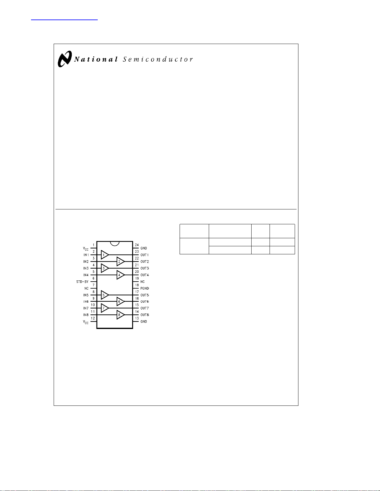
Connection Diagram
24-Pin SO
Features
Y
High Output Current:
High Speed Buffers 250 mA min
Low Power Buffers 150 mA min
Y
Slew Rate:
High Speed Buffers 1.7 V/ms
Low Power Buffers 0.85V/ms
Y
Settling Time, C
Y
Wide Input/Output Range 0.1V to V
Y
Supply Voltage Range 5V to 16V
Y
Supply Current 6.5 mA max
Y
Standby Mode Current 500 mA
e
0.1 mF16ms max
L
CC
b
0.1V min
Applications
Y
AMLCD voltage buffering
Y
Multi-voltage buffering
Ordering Information
Package
24-Pin LMC6008IM M24B Rail
Surface Mount
Temperature Range NSC Transport
b
40§Ctoa85§C Drawing Media
LMC6008IMX M24B Tape & Reel
Note: Buffers 1, 3, 5 and 7 are High Speed and
Buffers 2, 4, 6 and 8 are Low Speed.
C
1996 National Semiconductor Corporation RRD-B30M56/Printed in U. S. A.
Top View
TL/H/12321
TL/H/12321– 1
Absolute Maximum Ratings (Note 1)
If Military/Aerospace specified devices are required,
please contact the National Semiconductor Sales
Office/Distributors for availability and specifications.
ESD Tolerance (Note 2) 2000V
Voltage at Input Pin V
Voltage at Output Pin V
a
Supply Voltage (V
b
Vb) 16V
Lead Temperature
(soldering, 10 sec.) 260
Storage Temperature Range
Junction Temperature (Note 4) 150§C
Power Dissipation (Note 4) Internally Limited
a
a
0.4V, V
a
a
0.4V, V
b
55§Ctoa150§C
b
b
0.4V
b
b
0.4V
Operating Ratings (Note 1)
a
s
s
V
C/W
§
16V
Supply Voltage 4.5V
Temperature Range
b
20§Ctoa100§C
Thermal Resistance (iJA)
M Package, 24-Pin Surface Mount 50
C
§
DC Electrical Characteristics
Unless otherwise specified, all limits guaranteed for T
J
e
25§C, V
Symbol Parameter Conditions
V
OS
A
V
I
B
I
LP
I
LP
V
ERR
V
IH
V
IL
I
IH
I
IL
I
O (STD-BY)
I
CC
I
STD-BY
Input Offset Voltage R
e
V
10 V
O
PP
Input Bias Current 300 nA max
Peak Load Current Hi Speed Buffers
Peak Load Current Lo Speed Buffers
Output Voltage Difference
(Note 9)
Standby Logic
HIgh Voltage
I
Low Voltage
STANDBY
Logic
Standby High Input Current 1.0 mA max
Standby Low Input Current 1.0 mA max
Output Leakage Current V
Supply Current V
Standby Current V
PSRR Power Supply Rejection Ratio 5VkV
V
O
Voltage Output Swing 0.1 V min
e
10 kX 25 mV max
S
e
V
13 V
O
PP
e
V
13 V
O
PP
e
STD-BY
e
Low, V
IL
e
STD-BY
k
CC
CC
e
14.5V and R
e
0.
L
Typ
(Note 5)
LMC6008
Limit
(Note 6)
Units
0.985 V/V
b
250 mA max
a
250 mA min
b
150 mA max
a
150 mA min
35 mV max
3.30 V min
1.80 V max
High 5 mA max
e
7.25V 6.5 mA max
IN
High 500 mA max
14.5V 55 dB min
b
V
0.1 V max
CC
http://www.national.com 2
AC Electrical Characteristics
Unless otherwise specified, all limits guaranteed for T
Symbol Parameter Conditions
J
e
25§C, V
CC
e
14.5V and R
e
0X.
L
Typ
(Note 5)
LMC6008
Limit
(Note 6)
Units
SR Slew Rate Buffers 1, 3, 5, 7 (Note 3) 1.70 V/ms min
Buffers 2, 4, 6, 8 (Note 3) 0.85 V/ms min
t
S
t
ON
t
OFF
PBW Power Bandwidth V
C
L
Note 1: Absolute Maximum Ratings indicate limits beyond which damage to the device may occur. Operating ratings indicate conditions for which the device is
intended to be functional, but specific performance is not guaranteed. For guaranteed specifications and the test conditions, see the Electrical Characteristics.
Note 2: Human body model, 1.5 kX in series with 100 pF.
Note 3: The Load is a series connection of a 0.1 mF capacitor and a 1X resistor.
Note 4: The maximum power dissipation is a function of T
e
(T
P
D
limit circuit will limit the die temperature to approximately 160
Note 5: Typical Values represent the most likely parametric norm.
Note 6: All limits are guaranteed by testing or statistical analysis.
Note 7: The settling time is measured from the input transition to a point 50 mV of the final value, for both rising and falling transitions. The input swing is 0.5V to
13.5V for buffers 1, 3, 5, 7 and 3.75V to 10.25V for buffers 2, 4, 6, 8. Input rise time should be less than 1 ms.
Note 8: High-Speed Buffers are 1, 3, 5, 7 and Low-Speed Buffers are 2, 4, 6, 8.
Note 9: Output Voltage Difference is the difference between the highest and lowest buffer output voltage when all buffer inputs are at identical voltages.
Settling Time (Notes 3, 7) 16 ms max
Standby Response Time ON 10 ms max
Standby Response Time OFF 10 ms max
e
10 VPPfor Hi-Speed
O
e
V
5VPPfor Lo-Speed KHz min
O
(Note 3)
45
Load Capacitance 0.1 mF max
, iJA, and TA. The maximum allowable power dissipation at any ambient temperature is
b
TA)/iJA, where the junction-to-ambient thermal resistance i
J(max)
J(max)
C. All numbers apply for packages soldered directly into a PC board.
§
e
50§C/W. If the maximum allowable power dissipation is exceeded, the thermal
JA
http://www.national.com3
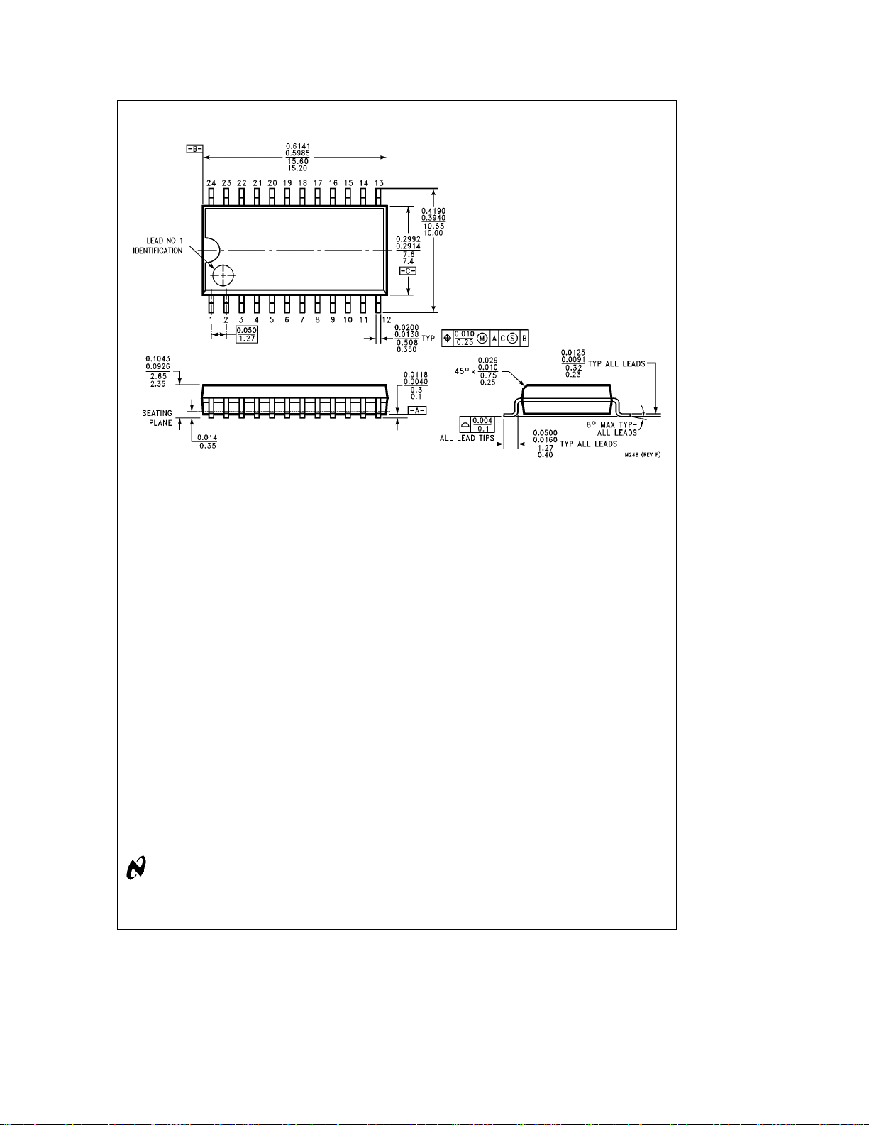
Physical Dimensions inches (millimeters) unless otherwise noted
LMC6008 8 Channel Buffer
24-Lead (3.00×Wide) Small Outline Molded Package (M)
Order Number LMC6008IM or LMC6008IMX
NS Package Number M24B
LIFE SUPPORT POLICY
NATIONAL’S PRODUCTS ARE NOT AUTHORIZED FOR USE AS CRITICAL COMPONENTS IN LIFE SUPPORT
DEVICES OR SYSTEMS WITHOUT THE EXPRESS WRITTEN APPROVAL OF THE PRESIDENT OF NATIONAL
SEMICONDUCTOR CORPORATION. As used herein:
1. Life support devices or systems are devices or 2. A critical component is any component of a life
systems which, (a) are intended for surgical implant support device or system whose failure to perform can
into the body, or (b) support or sustain life, and whose be reasonably expected to cause the failure of the life
failure to perform, when properly used in accordance support device or system, or to affect its safety or
with instructions for use provided in the labeling, can effectiveness.
be reasonably expected to result in a significant injury
to the user.
National Semiconductor National Semiconductor National Semiconductor National Semiconductor
Corporation Europe Hong Kong Ltd. Japan Ltd.
1111 West Bardin Road Fax:
Arlington, TX 76017 Email: europe.support@nsc.com Ocean Centre, 5 Canton Rd. Fax: 81-043-299-2408
Tel: 1(800) 272-9959 Deutsch Tel:
Fax: 1(800) 737-7018 English Tel:
http://www.national.com
National does not assume any responsibility for use of any circuitry described, no circuit patent licenses are implied and National reserves the right at any time without notice to change said circuitry and specifications.
Fran3ais Tel:
Italiano Tel:a49 (0) 180-534 16 80 Fax: (852) 2736-9960
a
49 (0) 180-530 85 86 13th Floor, Straight Block, Tel: 81-043-299-2308
a
49 (0) 180-530 85 85 Tsimshatsui, Kowloon
a
49 (0) 180-532 78 32 Hong Kong
a
49 (0) 180-532 93 58 Tel: (852) 2737-1600
 Loading...