

查询LMC1982供应商
LMC1982
Digitally-Controlled Stereo Tone and Volume Circuit with
Two Selectable Stereo Inputs
General Description
The LMC1982 is a monolithic integrated circuit that provides
volume, balance, tone (bass and treble), enhanced stereo,
and loudness controls and selection between two pairs of
stereo inputs. These functions are digitally controlled
through a three-wirecommunicationinterface. There are two
digital inputs for easy interface to other audio peripherals
such as stereo decoders. The LMC1982 is designed for line
level input signals (300 mV–2V) and has a maximum gain of
−0.5 dB. Volumeis set at minimum and tone controls are flat
when supply voltage is first applied.
Low noise and distortion result from using analog switches
and poly-silicon resistor networks in the signal path.
Additional tone control can be achieved using the LMC835
stereo 7-band graphic equalizer connected to the
LMC1982’s SELECT OUT/SELECT IN external processor
loop.
Features
n Low noise and distortion
n Two pairs of stereo inputs
December 1994
n Enhanced stereo function
n Loudness compensation
n 40 position 2 dB/step volume attenuator plus mute
n Independent left and right volume controls
n Low noise-suitable for use with DNR
reduction
n External processor loop
n Signal handling suitable for compact discs
n Pop-free switching
n Serially programmable: INTERMETAL bus (IM) interface
n 6V to 12V single supply operation
n 28 Pin DIP or PLCC package
®
and Dolby®noise
Applications
n Stereo television
n Music reproduction systems
n Sound reinforcement systems
n Electronic music (MIDI)
n Personal computer audio control
LMC1982 Digitally-Controlled Stereo Tone and Volume Circuit with Two Selectable Stereo Inputs
Block and Connection Diagrams
DS011028-1
DNR®is a registered trademark of National Semiconductor Corporation.
®
Dolby
is a registered trademark of Dolby Labs.
© 1999 National Semiconductor Corporation DS011028 www.national.com
Absolute Maximum Ratings (Notes 1, 2)
If Military/Aerospace specified devices are required,
please contact the National Semiconductor Sales Office/
Distributors for availability and specifications.
Supply Voltage (V
Voltage at any Pin GND − 0.2V to V
Input Current at any Pin (Note 3) 5 mA
Package Input Current (Note 3) 20 mA
Power Dissipation (Note 4) 500 mW
Junction Temperature +125˚C
Storage Temperature −65˚C to +150˚C
Lead Temperature
+
− GND) 15V
+
0.2V
N Package,
(Soldering, 10 Seconds) +260˚C
V Package,
(Vapor Phase, 60 Seconds) 215˚C
Infrared, (15 Seconds) 220˚C
ESD Susceptability (Note 5) 2 kV
+
Operating Ratings(Notes 1, 2)
Temperature Range T
LMC1982CIN, LMC1982CIV −40˚C ≤ TA≤ +85˚C
Supply Voltage Range (V
+−V−
) 6Vto12V
MIN
≤ TA≤ T
MAX
Electrical Characteristics
The following specifications apply for V
0 dB, treble=0 dB, enhanced stereo is off, and loudness is off unlessotherwise specified. All limits apply for T
+
=
=
9V, f
1 kHz, input signal (300 mV) applied to INPUT 1, volume=0 dB, bass
IN
=
=
T
+25˚C.
A
J
Symbol Parameter Conditions Typical Limit Unit
(Note 6) (Note 7) (Limit)
I
V
Supply Current 15 25 mA (max)
S
Input Voltage Clipping Level (1,.0%THD), 2.3 2.0 V
IN
rms
Select Out (Pins 6, 23)
THD Total Harmonic Distortion Left and Right channels;
Output Pins 13, 16
=
V
0.3 V
IN
V
IN
V
IN
V
IN
rms
=
f
100 Hz, 1 kHz, 10 kHz
IN
=
2.0 V
rms
=
f
100 Hz, 1 kHz
IN
=
2.0 V
rms
=
f
10 kHz
IN
=
0.5 V
rms
; 0.008 0.1
; 0.4 1.0
; 0.5 1.0
; Bass and Treble 0.07 0.5
%
%
%
%
(max)
(max)
(max)
(max)
Tone Controls Set at Maximum
=
V
IN
Attenuator at −20 dB, Bass and Treble 0.06 0.15
0.3 V
; Volume
rms
%
(max)
Tone Controls Set at Maximum
DC Shifts V
=
IN
; Between Any 2.0 4.0 mV (max)
0.3 V
rms
Two Adjacent Control Settings
=
V
IN
; 18 20 mV (max)
0.3 V
rms
All Mode and Input Positions
R
AC Output Impedance Pins 6, 23, (470Ω to Ground at Input) 150 200 Ω (max)
OUT
Pins 13, 16 26 40 Ω (max)
R
AC Input Impedance Pins 4, 5, 24, 25 50 72 kΩ (max)
IN
35 kΩ (min)
Volume Attenuator Range Pins 13, 16; Volume 0.5 1.5 dB (max)
Attenuation at 0100010XXX000000 (0 dB)
0100010XXX101XXX (80 dB); 80 78 dB (min)
(Relative to Attenuation at 82 dB (max)
the 0 dB Setting)
Volume Step Size All Volume Attenuation Settings
from 0100010XXX101XXX (80 dB) to 2.0 1.5 dB (min)
0100010XXX000000 (0 dB) (Note 9) 2.5 dB (min)
=
(min)
www.national.com 2
Electrical Characteristics (Continued)
+
=
The following specifications apply for V
0 dB, treble=0 dB, enhanced stereo is off, and loudness is off unlessotherwise specified. All limits apply for T
Symbol Parameter Conditions Typical Limit Unit
Channel-to-Channel Volume All Volume Attenuation Settings
Tracking Error from 0100010XXX101XXX (80 dB)
Mute Attenuation V
Bass Gain Range f
Bass Tracking Error f
Bass Step Size f
Treble Gain Range f
Treble Tracking Error f
Treble Step Size f
Enhanced Stereo Cross
Coupling
Frequency Response V
Loudness Volume Attenuator=40 dB, Loudness
Signal-to-Noise Ratio V
Channel Balance All Volume Settings 0.2 1.0 dB (max)
Channel Separation Input Pins 4, 25: Output Pins 13, 16; 80 60 dB (min)
Input-Input Isolation 470Ω to AC Ground on Unused Input 95 60 dB (min)
PSSR Power Supply Rejection Ratio V
f
V
V
V
V
Clock Frequency 5.0 1.0 MHz
CLK
Logic “1” Input Voltage Pins 1, 27, 28 (IM Bus) 1.3 2.0 V (min)
IN(1)
Logic “0” Input Voltage Pins 1, 27, 28 (IM Bus) 0.4 0.8 V (max)
IN(0)
Logic “1” Output Voltage Pin 28 (IM Bus) 2.0 V (min)
OUT(1)
Logic “0” Output Voltage Pin 28 (IM Bus) 0.4 0.8 V (max)
OUT(0)
Note 1: AbsoluteMaximum Ratings indicate limits beyond which damage to the deivce may occur. Operating Ratings indicate conditions for which the device is functional, but do not guarantee specific performance limits. For guaranteed specifications and test conditions, see the Electrical Characteristics. The guaranteed specifications apply only for the test conditions listed. Some performance characteristics may degrade when the device is not operated under the listed test conditions.
Note 2: All voltages are specified with respect to ground.
Note 3: When the input voltage (V
limited to 5 mA or less. The 20 mA package input current limits the number of pins that can exceed the power supply voltages with 5 mA current limit to four.
) at any pin exceeds the power supply voltages (V
IN
=
9V, f
1 kHz, input signal (300 mV) applied to INPUT 1, volume=0 dB, bass
IN
=
=
T
+25˚C.
A
J
(Note 6) (Note 7) (Limit)
±
0.1
±
1.5 dB (min)
to 0100010XXX000000 (0 dB)
=
1.0 V
IN
IN
IN
IN
rms
=
100 Hz, Pins 13, 16
=
100 Hz, Pins 13, 16
=
100 Hz, Pins 13, 16 2.0 1.5 dB (min)
105 86 dB (max)
±
12
±
0.1
±
10.0 dB (min)
±
14.0 dB (max)
±
1.5 dB (max)
(Relative to Previous Level) 2.5 dB (max)
=
10 kHz, Pins 13, 16
IN
=
10 kHz, Pins 13, 16
IN
=
10 kHz, Pins 13, 16 2.0 1.5 dB (min)
IN
±
12
±
0.1
±
10.0 dB (min)
±
14.0 dB (max)
±
1.5 dB (max)
(Relative to Previous Level) 2.5 dB (max)
(Note 10) −4.4 −2.5 dB (min)
−6.9 dB (max)
Applied to Input 1 and Input 2;
IN
=
f
20 Hz − 20 kHz
IN
±
0.1
±
1.0 dB (max)
(Relative to Signal Amplitude at 1 kHz)
on (See
Figure 5
)
Gain at 100 Hz (Referenced 11.5 13.5 dB (max)
to Gain at 1 kHz) 9.5 dB (min)
Gain at 10 kHz (Referenced 6.5 8.5 dB (max)
to Gain at 1 kHz) 4.5 dB (min)
=
IN
Measured at 1 kHz, R
=
V
IN
+
=
, A Weighted, 95 90 dB (min)
1.0 V
1.0V
9V
rms
rms
; 200 mV
DC
(Note 8)
=
470Ω
S
, 100 Hz 32 28 dB (min)
rms
Sinewave Applied to Pin 26
(max)
Pins 2, 3 2.9 5.5 V (min)
Pins 2, 3 1.2 3.5 V (max)
<
IN
V−or V
>
V+) the absolute value of the current at that pin should be
IN
=
www.national.com3
Electrical Characteristics (Continued)
Note 4: The maximum power dissipation must be derated at elevated temperatures and is dictated by T
allowable power dissipation is P
+125˚C, and the typical junction-to-ambient thermal resistance, when board mounted, is 67˚C/W.
Note 5: Human body model; 100 pF discharged through a 1.5 kΩ resistor.
Note 6: Typicals are at T
Note 7: Limits are guaranteed to National’s AOQL (Average Outgoing Quality Level).
Note 8: The Input-Input Isolation is tested by driving one input and measuring the output when the undriven input are selected.
Note 9: TheVolumeStepSize is defined as the change in attenuation between any two adjacent volume attenuation settings. The nominalVolumeStep Size is 2 dB.
Note 10: Enhanced Stereo Cross Coupling is a measure of the ratio between the undriven right channel output signal and the driven left channel output signal. It
is measured by driving the left inputs with a 300 mV
=
(T
D
=
+25˚C and represent the most likely parametric norm.
J
)/θJAor the number given in the Absolute Maximum Ratings, whichever is lower. For the LMC1982CIN, T
JMAX−TA
signal while the right inputs are grounded.
rms
, θJA, and the ambient temperature TA. The maximum
JMAX
JMAX
Typical Performance Characteristics
=
Supply Current
vs Supply Voltage
THD vs
Load Impedance
THD vs V
(V
OUT
IN
Constant)
DS011028-13
DS011028-16
Output Voltage
vs Supply Voltage
CCIR Output Noise
vs Volume Setting
THD vs Frequency
DS011028-14
DS011028-17
THD vs
Load Impedance
DS011028-15
Channel Separation
vs Frequency
DS011028-18
Mute Gain
vs Frequency
DS011028-19
www.national.com 4
DS011028-20
DS011028-21
Typical Performance Characteristics (Continued)
Tone Control Response
with Equal Bass and
Treble Control Settings
DS011028-22
Loudness Response
vs Frequency
DS011028-23
Select Input Impedance
vs Frequency
DS011028-24
www.national.com5

Connection Diagrams
DS011028-2
Top View
Order Number LMC1982CIN
See NS Package Number N28B
Pin Description
CLK (1) The INTERMETAL (IM) Bus clock is applied
DIGITAL INPUT
1 & 2 (2, 3)
INPUTS1&2
(4, 25; 5, 24)
SELECT OUT
(6, 23)
SELECT IN
(7, 22)
TONE IN
(8, 21)
TONE OUT
(9, 20)
OP AMP
OUT (10, 19)
to the CLOCK pin. This input accepts a TTL
or CMOS level signal. The input is used to
clock the DATA signal. A data bit must be
valid on the rising clock edge.
Internally tied high to V
+
through a 30 kΩ
pull-up resistor, these inputs allow a peripheral device to place any single-bit, active low
digital information onto the IM Bus. It is then
sent out to the controlling device through the
DATA pin. Examples of such information
could include indication of the presence of a
Second Audio Program (SAP) or an FM stereo carrier.
These are the LMC1982’s two stereo input
pairs.
The selected INPUT signal is available at this
output. This feature allows external signal
processors such as noise reduction or
graphic equalizers to be used. This output
can typically sink 1 mA. These pins should be
capacitively coupled to pins 7 and 22, respectively, if no external processor is used.
These are the inputs that an external signal
processor uses to return a signal to the
LMC1982. These pins should be capacitively
coupled to pins 6 and 23, respectively, if no
external processor is used.
These are the inputs to the tone control amplifier. See the Application Information section titled “Tone Control Response”.
Tone control amplifier output. See the Application Information section titled “Tone Control
Response”.
These outputs are used with external tone
control capacitors. Internally, this output is
applied to the volume attenuators.
DS011028-12
Top View
Order Number LMC1982CIV
See NS Package Number V28A
LOUDNESS
(11, 18)
The output signal on these pins is a voltage
taken from the volume attenuator’s −40 dB
tap point. An external R–C network is connected to these pins.
ENHANCED
STEREO
(12, 17)
An external R–C network is connected
across these pins. This provides left-right
channel cross-coupling and cancellation to
create an enhanced stereo channel separation effect.
MAIN
OUTPUT
(13, 16)
The output signal from these pins drives a
stereo power amplifier. The output can typically sink 1 mA.
BYPASS (14) A 10 µF capacitor is connected between this
pin and ground to provide an AC ground for
the internal half-supply voltage reference.
GROUND (15)This pin is connected to analog ground.
+
V
(26) This is the power supply connection. The
LMC1982 is operational with supply voltages
from 6V to 12V.This pin should be bypassed
to ground through a 1.0 µF capacitor.
ID (27) This is the IDENTITY digital input that, when
low, signals the LMC1982 to receive, from a
controlling device, a device address
(40
–47H), present on the DATA line.
H
DATA (28) This is the serial data input for communica-
tions sent by a controller.The controller must
have open drain outputs used with external
pull-up resistors. The data rate has a maximum frequency of 1 MHz. The LMC1982 requires 16 bits of data to control or change a
function: the first 8 bits select the LMC1982
and one of eight functions. The final eight bits
set the function to a desired value. The data
must be valid on the rising edge of the
CLOCK input signal.
www.national.com 6

Pin Description (Continued)
TABLE 1. IM Bus Programming Codes for LMC1982
Address Function Data Function
(A7–A0) Selected
01000000 Input Select + Mute XXXXXX00 INPUT1
01000001 Loudness, Enhanced Stereo XXXXXX00 Loudness OFF
01000010 Bass XXXX0000 −12 dB
01000011 Treble XXXX0000 −12 dB
01000100 Left Volume XX000000 0 dB
01000101 Right Volume XX000000 0 dB
01000110 Mode Select XXXXX100 Left Mono
01000111 Read Digital Input 1 XXXXXXD1D0 D0=Digital Input 1
XXXXXX01 INPUT2
XXXXXX10 N/A
XXXXXX11 MUTE
Enhanced Stereo OFF
XXXXXX01 Loudness ON
Enhanced Stereo OFF
XXXXXX10 Loudness OFF
Enhanced Stereo ON
XXXXXX11 Loudness ON
Enhanced Stereo ON
XXXX0011 −6 dB
XXXX0110 FLAT
XXXX1001 +6 dB
XXXX11XX +12 dB
XXXX0011 −6 dB
XXXX0110 FLAT
XXXX1001 +6 dB
XXXX11XX +12 dB
XX010100 −40 dB
XX101XXX −80 dB
XX11XXXX −80 dB
XX010100 −40 dB
XX101XXX −80 dB
XX11XXXX −80 dB
XXXXX101 Stereo
XXXXX11X Right Mono
or D1=Digital Input 2
Digital Input 2
on IM Bus
General Information
The LMC1982 is a CMOS/bipolar building block intended for
high fidelity audio signal processing. It is designed for line
level inputs signals (300 mV − 2V) and has a maximum gain
of −0.5 dB. While the LMC1982 is manufactured with CMOS
processing, NPN transistors are used to build low noise op
amps. The combination of CMOS switches, bipolar op amps,
and poly-silicon resistors make it possible to achieve an order of magnitude quality improvement over other bipolar circuits that use analog multipliers to accomplish gain adjustment. Internal circuits set the volume to minimum, tone
controls to flat, the mute to on, and all other functions off
when power is first applied. Individual left and right volume
controls are software programmed to achieve the stereo balance function.
typical LMC1982 application.
The LMC1982 has internal decoding logic that allows a microprocessor (µP) or microcontroller (µC) to communicate directly to the audio control circuitry through an INTERMETAL
(IM) Bus interface. This three-wire interface consists of a
bi-directional DATA line, a Clock (CLK) input line, and an
Identity (ID) line. Address and function selection data (8 bits)
Figure 1
shows the connection diagram of a
www.national.com7

General Information (Continued)
are serially shifted from the controller to the LMC1982. This
is followed by 8 bits of function value data. Data present in
the internal shift register is latched and the instruction is
executed.
FIGURE 1. Typical Application
Application Information
INPUT SELECTOR
The LMC1982’s input selector and mode control are shown
in
Figure 2
nal sources or a mute function with typical attenuation of
100 dB. The selected signals are then sent to a mode control
matrix. As shown in
reo or can direct either channel to both LEFT or RIGHT SELECT OUTPUTs. The third matrix mode is normal stereo.
The control matrix output is buffered and appears on each
channel’s respective SELECT OUT pin (6, 23). Switching
noise is kept to a minimum when mute is selected by using
a50kΩbias resistor.
Noise performance is optimized through the use of emitter
followers in the mode control matrix’s output. Internal 50 kΩ
resistors are connected to each input selector pin to provide
the proper bias point for the emitter follower buffers. Each internal 50 kΩ bias resistor is connected to a common
half-supply (V
and 23 (SELECT OUT) that is 1.4V below V
3.1V with V
put pins (4, 5, 24, and 25), input signal should be AC coupled
through a 1 µF capacitor.
www.national.com 8
. The input selector selects one of two stereo sig-
Table1
, the matrix provides normal ste-
+
/2) source. This produces a voltage at pins 6
+
=
9V). Since a DC voltage is present at the in-
+
/2 (typically
DS011028-5
The output signal at pins 6 and 23 can be used to drive exteral audio processing circuits such as noise reduction
(LM1894–DNR or Dolby) or graphic equalizers (LMC835). It
is important that if any noise reduction is used it be placed
ahead of any tone controls or equalizers in the external circuit path to preserve the frequency spectrum of the selected
input signal. Otherwise, any frequency equalization could
prevent the proper operation of the noise reduction circuit. If
no external processor is used, a capacitor should be used to
couple the SELECT OUT signals directly to pins 7 and 22,
respetively.
MINIMUM LOAD IMPEDANCE
The LMC1982 employs emitter-followers to buffer the selected stereo channels. The buffered signals are available at
pins 6 and 23 (SELECT OUT). The SELECT OUT buffers operate with a typical bias current 1 mA.
The Electrical Specifications table lists a maximum input signal of 2.0 V
pins. This distortion level is achieved when the minimum AC
(2.5 V
rms
) for 1%THD at the SELECT OUT
peak
load impedance seen by the SELECT OUT pins is 2.5 kΩ
(2.5V/1 mA). Using lower load impedances results in clipping
at lower output levels. If the load impedance is DC-coupled,
an increased quiescent current can flow.Latch-up may occur

Application Information (Continued)
if the total emitter current exceeds 5 mA. Thus, maximum
output voltage can be increased and much lower distortion
levels can be achieved using load impedances of at least
25 kΩ.
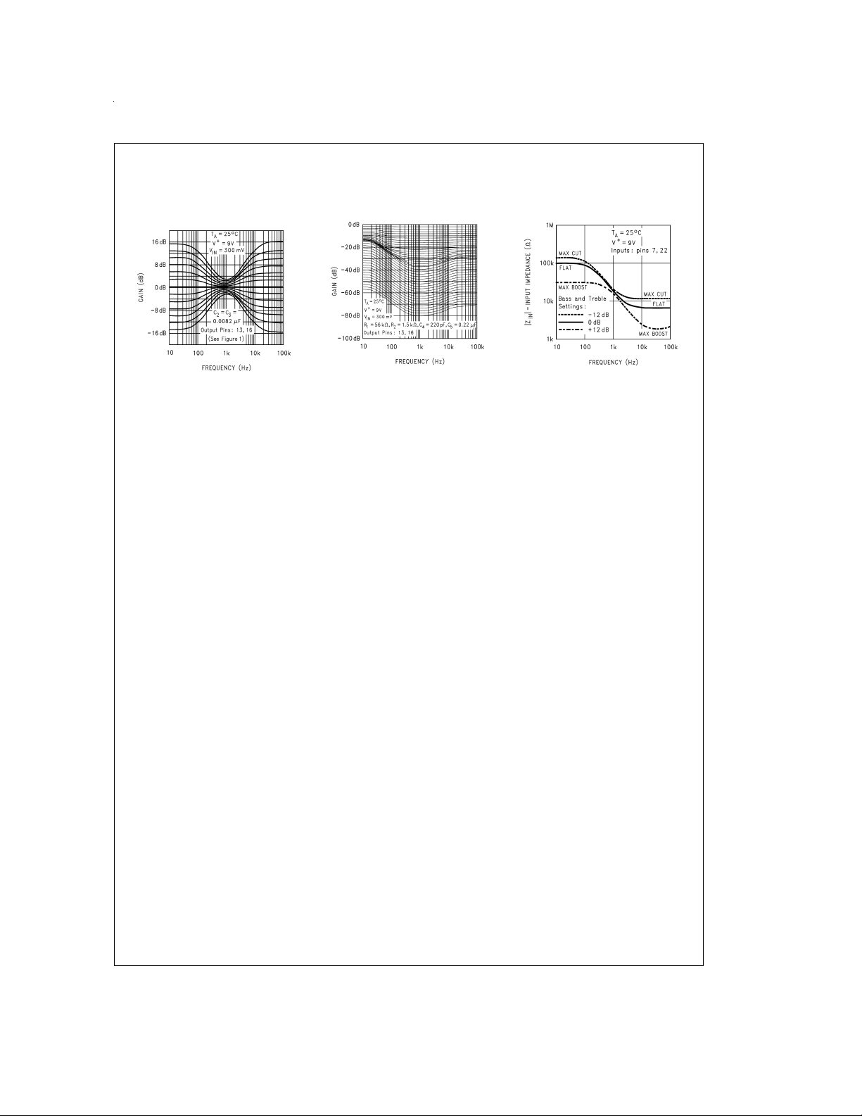
INPUT IMPEDANCE
The input impedance of pins 4, 5, 24 and 25 is defined by internal bias resistors and is typically 50 kΩ.
The SELECT IN pins have an input impedance that varies
with the BASE and TREBLE control settings. The input impedance is 100 kΩ at DC and 19 kΩ at 1 kHz when the controls are set at 0 dB. Minimum input impedance of 30.4 kΩ at
DC and 16 kΩ at 1 kHz occurs when maximum boost is selected. At 10 kHz the minimum input impedance, with the
tone controls flat, is 6.8 kΩ and, with the tone controls at
maximum boost, is 2.5 kΩ.
FIGURE 2. Input and Mode Select Circuitry
EXTERNAL SIGNAL PROCESSING
The SELECT OUT pins (6 and 23) enable greater system
design flexibility by providing a means to implement an external processing loop. This loop can be used for noise reduction circuits such as DNR (LM1894) or multi-band
graphic equalizers (LMC835). If both are used, it is important
to ensure that the noise reduction circuitry precede the
equalization circuits. Failure to do so results in improper operation of the noise reduction circuits. The system shown in
Figure 3
multi-band equalizer.
TONE CONTROL RESPONSE
Bass and treble tone controls are included in the LMC1982.
The tone controls used just two external capacitors for each
stereo channel. Each has a corner frequency determined by
the value of C2 and C3 (see
in the feedback loop of the internal tone amplifier. The
maximum-boost or cut is determined by the data sent to the
LMC1982 (see
The typical tone control response shown in Typical Performance Curves were generated with C2=C3=0.0082 µF
and show the response for each step. When modifying the
utilizes the external loop to include DNR and a
Figure 4
) and internal resistors
Table 1
).
DS011028-6
tone control response it is important to note that the ratio of
C3 and C2 sets the mid-frequency gain. Symmetrical tone
response is achieved when C2=C3. However, with
C2=2(C3) and the tone controls set to “flat”, the frequency
response will be flat at 20 Hz and 20 kHz, and +6 dB at
1 kHz.
The frequency where a tone control begins to deviate from a
flat response is referred to as the turn-over frequency. With
C=C2=C3, the LMC1982’s treble turn-over frequency is
nominally
www.national.com9

Application Information (Continued)
The bass turn-over frequency is nominally
when maximum boost is chosen. The inflection points (the
frequencies where the boost or cut is within 3 dB of the final
value) are for treble and bass
FIGURE 3. System Block Diagram Utilizing the External Processing Loop (One Channel Shown)
DS011028-8
FIGURE 4. The Tone Control Amplifier
Increasing the values of C2 and C3 decreases the turnover
and inflection frequencies: i.e., the Tone Control Response
Curves shown in Typical Performance Curves will shift left
when C2 and C3 are increased and shift right when C2 and
C3 are decreased. With C2=C3=0.0082 µF, 2 dB steps
are achieved at 100 Hz and 10 kHz. Changing C2 and C3 to
0.01 µF shifts the 2 dB per step frequency to 72 Hz and
www.national.com 10
DS011028-7
8.3 kHz. If the tone control capacitors size is decreased
these frequencies will increase. With C2=C3=0.0068 µF
the 2 dB steps take place at 130 Hz and 11.2kHz.
LOUDNESS
The human ear has less sensitivity to high and low frequencies relative to its sensitivity to mid-range frequencies between 2 kHz and 6 kHz for any given acoustic level. The low
and high frequency sensitivity decreases faster than the sensitivity to the mid-range frequencies as the acoustic level
drops. The LMC1982’s loudness function can be used to
help compensate for the decreased sensitivity by boosting
the gain at low and high frequencies as the volume control
attenuation increases (see the curve labeled “Gain vs Frequency with Loudness Active”).
The LMC1982’s loudness function uses external components R1, R2, C4 and C5, as shown in
Figure 5
, to select the
frequencies where bass and treble boost begin. The amount
of boost is dependent on the volume attenuator’s setting.
The loudness characteristic, with the volume attenuator set
at 40 dB, has a transfer function of
The external components R1 and C4 can be eliminated and
pin 10(19) left open if bass boost is the only desired loudness characteristic.

Application Information (Continued)
As shown in
controlled through the same address. It is important to remember to set both functions to the correct value any time
either of these functions is updated.
ENHANCED STEREO
The LMC1982 has an enhanced stereo effect that can be
achieved by cross-coupling reverse phase information between the left and right stereo channels. This feature can
help improve the apparent stereo channel separation when,
because of cabinet or equipment limitations, the left and right
speakers are closer to each other than optimum.
Enhanced stereo is created by connecting an external frequency shaping RC network between the OUTPUT operational amplifiers’ inverting inputs through an internal CMOS
switch (see
each channel’s output to the opposite channel’s inverting input. This cancels a portion of the signal common to both
channels.
The desired 60%cross-coupling is accomplished through
the internal 6.5 kΩ feedback resistor and an external 10 kΩ
resistor.Bass frequency cancellation is prevented by using a
0.047 µF coupling capacitor to couple only frequencies
above 330 Hz. Switching noise is eliminated by using a
680 kΩ resistor across the 0.047 µF. R3, R4 and C6 can be
eliminated if enhanced stereo is not desired.
As shown in
controlled through the same address. It is important to remember to set both functions to the correct value any time
either of these functions is updated.
SERIAL DATA COMMUNICATION
The LMC1982 uses the INTERMETAL serial bus (IM Bus)
standard. Serial data information is sent to the LMC1982
over a three wire IM Bus consisting of Clock (CLK), Data
(DATA), and Identity (ID). The DATA line is bidirectional and
the CLK and ID lines are unidirectional from the microprocessor or micontroller to the LMC1982. The LMC1982’s bidi-
Table 1
, loudness and enhanced stereo are
DS011028-9
FIGURE 5. Loudness Control Circuit
Figure 6
). The external network couples 60%of
DS011028-10
FIGURE 6. Enhanced Stereo Circuit
Table 1
, enhanced stereo and loudness are
rectional capability is accomplished by using an open drain
output on the DATAline and an external 1 kΩ pull-up resistor.
The LMC1982 responds to address values from 01000000
(40
) through 01000111 (47H). The addresses select one of
H
the eight available functions (see
Table1
). The IM Bus’ lines
have a logic high standby state when using TTL logic levels.
As shown in
Figure 7
, data transmission is initiated by low
levels on CLK and ID. Next, eight address bits are sent. This
address information includes the code to select one of the
LMC1982’s desired functions. Each address bit is clocked in
on the rising edge of CLK. The ID line is taken high after the
eight bits of address data are received by the LMC1982. The
controlling system continues toggling the CLK line eight
more times. Data that determines the selected function’s operating point is written into, or single bit information on DIGITAL INPUT 1 or DIGITAL INPUT 2 is read from, the
LMC1982. Finally, the end of transmission is signalled by
pulsing the ID line low for a minimum of 1 µs. The transmitted function data is latched and the function changes to its
new setting.
Table 1
also details the serial data structure, range, and bit
assignments that sets each function’s operating point. The
volume and tone controls’ function control data binarily increments from zero to maximum as the function’s operating
point changes from 80 dB attenuation to 0 dB attenuation
(volume) or −12 dB to +12 dB (tone controls). Note that not
all data bits are needed by each function. The extra bits
shown as “X”s (“don’t cares”) are position holders and have
no affect on a respective function. They are necessary to
properly position the data in the LMC1982’s internal data
shift register. Unexpected results may take place if these bits
are not sent.
The LMC1982’s internal data shift register can handle either
a 16-bit word or two 8-bit serial data transmissions. It is the
final 8 bits of data received before the ID line goes high that
are used as the LMC1982 selection and function addresses.
The final eight bits after the ID line returns high are used to
change a function’s operating point. CLK must be stopped
when the final 8 data bits are received. The data stored in the
internal data latch remains unchanged until the ID is pulsed,
signifying the end of data transmission. When ID is pulsed,
the new data in the data shift register is latched into the data
latch and the selected function takes on a new operating
point.
A complete description and more information concerning the
IM Bus is given in the appendix of ITT’s CCU2000
datasheet.
DIGITAL I/O
The LMC1982’s two Digital Input pins, 2 and 3, provide
single-bit communication between a peripheral device and
the controller over the IM Bus. Each pin has an internal
30 kΩ pull-up resistor. Therefore, these pins should be connected to open collector/drain outputs. The type of information that could be received on these lines and retrieved by a
controller include FM stereo pilot indication, power on/off,
Secondary Audio Program (SAP), etc.
According to
Table1
, the logic state of DIGITALINPUT1 and
DIGITALINPUT2 is latched and can be retrieved over the IM
Bus using the read command (47
tion sent on the IM Bus is active low since these lines are in-
). The single-bit informa-
H
ternally pulled high.
www.national.com11

Application Information (Continued)
FIGURE 7. LMC1982’s INTERMETAL Serial Bus Timing
DS011028-11
www.national.com 12

Physical Dimensions inches (millimeters) unless otherwise noted
Order Number LMC1982CIN
NS Package Number N28B
www.national.com13

Physical Dimensions inches (millimeters) unless otherwise noted (Continued)
Order Number LMC1982CIV
NS Package Number V28A
LIFE SUPPORT POLICY
NATIONAL’S PRODUCTS ARE NOT AUTHORIZED FOR USE AS CRITICAL COMPONENTS IN LIFE SUPPORT
DEVICES OR SYSTEMS WITHOUT THE EXPRESS WRITTEN APPROVAL OF THE PRESIDENT AND GENERAL
COUNSEL OF NATIONAL SEMICONDUCTOR CORPORATION. As used herein:
1. Life support devices or systems are devices or
systems which, (a) are intended for surgical implant
into the body, or (b) support or sustain life, and
whose failure to perform when properly used in
accordance with instructions for use provided in the
2. A critical component is any component of a life
support device or system whose failure to perform
can be reasonably expected to cause the failure of
the life support device or system, or to affect its
safety or effectiveness.
labeling, can be reasonably expected to result in a
significant injury to the user.
National Semiconductor
Corporation
Americas
Tel: 1-800-272-9959
Fax: 1-800-737-7018
Email: support@nsc.com
LMC1982 Digitally-Controlled Stereo Tone and Volume Circuit with Two Selectable Stereo Inputs
www.national.com
National does not assume any responsibility for use of any circuitry described, no circuit patent licenses are implied and National reserves the right at any time without notice to change said circuitry and specifications.
National Semiconductor
Europe
Fax: +49 (0) 1 80-530 85 86
Email: europe.support@nsc.com
Deutsch Tel: +49 (0) 1 80-530 85 85
English Tel: +49 (0) 1 80-532 78 32
Français Tel: +49 (0) 1 80-532 93 58
Italiano Tel: +49 (0) 1 80-534 16 80
National Semiconductor
Asia Pacific Customer
Response Group
Tel: 65-2544466
Fax: 65-2504466
Email: sea.support@nsc.com
National Semiconductor
Japan Ltd.
Tel: 81-3-5639-7560
Fax: 81-3-5639-7507
 Loading...