

Page 1
LM97593
Dual ADC / Digital Tuner / AGC
LM97593 Dual ADC / Digital Tuner / AGC
March 12, 2008
General Description
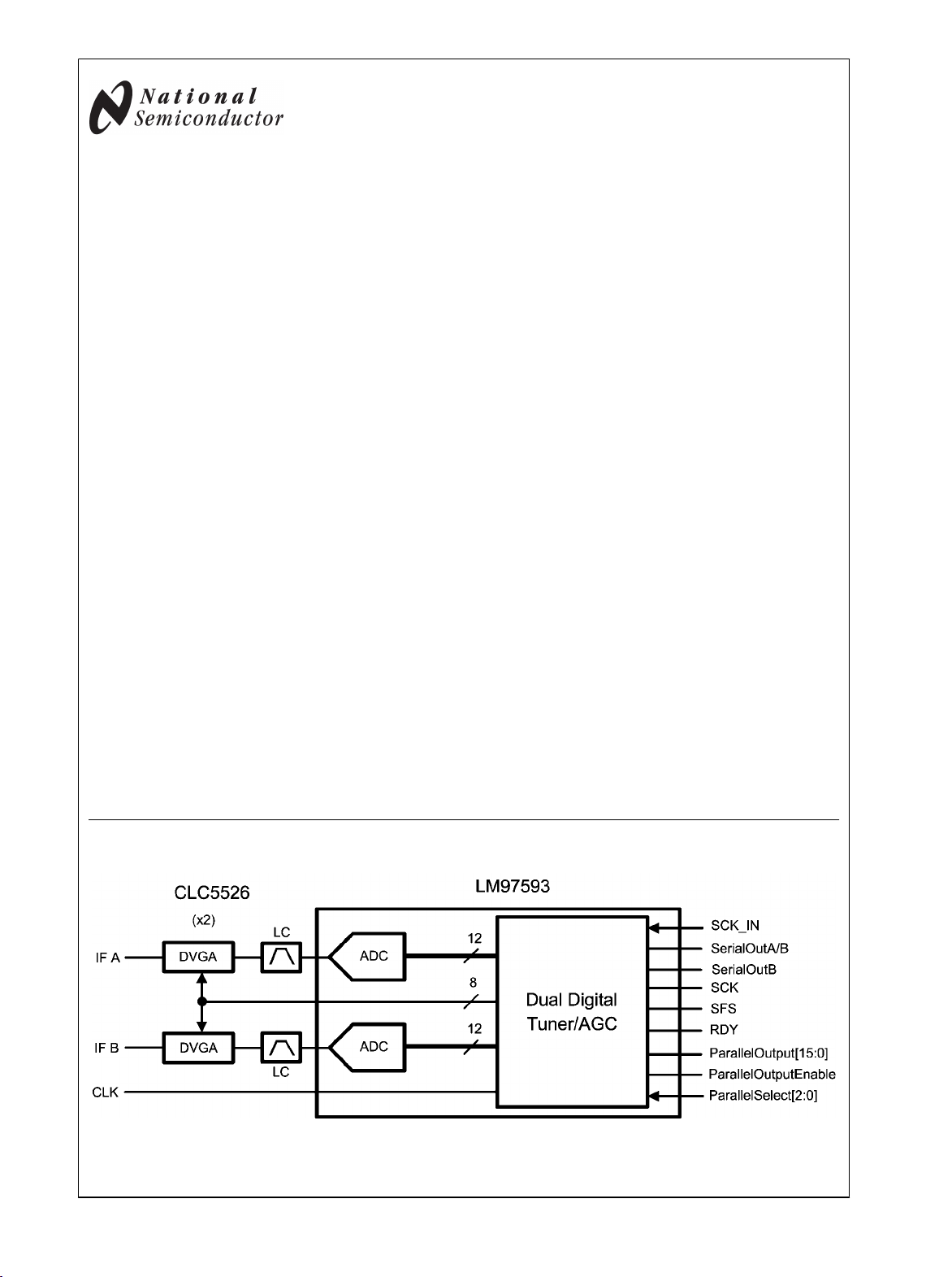
The LM97593 Dual ADC / Digital Tuner / AGC IC is a two
channel digital downconverter (DDC) with integrated 12-bit
analog-to-digital converters (ADCs) and automatic gain control (AGC). The LM97593 further enhances National’s Diversity Receiver Chipset (DRCS) by integrating a wide-bandwidth dual ADC core with the DDC. The complete DRCS
includes one LM97593 Dual ADC / Digital Tuner / AGC and
two CLC5526 digitally controlled variable gain amplifiers (DVGAs). This system allows direct IF sampling of signals up to
300MHz for enhanced receiver performance and reduced
system costs. A block diagram for a DRCS-based narrowband communications system is shown in Figure 1.
The LM97593 offers high dynamic range digital tuning and
filtering based on hard-wired digital signal processing (DSP)
technology. Each channel has independent tuning, phase offset, filter coefficients, and gain settings. Channel filtering is
performed by a series of three filters. The first is a 4-stage
Cascaded Integrator Comb (CIC) filter with a programmable
decimation ratio from 8 to 2048. Next there are two symmetric
FIR filters, a 21-tap and a 63-tap, both with independent programmable coefficients. The first FIR filter decimates the data
by 2, the second FIR decimates by either 2 or 4. Channel filter
bandwidth at 52MSPS ranges from ±650kHz down to
±1.3kHz. At 65MSPS, the maximum bandwidth increases to
±812kHz.
The LM97593’s AGC controller monitors the ADC output and
controls the ADC input signal level by adjusting the DVGA
setting. AGC threshold, deadband+hysteresis, and the loop
time constant are user defined. Total dynamic range of
greater than 123dB full-scale signal to noise in a 200kHz
bandwidth can be achieved with the Diversity Receiver
Chipset.
Features
100% Software compatible with the CLC5903
■
Pin compatible with the CLC5903 except for the analog
■
input and reference section
123 dB dynamic range with CLC5526 DVGA (200kHz)
■
On-chip precision reference
■
User Programmable AGC with enhanced Power Detector
■
Channel Filters include a Fourth Order CIC followed by 21-
■
tap and 63-tap Symmetric FIRs
Flexible output formats
■
Serial and Parallel output ports
■
JTAG Boundary Scan
■
8-bit Microprocessor Interface
■
128 pin PQFP
■
Key Specifications
Internal ADC Resolution 12 Bits
■
Sample Rate 65 MSPS
■
SNR (fIN = 250MHz, 11-bit, Nyquist) 62 dBFS (typ)
■
SNR (fIN = 250MHz, 200kHz) 83 dBFS (typ)
■
SFDR (fIN = 250MHz, 11-bit, Nyquist) 68 dBFS (typ)
■
Full Power Bandwidth 650 MHz (typ)
■
Power Consumption (65MSPS) 560 mW (typ)
■
Applications
Cellular Basestations
■
GSM / GPRS / EDGE / GSM Phase 2 Receivers
■
Satellite Receivers
■
Wireless Local Loop Receivers
■
Digital Communications
■
Block Diagram 1
30008701
FIGURE 1. Diversity Receiver Chipset Block Diagram
© 2008 National Semiconductor Corporation 300087 www.national.com
Page 2

Connection Diagram
LM97593
Ordering Information
Industrial (−40°C to +85°C) Package
Block Diagram 2
30008702
FIGURE 2. LM97593VH PQFP Pinout
LM97593VH 128 Pin PQFP
LM97593EB Evaluation Board
30008703
FIGURE 3. LM97593 Block Diagram
www.national.com 2
Page 3
Pin Descriptions and Equivalent Circuits
Pin No. Symbol Equivalent Circuit Description
ANALOG I/O
13
27
14
26
21
15
24
16
23
17
22
VINA−
VINB−
VINA+
VINB+
V
REF
V
COM
V
COM
VRPA
VRPB
VRNA
VRNB
Analog Input
Analog Input
Control / Analog Input
A
B
Analog Output
Analog Output
Analog Output
8 REFSEL/DCS Control Input
DIGITAL I/O
30 PD Input
45 MR Input
82
78
127:125
40:42
124
43
AOUT
BOUT
AGAIN[2:0]
BGAIN[2:0]
ASTROBE
BSTROBE
Output
Output
Output
80 SCK Output
Negative differential input signal for the 'A' channel
Negative differential input signal for the 'B' channel
Positive differential input signal for the 'A' channel
Positive differential input signal for the 'B' channel
Reference Select Pin / External Reference Voltage Input
Input differential full scale swing = 2 * V
V
= VA to VA - 0.3V: Reference Voltage = 1.0 V (Internal)
REF
V
= 0.8V to 1.5V: Reference Voltage = V
REF
Common Mode reference voltage for the 'A' channel
Common Mode reference voltage for the 'B' channel
These pins may be loaded to 1 mA for use as temperature stable 1.5V
references.
Upper reference voltage for the 'A' channel
Upper reference voltage for the 'B' channel
Lower reference voltage for the 'A' channel
Lower reference voltage for the 'B' channel
This is a three-state pin. V
REFSEL/DCS = AGND: the internal reference is enabled and duty cycle
correction is applied to the ADC input clock (CK).
REFSEL/DCS = V
cycle correction is applied to the ADC input clock (CK).
REFSEL/DCS = VA: DCS is on, the internal reference is disabled. Apply
A 0.8-1.2V external reference to the V
POWER DOWN, when high both ADCs are powered down, when low,
both ADCs are enabled
MASTER RESET, Active low
Resets all registers within the chip. ASTROBE and BSTROBE are
asserted during MR.
SERIAL OUTPUT DATA, Active high
The 2's complement serial output data is transmitted on these pins, MSB
first. The output bits change on the rising edge of SCK (falling edge if
SCK_POL=1) and should be captured on the falling edge of SCK (rising
if SCK_POL=1). These pins are tri-stated at power up and are enabled
by the SOUT_EN control register bit. See Figure 13 and Figure 34 timing
diagrams. In Debug Mode AOUT=DEBUG[1], BOUT=DEBUG[0].
OUTPUT DATA TO DVGA, Active high
3 bit bus that sets the gain of the DVGA determined by the AGC circuit.
DVGA STROBE, Active low
Strobes the data into the DVGA. See Figure 7 and Figure 41 timing
diagrams.
SERIAL DATA CLOCK, Active high or low
The serial data is clocked out of the chip by this clock. The active edge
of the clock is user programmable. This pin is tri-stated at power up and
is enabled by the SOUT_EN control register bit. See Figure 13 and
Figure 34 timing diagrams. In Debug Mode outputs an appropiate clock
for the debug data. If RATE=0 the input CK duty cycle will be reflected
to SCK.
REF
(External)
REF
= V
COM
A or V
COM
: the internal reference is enabled and no duty
COM
REF
COM
pin.
B.
LM97593
3 www.national.com
Page 4
Pin No. Symbol Equivalent Circuit Description
SERIAL DATA CLOCK INPUT, Active high or low
LM97593
99 SCK_IN Input
Data bits from a serial daisy-chain slave are clocked into a serial daisychain master on the falling edge of SCK_IN (rising if SCK_POL=1 on
the slave). Tie low if not used.
SERIAL FRAME STROBE, Active high or low
The serial word strobe. This strobe delineates the words within the serial
output streams. This strobe is a pulse at the beginning of each serial
81 SFS Output
word (PACKED=0) or each serial word I/Q pair (PACKED=1). The
polarity of this signal is user programmable. This pin is tri-stated at power
up and is enabled by the SOUT_EN control register bit. See and timing
diagrams. In Debug Mode SFS=DEBUG[2].
84, 86:88, 90,
91, 93:97,
104:106, 108,
109
POUT[15:0] Output
PARALLEL OUTPUT DATA, Active high
The output data is transmitted on these pins in parallel format. The
POUT_SEL[2:0] pins select one of eight 16-bit output words. The
POUT_EN pin enables these outputs. POUT[15] is the MSB. In Debug
Mode POUT[15:0]=DEBUG[19:4].
PARALLEL OUTPUT DATA SELECT, Active high
The 16-bit output word is selected with these 3 pins according to . Not
112:114 POUT_SEL[2:0] Input
used in Debug Mode. For a serial daisy-chain master, POUT_SEL
[2:0] become inputs from the slave: POUT_SEL[2]=SFS
POUT_SEL[1]=BOUT
not used.
PARALLEL OUTPUT ENABLE. Active low
111 POUT_EN Input
This pin enables the chip to output the selected output word on the
POUT[15:0] pins. Not used in Debug Mode. Tie high if not used.
READY FLAG, Active high or low
The chip asserts this signal to identify the beginning of an output sample
77 RDY Output
period (OSP). The polarity of this signal is user programmable. This
signal is typically used as an interrupt to a DSP chip, but can also be
used as a start pulse to dedicated circuitry. This pin is active regardless
of the state of SOUT_EN. In Debug Mode RDY=DEBUG[3].
INPUT CLOCK. Active high
37 CK Input
The clock input to the chip. The The VINA and VINB analog input signals
are sampled on the rising edge of this signal. SI
on the rising edge of CK.
SYNC IN. Active low
The sync input to the chip. The decimation counters, dither, and NCO
46 SI Input
phase can be synchronized by SI. This sync is clocked into the chip on
the rising edge of CK. Tie this pin high if external sync is not required.
All sample data is flushed by SI. To properly initialize the DVGA
ASTROBE and BSTROBE are asserted during SI.
DATA BUS. Active high
62, 63, 69:73,
75
D[7:0] Input/Output
This is the 8 bit control data I/O bus. Control register data is loaded into
the chip or read from the chip through these pins. The chip will only drive
output data on these pins when CE is low, RD is low, and WR is high.
ADDRESS BUS. Active high
These pins are used to address the control registers within the chip.
48, 50, 52:57 A[7:0] Input
Each of the control registers within the chip are assigned a unique
address. A control register can be written to or read from by setting A
[7:0] to the register’s address and setting CE, RD, and WR
appropriately.
READ ENABLE. Active low
59 RD Input
This pin enables the chip to output the contents of the selected register
on the D[7:0] pins when CE is also low.
, and POUT_SEL[0]=AOUT
SLAVE
,
SLAVE
. Tie low if
SLAVE
is clocked into the chip
www.national.com 4
Page 5
Pin No. Symbol Equivalent Circuit Description
WRITE ENABLE. Active low
58 WR Input
This pin enables the chip to write the value on the D[7:0] pins into the
selected register when CE is also low. This pin can also function as
RD/ CE if RD is held low. See for details.
CHIP ENABLE. Active low
This control strobe enables the read or write operation. The contents of
60 CE Input
the register selected by A[7:0] will be output on D[7:0] when RD is low
and CE is low. If WR is low and CE is low, then the selected register will
be loaded with the contents of D[7:0].
116 TDO Output TEST DATA OUT. Active high
117 TDI Input TEST DATA IN. Active high with pull-up
118 TMS Input TEST MODE SELECT. Active high with pull-up
119 TCK Input TEST CLOCK. Active high. Tie low if JTAG is not used.
TEST RESET. Active low with pull-up
121 TRST Input
Asynchronous reset for TAP controller. Tie low or to MR if JTAG is not
used.
SCAN ENABLE. Active low with pull-up
122 SCAN_EN Input
Enables access to internal scan registers. Tie high. Used for
manufacturing test only!
Digital Power Supplies
38, 39, 64,
79, 92, 102,
V
DR
DDC Output Driver Power I/O Power Supply, 3.3V nominal. Quantity 8.
107, 128
1, 47, 61, 68,
83, 89, 98,
110
49, 74, 85,
115, 123
49, 74, 85,
115, 123
DRGND
V
D18
V
D18
DDC Output Driver
Ground
I/O Ground Return. Quantity 8.
DDC Core Power DSP Digital Core Power Supply, 1.8V nominal. Quantity 5.
DDC Core Power DSP Digital Core Power Supply, 1.8V nominal. Quantity 5.
44, 51, 65,
66, 76, 103,
D18GND DDC Core Ground DSP Digital Core Ground Return. Quantity 7.
120
4, 6, 31, 34
V
D
ADC Digital Power ADC Digital Logic Power Supply, 3.3V nominal. Quantity 4.
5, 7, 32, 33 DGND ADC Digital Ground ADC Digital Logic Ground Return. Quantity 4.
Analog Power Supplies
10, 11, 19,
25, 29
2, 9, 12, 18,
20, 28
V
A
ADC Analog Power ADC Analog Power Supply, 3.3V nominal. Quantity 5.
AGND ADC Analog Ground ADC Analog Ground Return. Quantity 6.
Unconnected Pins
3, 35, 36, 67,
100, 101
NC NC Not Connected. These pins should be left floating.
LM97593
5 www.national.com
Page 6
Absolute Maximum Ratings
(Notes 1, 2)
LM97593
If Military/Aerospace specified devices are required,
please contact the National Semiconductor Sales Office/
Distributors for availability and specifications.
ADC Analog, Digital and IO Supply
Voltages (VA, VD and VDR)
Difference between VA, VD, and V
Positive Core Supply Voltage (V
DR
) −0.3V to 2.35V
D18
Voltage on Any Input or Output Pin
(Not to exceed 4.2V)
Input Current at Any Pin other than
Supply Pins (Note 3)
Package Input Current (Note 3) ±50 mA
Max Junction Temp (TJ) +125°C
Thermal Resistance (θJA)
Package Dissipation at TA = 25°C
(Note 4)
ESD Susceptibility (Note 5)
Human Body Model (1.5kΩ, 100pF)
Machine Model (0Ω, 200pF)
−0.3V to 4.2V
−0.3V to (VDR +0.3V)
≤ 100 mV
±5 mA
39°C/W
3.2W
2000 V
200 V
Operating Ratings (Notes 1, 2)
Soldering process must comply with National
Semiconductor's Reflow Temperature Profile
specifications. Refer to www.national.com/packaging.
(Note 6)
Operating Temperature
Range
ADC Analog, Digital and IO
−40°C ≤ TA ≤ +85°C
+3.0V to +3.6V
Supply Voltages (VA, VD and
VDR)
Digital Core Supply Voltage
(VD18) +1.6V to +2.0V
Difference Between AGND,
DGND, DRGND and D18GND ≤ 100 mV
Voltage on Any Input or Output
Pin 0V to +3.3V
V
CM
1.0V to 2.0V
Clock Duty Cycle 30% to 70 %
Reliability Information
Transistor Count 1.3 million
Charge Device Model 750 V
Storage Temperature −65°C to +150°C
LM97593 Electrical Characteristics
Unless otherwise specified, the following specifications apply: AGND = DGND = DRGND = D18GND = 0V, VA = VD = VDR = +3.3V,
V
= +1.8V, Internal V
D18
observed at the mixer output debug tap with NCO = 0Hz. Typical values are for TA = 25°C. Boldface limits apply for T
≤ T
. All other limits apply for TA = 25°C. (Notes 7, 8, 9)
MAX
Symbol Parameter Conditions
STATIC CONVERTER CHARACTERISTICS
Resolution with No Missing Codes 11 Bits (min)
INL Integral Non Linearity (Note 11) Ramp, End Point ±0.7
DNL Differential Non Linearity Ramp, End Point ±0.3
V
OFF
Offset Error −40°C to +85°C -4.1 LSB
REFERENCE AND ANALOG INPUT CHARACTERISTICS
V
V
V
C
V
CM
COM
COM
IN
REF
A
B
Common Mode Input Voltage 1.5
Reference Output Voltage 1.5 V
VIN Input Capacitance (each pin to
GND) (VIN= 1.5Vdc ±0.5V) (Note 12)
External Reference Voltage
(Note 14)
Reference Input Resistance 1
DYNAMIC CONVERTER CHARACTERISTICS
FPBW Full Power Bandwidth 650 MHz
SNR Signal-to-Noise Ratio
= +1.0V, f
REF
= 65 MHz, VCM = V
CLK
, tR = tF = 1 ns, CL = 5 pF/pin. The ADC’s 11 most significant bits
COM
Typical
(Note 10)
Limits
2 LSB (max)
-2 LSB (min)
0.85 LSB (max)
-0.85 LSB (min)
1.0 V (min)
2.0 V (max)
CK LOW 8 pF
CK HIGH 7 pF
1.0
fIN = 20MHz, VIN = -3dBFS
fIN = 249MHz, VIN = -3dBFS
fIN = 249MHz, VIN = -9dBFS
66.2
63.7
63.9 62.2
0.8 V (min)
1.2 V (max)
≤ T
MIN
Units
(Limits)
MΩ
dBFS
dBFS
dBFS (min)
A
www.national.com 6
Page 7
LM97593
Symbol Parameter Conditions
fIN = 20MHz, VIN = -3dBFS
SINAD Signal-to-Noise and Distortion
fIN = 249MHz, VIN = -3dBFS
fIN = 249MHz, VIN = -9dBFS
fIN = 20MHz, VIN = -3dBFS
fIN = 249MHz, VIN = -3dBFS
fIN = 249MHz, VIN = -9dBFS
ENOB
Effective Number of Bits
(Relative to Full Scale)
fIN = 20MHz, VIN = -3dBFS
THD Total Harmonic Distortion
fIN = 249MHz, VIN = -3dBFS
fIN = 249MHz, VIN = -9dBFS
fIN = 20MHz, VIN = -3dBFS
H2 Second Harmonic Distortion
fIN = 249MHz, VIN = -3dBFS
fIN = 249MHz, VIN = -9dBFS
fIN = 20MHz, VIN = -3dBFS
H3 Third Harmonic Distortion
fIN = 249MHz, VIN = -3dBFS
fIN = 249MHz, VIN = -9dBFS
fIN = 20MHz, VIN = -3dBFS
SFDR Spurious Free Dynamic Range
fIN = 249MHz, VIN = -3dBFS
fIN = 249MHz, VIN = -9dBFS
f
= 246MHz, VIN = -15dBFS
1IN
f
IMD Intermodulation Distortion
Dynamic Gain Error
= 250MHz, VIN = -15dBFS
2IN
(f
+ f
1IN
-3 dBFS reference, -50dBFS
= -9dBFS)
2IN
target
Typical
(Note 10)
Limits
62.8
62.0
63.4 60.4
10.6
10.0
10.3
-77.1
-57.9
-64.6 -54.1
-82.7
-59.9
-67.3 -59.3
-91.7
-69.0
-72.5 -56.8
79.7
68.0
76.3 67.0
-77.5 dBFS
±1.3 ±2 dB
Units
(Limits)
dBFS
dBFS
dBFS (min)
Bits
Bits
Bits (min)
dBc
dBc
dBc (max)
dBc
dBc
dBc (max)
dBc
dBc
dBc (min)
dBFS
dBFS (min)
dBFS
INTERCHANNEL CHARACTERISTICS
Channel - Channel Offset Match 10 MHz -1dBFS driven ±0.2 %FS
Channel - Channel Gain Match 10 MHz -1dBFS driven ±0.4 %FS
Crosstalk (AGC fixed at 0dB gain, with
AGC operating the crosstalk will
improve at the output)
249MHz -3dBFS driven
channel, 50Ω termination
measured channel
60(+42) (Note
16)
dBc
CIC OUTPUT CHARACTERISTICS
SNR Signal-to-Noise Ratio CIC Decimation = 8, NCO =
SINAD Signal-to-Noise and Distortion 68.5 66.1 dBFS
11.1MHz (248.9MHz
68.6 66.1 dBFS
@65MSPS aliases to 11.1
SFDR Spurious Free Dynamic Range 75.1 70.3 dBc
MHz), fIN = 249MHz at -3dBFS,
signal observed at F1 In Debug
tap
DDC OUTPUT CHARACTERISTICS
SNR Signal-to-Noise Ratio
SINAD Signal-to-Noise and Distortion 73 dBc
GSM Filter set, 200kHz
channel BW, NCO = 11.1MHz
(248.9MHz @52MSPS aliases
82 (+42) (Note
16)
dBFS
to 11.1 MHz), fS = 52MSPS,
SFDR Spurious Free Dynamic Range 90 dBc
SNR Signal-to-Noise Ratio
SINAD Signal-to-Noise and Distortion 74 dBc
fIN = 249MHz at -9dBFS
GSM Filter set, 200kHz
channel BW, NCO = 11.1MHz
(248.9MHz @52MSPS aliases
76 (+42) (Note
16)
dBFS
to 11.1 MHz), fS = 52MSPS,
SFDR Spurious Free Dynamic Range 90 dBc
SNR Signal-to-Noise Ratio
SINAD Signal-to-Noise and Distortion 71 dBc
fIN = 249MHz at -3dBFS
GSM Filter set, 200kHz
channel BW, NCO = 11.1MHz
(248.9MHz @65MSPS aliases
79 (+42) (Note
16)
dBFS
to 11.1 MHz), fS = 65MSPS,
SFDR Spurious Free Dynamic Range 81 dBc
fIN = 249MHz at -9dBFS
7 www.national.com
Page 8

Symbol Parameter Conditions
LM97593
SNR Signal-to-Noise Ratio
SINAD Signal-to-Noise and Distortion 71 dBc
GSM Filter set, 200kHz
channel BW, NCO = 11.1MHz
(248.9MHz @65MSPS aliases
Typical
(Note 10)
74 (+42) (Note
16)
Limits
dBFS
to 11.1 MHz), fS = 65MSPS,
SFDR Spurious Free Dynamic Range 80 dBc
fIN = 249MHz at -3dBFS
DC and Logic Electrical Characteristics
Unless otherwise specified, the following specifications apply: AGND = DGND = DRGND = D18GND = 0V, VA = VD = VDR = +3.3V,
V
= +1.8V, Internal V
D18
Decimation = 2. Typical values are for TA = 25°C. Boldface limits apply for T
C.
Symbol Parameter Conditions
V
IL
V
IH
I
OZ
V
OL
V
OH
C
IN
Voltage input low 0.7 V (max)
Voltage input high 2.3 V (min)
Input current
Voltage output low (IOL = 7mA)
Voltage output high (IOH = -7mA)
Input capacitance 5.0 pF
POWER SUPPLY CHARACTERISTICS
I
I
I
I
I
I
I
I
P
P
A
A
D
D
DR
DR
D18
D18
D65
D52
ADC Analog Supply Current 65MSPS 96 121 mA (max)
ADC Analog Supply Current 52MSPS 84 mA
ADC Digital Supply Current
ADC Digital Supply Current 52MSPS 20 mA
Digital Output Supply Current (Note 15) 65MSPS 14 18 mA (max)
Digital Output Supply Current (Note 15) 52MSPS 10 mA
Digital Core Supply Current 65MSPS 67 78 mA (max)
Digital Core Supply Current 52MSPS 53 mA
Total Power Dissipation GSM Set, 65MSPS 560 793 mW (max)
Total Power Dissipation GSM Set, 52MSPS 485 mW
PSRR Power Supply Rejection Ratio
= +1.0V, f
REF
= 65 MHz, VCM = V
CLK
, tR = tF = TBD ns, CL = 5 pF/pin. CIC Decimation = 48, F2
COM
≤ TA ≤ T
MIN
. All other limits apply for TA = 25°
MAX
Typical
(Note 10)
Limits
20 µA
0.4 V (max)
2.4 V (min)
65MSPS 24 28 mA (max)
Rejection of Full-Scale Error with VA =
3.0V vs. 3.6V
dB
Units
(Limits)
Units
(Limits)
www.national.com 8
Page 9
AC Electrical Characteristics
Unless otherwise specified, the following specifications apply: AGND = DGND = DRGND = D18GND = 0V, VA = VD = VDR = +3.3V
(±10%), V
48, F2 Decimation = 2. Typical values are for TA = 25°C. Boldface limits apply for T
TA = 25°C. (Note 13)
Symbol
Clock Input
F
CK
t
CKDC
t
RF
NCO Tuning Resolution 0.02 Hz
NCO Phase Resolution 0.005 o
Control Interface
t
MRA
t
MRIC
t
MRSU
t
MRH
t
SISU
t
SIH
t
SIW
DVGA Interface
t
STIW
t
GSTB
Parallel Output Interface
t
OENV
t
OENT
t
SELV
t
POV
t
DBG
Serial Interface
t
SFSV
t
OV
t
RDYW
t
DCMSU
t
DCMH
t
RDYV
JTAG Interface
t
JPCO
t
JSCO
t
JPDZ
t
JSDZ
t
JPEN
t
JSEN
t
JSSU
t
JPSU
t
JSH
t
JPH
t
JCH
= +1.8V (±10%), Internal V
D18
= +1.0V, f
REF
= 65 MHz, VCM = V
CLK
Parameter (CL=50pF)
Clock (CK) Frequency (Figure 6)
CK duty cycle, DCS off (Figure 6)
CK rise and fall times (VIL to VIH) (Figure 6)
MR Active Time (Figure 4)
MR Inactive to first Control Port Access (Figure 4)
MR Setup Time to CK (Figure 4)
MR Hold Time from CK (Figure 4)
SI Setup Time to CK (Figure 5)
SI Hold Time from CK (Figure 5)
SI Pulse Width (Figure 5)
A|BSTROBE Inactive Pulse Width (Figure 7)
A|BGAIN setup before A|BSTROBE (Figure 7)
POUT_EN Active to POUT[15:0] Valid (Figure 9)
POUT_EN Inactive to POUT[15:0] Tri-State (Figure 9)
PSEL[2:0] to POUT[15:0] Valid (Figure 10)
RDY to POUT[15:0] New Value Valid (Note 5) (Figure 11)
SCK to POUT[15:0], RDY, SFS, AOUT, BOUT Valid (Figure 12)
SCK to SFS Valid (Note 3) (Figure 13)
SCK to A|BOUT Valid (Note 4) (Figure 13)
RDY Pulse Width (Figure 13)
PSEL[2:0] Setup Time to SCK_IN (Figure 8)
PSEL[2:0] Hold Time from SCK_IN (Figure 8)
SCK to RDY valid (Figure 13)
Propagation Delay TCK to TDO (Figure 14)
Propagation Delay TCK to Data Out (Figure 14)
Disable Time TCK to TDO (Figure 14)
Disable Time TCK to Data Out (Figure 14)
Enable Time TCK to TDO (Figure 14)
Enable Time TCK to Data Out (Figure 14)
Setup Time Data to TCK (Figure 14)
Setup Time TDI, TMS to TCK (Figure 14)
Hold Time Data to TCK (Figure 14)
Hold Time TCK to TDI, TMS (Figure 14)
TCK Pulse Width High (Figure 14)
, tR = tF = 1 ns, CL = 5 pF/pin. CIC Decimation =
COM
≤ TA ≤ T
MIN
. All other limits apply for
MAX
Typical
Min
(Note
Max Units
10)
20 65 MHz
40 60 %
2 ns
4 CK periods
10 CK periods
6 ns
2 ns
6 ns
2 ns
4 CK periods
2 CK periods
6 ns
12 ns
10 ns
13 ns
7 ns
4 ns
-2 1.6 3.5 ns
-2 1.7 3.5 ns
2 CK periods
3 1.4 ns
0.5 -0.9 ns
-3 1.8 4 ns
25 ns
35 ns
25 ns
35 ns
0 25 ns
0 35 ns
10 ns
10 ns
45 ns
45 ns
50 ns
LM97593
9 www.national.com
Page 10

Typical
Symbol
LM97593
t
JCL
JTAG
FMAX
Parameter (CL=50pF)
TCK Pulse Width Low (Figure 14)
TCK Maximum Frequency (Figure 14)
Min
40 ns
10 MHz
(Note
10)
Max Units
Microprocessor Interface
t
CSU
t
CHD
t
CSPW
t
CDLY
t
CZ
Note 1: Absolute Maximum Ratings indicate limits beyond which damage to the device may occur. Operating Ratings indicate conditions for which the device is
guaranteed to be functional, but do not guarantee specific performance limits. For guaranteed specifications and test conditions, see the Electrical Characteristics.
The guaranteed specifications apply only for the test conditions listed. Some performance characteristics may degrade when the device is not operated under
the listed test conditions. Operation of the device beyond the maximum Operating Ratings is not recommended.
Note 2: All voltages are measured with respect to GND = AGND = DGND = DRGND = 0V, unless otherwise specified.
Note 3: When the input voltage at any pin exceeds the power supplies (that is, VIN < AGND, or VIN > VA), the current at that pin should be limited to ±25 mA. The
±50 mA maximum package input current rating limits the number of pins that can safely exceed the power supplies with an input current of ±25 mA to two.
Note 4: The maximum allowable power dissipation is dictated by T
can be calculated using the formula P
operated in a severe fault condition (e.g. when input or output pins are driven beyond the power supply voltages, or the power supply polarity is reversed). Such
conditions should always be avoided.
Note 5: Human Body Model is 100 pF discharged through a 1.5 kΩ resistor. Machine Model is 220 pF discharged through 0 Ω.
Note 6: Reflow temperature profiles are different for lead-free and non-lead-free packages.
Note 7: The inputs are protected as shown below. Input voltage magnitudes above VA or below GND will not damage this device, provided current is limited per
Control Setup before the controlling signal goes low (Figure 15)
Control hold after the controlling signal goes high (Figure 15)
Controlling strobe pulse width (Write) (Figure 15)
Control output delay controlling signal low to D (Read) (Figure 15)
Control tri-state delay after controlling signal high (Figure 15)
, the junction-to-ambient thermal resistance, (θJA), and the ambient temperature, (TA), and
D,max
= (T
- TA )/θJA. The values for maximum power dissipation listed above will be reached only when the device is
J,max
J,max
5 ns
5 ns
30 ns
30 ns
20 ns
(Note 3).
30008770
Note 8: To guarantee accuracy, it is required that |VA–VD| ≤ 100 mV and separate bypass capacitors are used at each power supply pin.
Note 9: With the test condition for V
Note 10: Typical figures are at TA = 25°C and represent most likely parametric norms at the time of product characterization. The typical specifications are not
guaranteed. Test Limits are guaranteed to National's AOQL (Average Outgoing Quality Level).
Note 11: Integral Non Linearity is defined as the deviation of the analog value, expressed in LSBs, from the straight line that passes through positive and negative
full-scale.
Note 12: The input capacitance is the sum of the package/pin capacitance and the sample and hold circuit capacitance.
Note 13: Timing specifications are tested at TTL logic levels, VIL = 0.4V for a falling edge and VIH = 2.4V for a rising edge.
Note 14: Optimum performance will be obtained by keeping the reference input in the 0.8V to 1.2V range. The LM4051CIM3-ADJ (SOT23 package) is
recommended for external reference applications.
Note 15: IDR is the current consumed by the switching of the output drivers and is primarily determined by load capacitance on the output pins, the supply voltage,
VDR, and the rate at which the outputs are switching (which is signal dependent). IDR=VDR(C0 x f0 + C1 x f1 +....C11 x f11) where VDR is the output driver power
supply voltage, Cn is total capacitance on the output pin, and fn is the average frequency at which that pin is toggling.
Note 16: (+x) indicates the additional dynamic range provided by the AGC. The DVGA in front of the LM97593 provides 42 dB of gain adjustment.
= +1.0V (2V
REF
differential input), the 12-Bit LSB is 488 µV.
P-P
www.national.com 10
Page 11
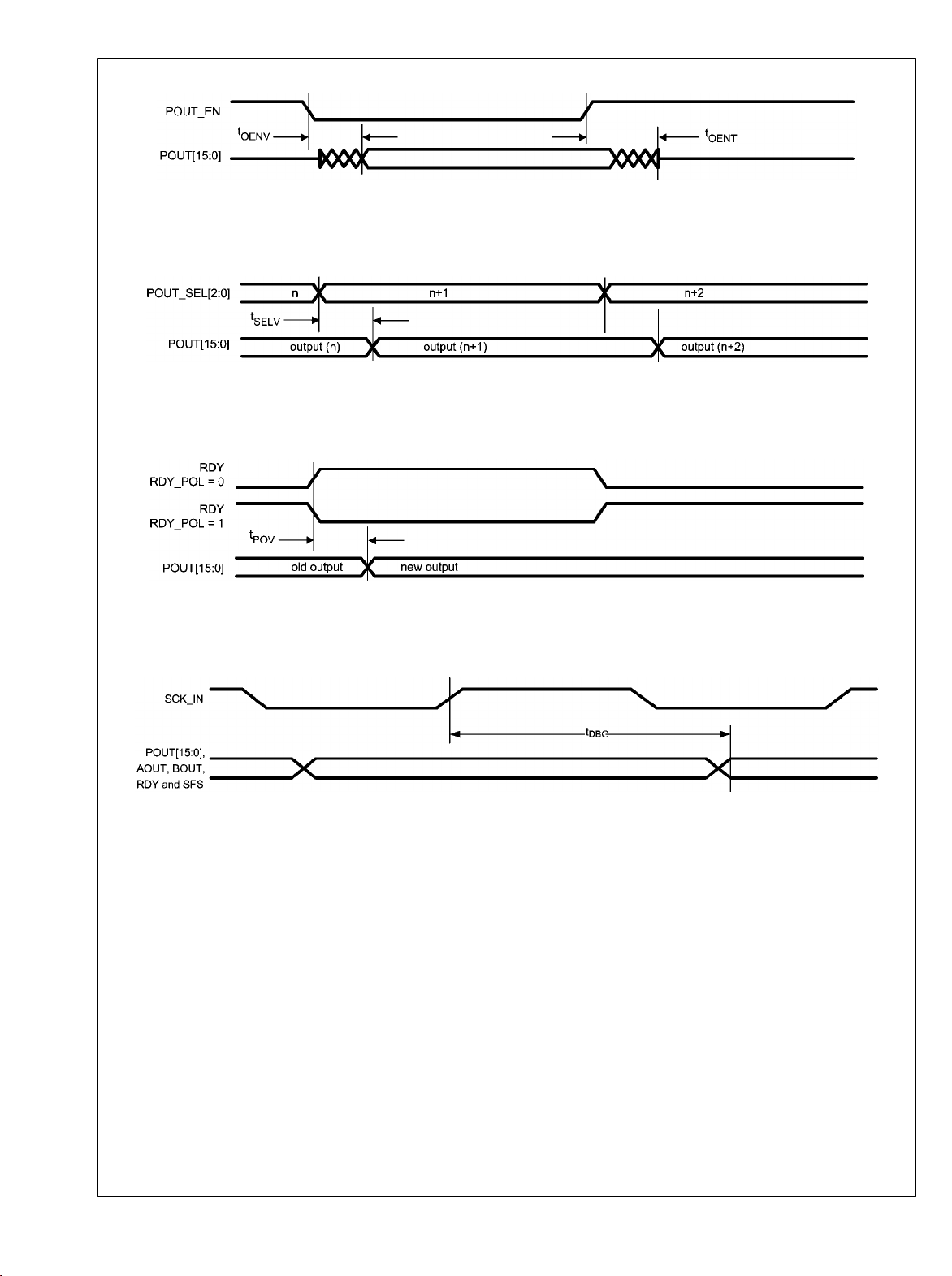
DDC Timing Diagrams
LM97593
30008705
FIGURE 4. LM97593 Master Reset Timing
FIGURE 5. LM97593 Synchronization Input (SI) Timing
FIGURE 6. LM97593 Clock Timing
FIGURE 7. LM97593 DVGA Interface Timing
30008706
30008707
30008708
FIGURE 8. LM97593 Dual Chip Mode Timing
11 www.national.com
30008709
Page 12
LM97593
30008710
FIGURE 9. LM97593 Parallel Output Enable Timing
30008711
FIGURE 10. LM97593 Parallel Output Select Timing
30008712
FIGURE 11. LM97593 Parallel Output Data Ready Timing
FIGURE 12. LM97593 Debug Mode Timing
30008713
www.national.com 12
Page 13

FIGURE 13. LM97593 Serial Port Timing
LM97593
30008714
FIGURE 14. LM97593 JTAG Port Timing
13 www.national.com
30008715
Page 14
LM97593
30008716
FIGURE 15. LM97593 Control I/O Timing
www.national.com 14
Page 15
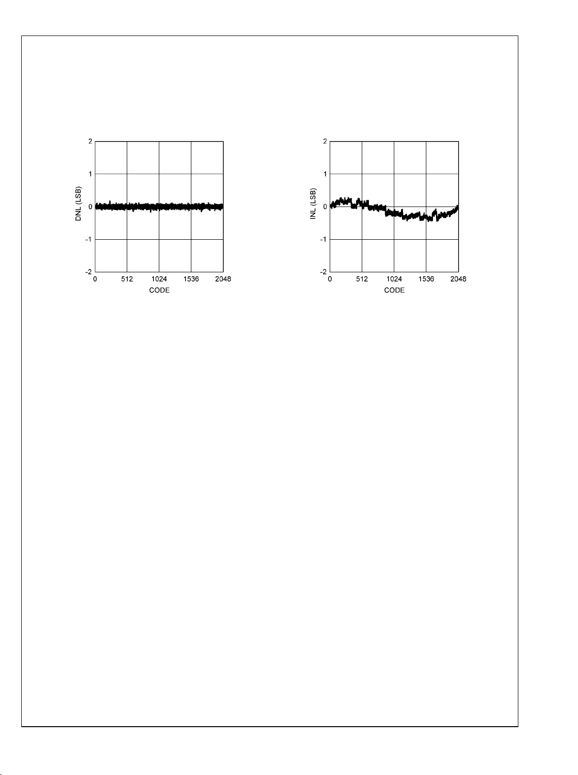
ADC Typical Performance Characteristics DNL, INL
Unless otherwise specified, the following specifications apply for AGND = DGND = D18GND = DRGND = 0V, VA = VD = VDR =
+3.3V, V
Stabilizer On. Boldface limits apply for TJ = T
= +1.8V, PD = 0V, Internal V
D18
= +1.0V, f
REF
MIN
= 65 MHz, fIN = 12 MHz, AIN = 0dBFS, CL = 10 pF/pin, Duty Cycle
CLK
to T
: all other limits TJ = 25°C
MAX
LM97593
DNL
300087100
INL
300087101
15 www.national.com
Page 16

ADC Typical Performance Characteristics
Unless otherwise specified, the following specifications apply for AGND = DGND = D18GND = DRGND = 0V, VA = VD = VDR =
LM97593
+3.3V, V
Stabilizer On. Boldface limits apply for TJ = T
= +1.8V, PD = 0V, Internal V
D18
= +1.0V, f
REF
MIN
= 65 MHz, fIN = 249 MHz, AIN = -9dBFS, CL = 10 pF/pin, Duty Cycle
CLK
to T
: all other limits TJ = 25°C
MAX
SNR, SINAD, SFDR vs. V
Gain Tracking Error vs. V
SUPPLY
SUPPLY
300087102
Distortion vs. V
SUPPLY
300087103
SNR, SINAD, SFDR vs. Temperature
300087104
Distortion vs. Temperature
300087106
www.national.com 16
300087105
Gain Tracking Error vs. Temperature
300087107
Page 17

LM97593
SNR, SINAD, SFDR vs. f
(f
= 52MSPS, AIN = -9dBFS)
CLK
SNR, SINAD, SFDR vs. f
(f
= 52MSPS, AIN = -3dBFS)
CLK
IN
IN
300087110
Distortion vs. f
(f
= 52MSPS, AIN = -9dBFS)
CLK
Distortion vs. f
(f
= 52MSPS, AIN = -3dBFS)
CLK
IN
300087111
IN
SNR, SINAD, SFDR vs. f
(f
= 65MSPS, AIN = -9dBFS)
CLK
IN
300087112
300087114
Distortion vs. f
(f
= 65MSPS, AIN = -9dBFS)
CLK
300087113
IN
300087115
17 www.national.com
Page 18

LM97593
Distortion vs. f
(f
= 65MSPS, AIN = -3dBFS)
CLK
IN
Distortion vs. f
(f
= 65MSPS, AIN = -3dBFS)
CLK
IN
300087116
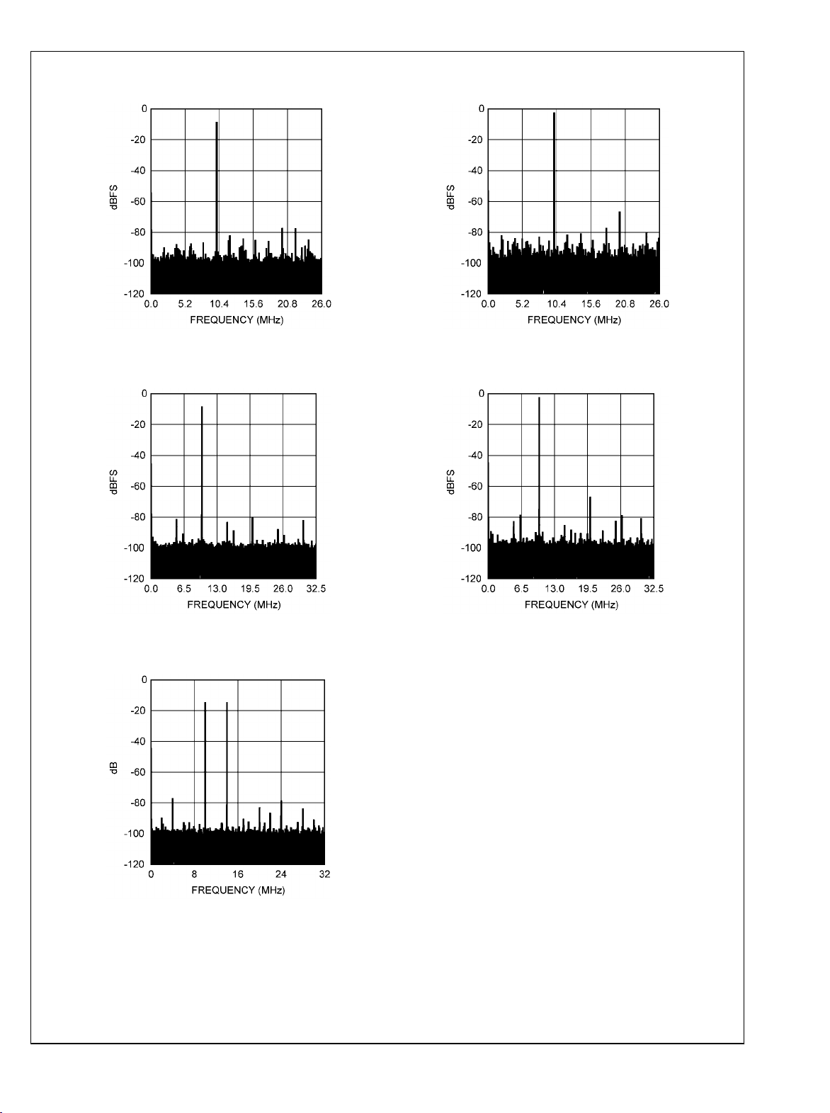
Spectral Response @ 20MHz Input
(f
= 52MSPS, AIN = -9dBFS)
CLK
300087118
Spectral Response @ 20MHz Input
(f
= 65MSPS, AIN = -9dBFS)
CLK
300087117
Spectral Response @ 20MHz Input
(f
= 52MSPS, AIN = -3dBFS)
CLK
300087119
Spectral Response @ 20MHz Input
(f
= 65MSPS, AIN = -3dBFS)
CLK
300087120
www.national.com 18
300087121
Page 19
LM97593
Spectral Response @ 250MHz Input
(f
= 52MSPS, AIN = -9dBFS)
CLK
300087122
Spectral Response @ 250MHz Input
(f
= 65MSPS, AIN = -9dBFS)
CLK
Spectral Response @ 250MHz Input
(f
= 52MSPS, AIN = -3dBFS)
CLK
300087123
Spectral Response @ 250MHz Input
(f
= 65MSPS, AIN = -3dBFS)
CLK
IMD: f
1IN
(f
= 65MSPS, A
CLK
= 246MHz, f
1IN,2IN
= 250MHz
2IN
= -15dBFS)
300087124
300087149
300087125
19 www.national.com
Page 20

CIC Output Typical Performance Characteristics
Unless otherwise specified, the following specifications apply for AGND = DGND = D18GND = DRGND = 0V, VA = VD = VDR =
LM97593
+3.3V, V
Stabilizer On. Boldface limits apply for TJ = T
= +1.8V, PD = 0V, Internal V
D18
= +1.0V, f
REF
MIN
= 65 MHz, fIN = 249 MHz, AIN = -9dBFS, CL = 10 pF/pin, Duty Cycle
CLK
to T
: all other limits TJ = 25°C
MAX
Spectral Response @ 20MHz Input
(f
= 52MSPS, AIN = -9dBFS)
CLK
300087126
Spectral Response @ 20MHz Input
(f
= 65MSPS, AIN = -9dBFS)
CLK
Spectral Response @ 20MHz Input
(f
= 52MSPS, AIN = -3dBFS)
CLK
300087127
Spectral Response @ 20MHz Input
(f
= 65MSPS, AIN = -3dBFS)
CLK
300087128
Spectral Response @ 250MHz Input
(f
= 52MSPS, AIN = -9dBFS)
CLK
300087130
www.national.com 20
300087129
Spectral Response @ 250MHz Input
(f
= 52MSPS, AIN = -3dBFS)
CLK
300087131
Page 21
LM97593
Spectral Response @ 250MHz Input
(f
= 65MSPS, AIN = -9dBFS)
CLK
300087132
Spectral Response @ 250MHz Input
(f
= 65MSPS, AIN = -3dBFS)
CLK
300087133
21 www.national.com
Page 22
DDC Output Typical Performance Characteristics
Unless otherwise specified, the following specifications apply for AGND = DGND = D18GND = DRGND = 0V, VA = VD = VDR =
LM97593
+3.3V, V
pF/pin, Duty Cycle Stabilizer On. Boldface limits apply for TJ = T
= +1.8V, PD = 0V, CIC decimation = 8, Internal V
D18
= +1.0V, f
REF
MIN
to T
= 65 MHz, fIN = 249 MHz, AIN = -9dBFS, CL = 10
CLK
: all other limits TJ = 25°C
MAX
Spectral Response @ 20MHz Input
(f
= 52MSPS, AIN = -9dBFS)
CLK
300087134
Spectral Response @ 20MHz Input
(f
= 65MSPS, AIN = -9dBFS)
CLK
Spectral Response @ 20MHz Input
(f
= 52MSPS, AIN = -3dBFS)
CLK
300087135
Spectral Response @ 20MHz Input
(f
= 65MSPS, AIN = -3dBFS)
CLK
300087136
Spectral Response @ 250MHz Input
(f
= 52MSPS, AIN = -9dBFS)
CLK
300087138
www.national.com 22
300087137
Spectral Response @ 250MHz Input
(f
= 52MSPS, AIN = -3dBFS)
CLK
300087139
Page 23
LM97593
Spectral Response @ 250MHz Input
(f
= 65MSPS, AIN = -9dBFS)
CLK
300087140
Spectral Response @ 250MHz Input
(f
= 65MSPS, AIN = -3dBFS)
CLK
300087141
23 www.national.com
Page 24
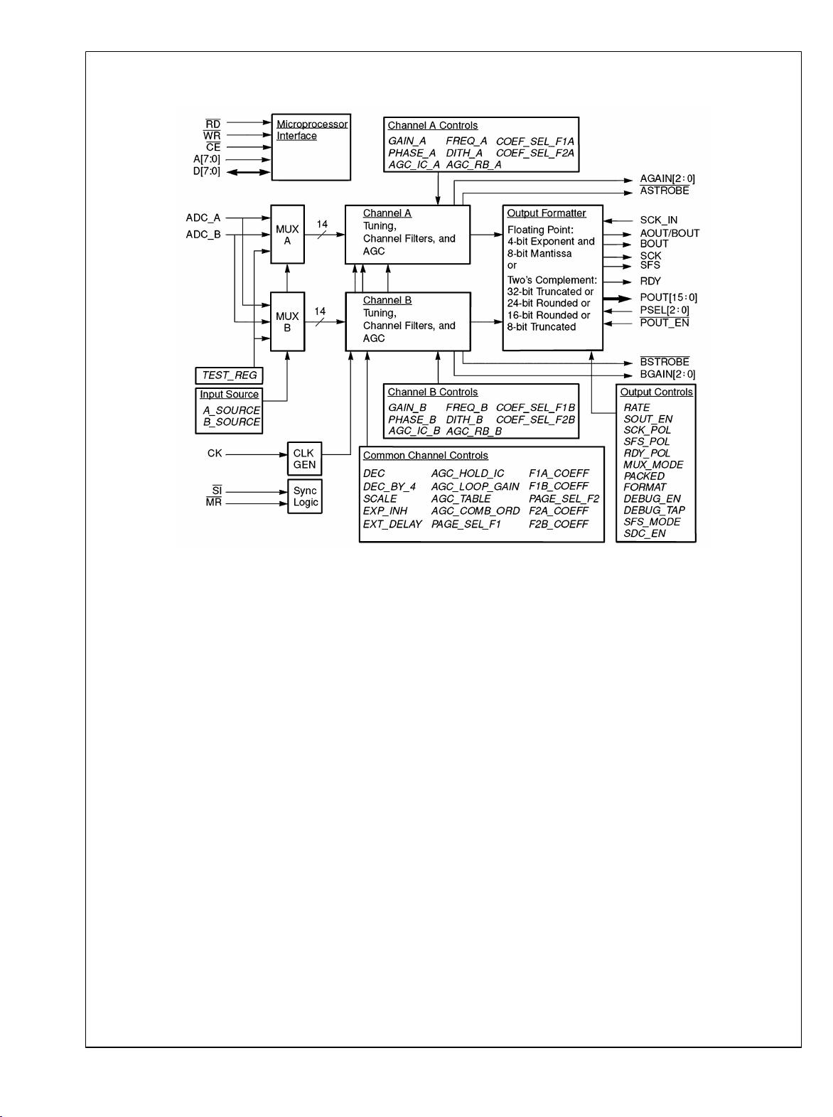
Functional Description
LM97593
FIGURE 16. LM97593 Dual ADC / Digital Tuner / AGC Block Diagram with Control Register Associations
The LM97593 contains two identical 12-bit ADCs driving the
digital down-conversion (DDC) circuitry shown in the block
diagram in Figure 16.
ADC
The ADCs operate off of a +3.3V supply and use a pipeline
architecture with error correction circuitry to help ensure maximum performance. The differential analog input signal is
digitized to 12 bits. The user has the choice of using an internal 1.0 Volt or an external reference. Any external reference
is buffered on-chip to ease the task of driving that pin.
The clock frequency is rated up to 65 MHz. The analog input
for both channels is acquired at the rising edge of the clock.
The digital data for a given sample is delayed by the pipeline
for 7 clock cycles before it reaches the input to the DDC circuit. A logic high on the power down (PD) pin reduces the
converter power consumption to 50 mW. The DDC power can
be further reduced by gating off the clock as described in section 7.0 Power Management.
DDC
Each independent DDC channel down converts the sub-sampled IF to baseband, decimates the signal rate by a programmable factor ranging from 32 to 16384, provides channel
filtering, and outputs quadrature symbols.
A crossbar switch enables either of the two inputs or a test
register to be routed to either DDC channel. Flexible channel
filtering is provided by the two programmable decimating FIR
30008717
filters. The final filter outputs can be converted to a 12-bit
floating point format or standard two’s complement format.
The output data is available at both serial and parallel ports.
The LM97593’s DDC maintains over 100 dB of spurious free
dynamic range and over 100 dB of out-of-band rejection. This
allows considerable latitude in channel filter partitioning between the analog and digital domains.
The frequencies, phase offsets, and phase dither of the two
sine/cosine numerically controlled oscillators (NCOs) can be
independently specified. Two sets of coefficient memories
and a crossbar switch allow shared or independent filter coefficients and bandwidth for each channel. Both channels
share the same decimation ratio and input/output formats.
Each channel has its own AGC circuit for use with narrowband
radio channels where most of the channel filtering precedes
the ADC. The AGC closes the loop around the DVGA, compressing the dynamic range of the signal into the ADC. AGC
gain compensation in the LM97593 removes the DVGA gain
steps at the output. The time alignment of this gain compensation circuit can be adjusted. The AGC can be configured to
operate continuously or set to a fixed gain. The two AGC circuits operate independently but share the same programmed
parameters and control signals.
The chip receives configuration and control information over
a microprocessor-compatible bus consisting of an 8-bit data
I/O port, an 8-bit address port, a chip enable strobe, a read
strobe, and a write strobe. The chip’s control registers (8 bits
each) are memory mapped into the 8-bit address space of the
www.national.com 24
Page 25
LM97593
control port. Page select bits allow access to the overlaid A
and B set of FIR coefficients.
JTAG boundary scan and on-chip diagnostic circuits are provided to simplify system debug and test.
The LM97593 supports 3.3V I/O even though the core logic
voltage is 1.8V. The LM97593 outputs swing to the 3.3V rail
so they can be directly connected to 5V TTL inputs if desired.
ADC Application Information
1.0 ADC OPERATING CONDITIONS
We recommend that the following conditions be observed for
operation:
3.0V ≤ VA ≤ 3.6V
VD = VA = V
V
D18
10 MHz ≤ f
1.0 V internal reference
VCM = 1.5V (from V
1.1 Analog Inputs
There is one reference input pin, V
an internal reference, or to supply an external reference. The
ADC has two analog signal input pairs, VIN A+ and VIN A- for
one converter and VIN B+ and VIN B- for the other converter.
Each pair of pins forms a differential input pair.
1.2 Reference Pins
The ADC is designed to operate with an internal 1.0V reference or an external 1.0V reference, but performs well with
external reference voltages in the range of 0.8V to 1.2V. Lower reference voltages will decrease the signal-to-noise ratio
(SNR) of the ADC. Increasing the reference voltage (and the
input signal swing) beyond 1.2V may degrade THD for a fullscale input, especially at higher input frequencies.
It is important that all grounds associated with the reference
voltage and the analog input signal make connection to the
ground plane at a single, quiet point to minimize the effects of
noise currents in the ground path.
The six Reference Bypass Pins (VRPA, V
V
B and VRNB) are made available for bypass purposes.
COM
All these pins should each be bypassed to ground with a 0.1
µF capacitor. A 10 µF capacitor should be placed between the
VRPA and VRNA pins and between the VRPB and VRNB pins,
as shown in Figure 45. This configuration is necessary to
avoid reference oscillation, which could result in reduced
SFDR and/or SNR.
Smaller capacitor values than those specified will allow faster
recovery from the power down mode, but may result in degraded noise performance. Loading any of these pins other
than V
tion.
The nominal voltages for the reference bypass pins are as
follows:
V
COM
VRP = V
VRN = V
User choice of an on-chip or external reference voltage is
provided. The internal 1.0 Volt reference is in use when the
the V
REF
0.8V to 1.2V is applied to the V
voltage reference. When an external reference is used, the
V
pin should be bypassed to ground with a 0.1 µF capacitor
REF
DR
= 1.8V
≤ 65 MHz
CLK
COM
A and V
A and V
COM
B may result in performance degrada-
COM
B)
COM
, which is used to select
REF
A, VRNA, VRPB,
COM
= 1.5 V
+ V
− V
REF
REF
/ 2
/ 2
COM
COM
pin is connected to VA. If a voltage in the range of
pin, that is used for the
REF
close to the reference input pin. There is no need to bypass
the V
pin when the internal reference is used.
REF
1.3 Signal Inputs
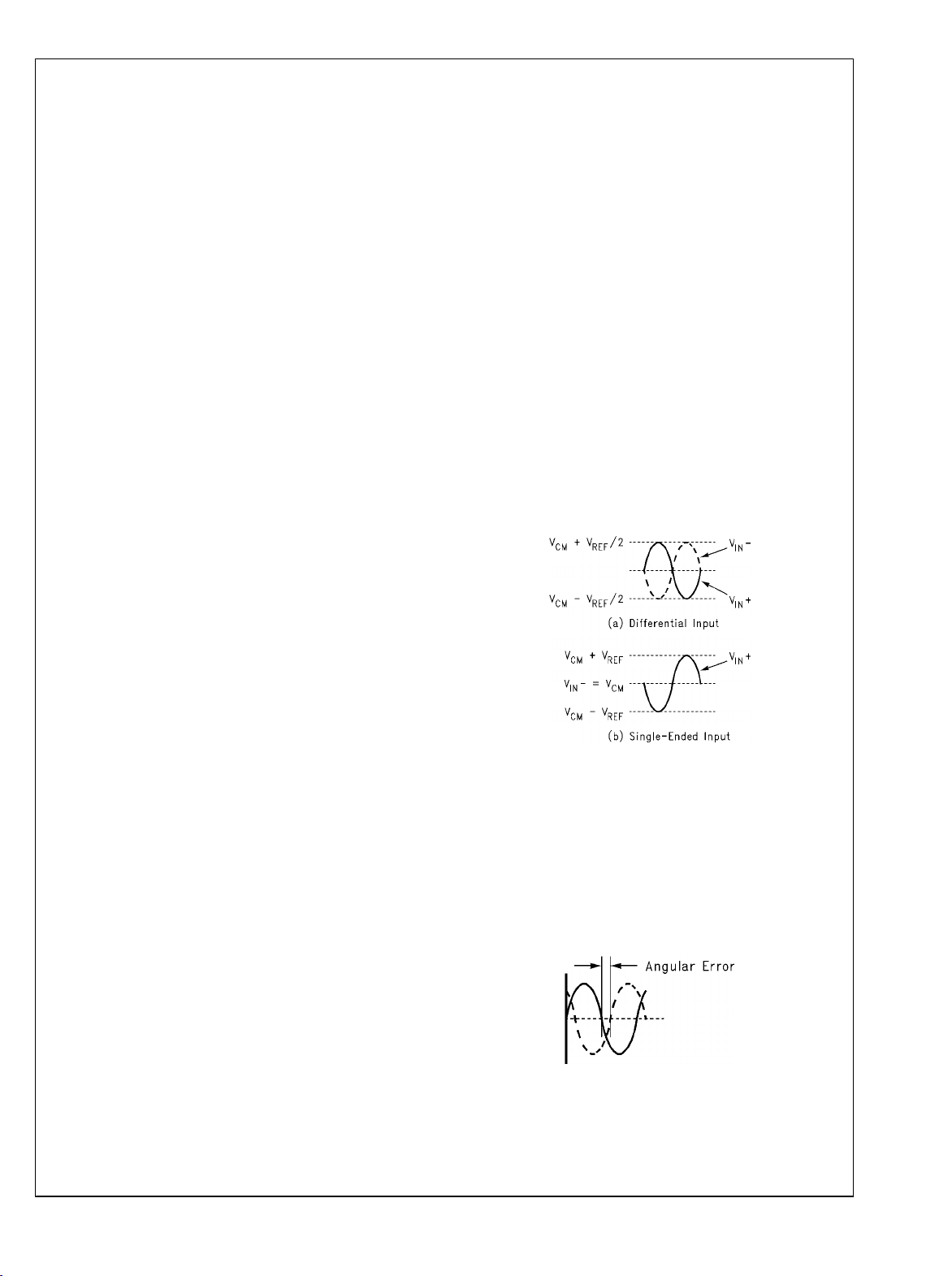
The signal inputs are V
VINB+ and VINB− for the other ADC . The input signal, VIN, is
A+ and VINA− for one ADC and
IN
defined as
VIN A = (VINA+) – (VINA−) (Eq. 1)
for the "A" converter and
VIN B = (VINB+) – (VINB−) (Eq. 2)
for the "B" converter. Figure 17 shows the expected input signal range. Note that the common mode input voltage, VCM,
should be in the range of 1.0V to 2.0V.
The peaks of the individual input signals should never exceed
2.6V.
The ADC performs best with a differential input signal with
each input centered around a common mode voltage, VCM.
The peak-to-peak voltage swing at each analog input pin
should not exceed the value of the reference voltage or the
output data will be clipped.
The two input signals should be exactly 180° out of phase
from each other and of the same amplitude. For single frequency inputs, angular errors result in a reduction of the
effective full scale input. For complex waveforms, however,
angular errors will result in distortion.
30008750
FIGURE 17. Expected Input Signal Range
For single frequency sine waves the full scale error in LSBs
can be described as approximately
EFS = 4096 ( 1 - sin (90° + dev)) (Eq. 3)
Where dev is the angular difference in degrees between the
two signals having a 180° relative phase relationship to each
other (see Figure 18). Drive the analog inputs with a source
impedance less than 100Ω.
30008751
FIGURE 18. Angular Errors Between the Two Input
Signals Will Reduce the Output Level or Cause Distortion
For differential operation, each analog input pin of the differential pair should have a peak-to-peak voltage equal to the
25 www.national.com
Page 26
reference voltage, V
each other and be centered around VCM.
1.3.1 Single-Ended Operation
LM97593
, be 180 degrees out of phase with
REF
Performance with differential input signals is better than with
single-ended signals. For this reason, single-ended operation
is not recommended. However, if single ended-operation is
required and the resulting performance degradation is acceptable, one of the analog inputs should be connected to the
d.c. mid point voltage of the driven input. The peak-to-peak
input signal at the driven input pin should be twice the reference voltage to maximize SNR and SINAD performance
(Figure 17b). For example, set V
and drive VIN+ with a signal range of 0.5V to 2.5V.
to 1.0V, bias VIN− to 1.5V
REF
Because very large input signal swings can degrade distortion
performance, better performance with a single-ended input
can be obtained by reducing the reference voltage when
maintaining a full-range output.
1.3.2 Driving the Analog Inputs
The VIN+ and the VIN− inputs of the ADC consist of an analog
switch followed by a switched-capacitor amplifier. As the internal sampling switch opens and closes, current pulses occur at the analog input pins, resulting in voltage spikes at the
signal input pins. As the driving source attempts to counteract
these voltage spikes, it may add noise to the signal at the ADC
analog input. C1, C2, and C3 as shown in Figure 45 improve
the ADC performance by filtering these voltage spikes. These
components should be placed close to the ADC inputs because the input pins of the ADC are the most sensitive part of
the system and this is the last opportunity to filter that input.
For Nyquist applications the RC pole should be at the ADC
sample rate. The ADC input capacitance in the sample mode
should be considered when setting the RC pole. For wideband undersampling applications, the RC pole should be set
at about 1.5 to 2 times the maximum input frequency to maintain a linear delay response. The values of the RC shown in
Figure 45 are suitable for applications with input frequencies
up to approximately 70MHz.
1.3.3 Input Common Mode Voltage
The input common mode voltage, VCM, should be in the range
of 1.0V to 2.0V and be a value such that the peak excursions
of the analog signal do not go more negative than ground or
more positive than 2.6V. See Section 1.2.
2.0 DIGITAL INPUTS
Digital TTL/CMOS compatible inputs consist of CK, REFSEL/
DCS.
2.1 CLK
The CLK signal controls the timing of the sampling process.
Drive the clock input with a stable, low jitter clock signal in the
range of 10 MHz to 65 MHz. The higher the input frequency,
the more critical it is to have a low jitter clock. The trace carrying the clock signal should be as short as possible and
should not cross any other signal line, analog or digital, not
even at 90°.
The CLK signal also drives an internal state machine. If the
CLK is interrupted, or its frequency too low, the charge on
internal capacitors can dissipate to the point where the accuracy of the output data will degrade. This is what limits the
lowest sample rate.
The clock line should be terminated at its source in the characteristic impedance of that line. Take care to maintain a
constant clock line impedance throughout the length of the
line. Refer to Application Note AN-905 for information on setting characteristic impedance.
It is highly desirable that the the source driving the ADC
CLK pin only drive that pin. However, if that source is used to
drive other things, each driven pin should be a.c. terminated
with a series RC to ground such that the resistor value is equal
to the characteristic impedance of the clock line and the capacitor value is
(Eq. 4)
where tPD is the signal propagation time down the clock line,
"L" is the line length and ZO is the characteristic impedance
of the clock line. This termination should be as close as possible to the ADC clock pin but beyond it as seen from the clock
source. Typical tPD is about 150 ps/inch (60 ps/cm) on FR-4
board material. The units of "L" and tPD should be the same
(inches or centimeters).
The duty cycle of the clock signal can affect the performance
of the A/D Converter. Because achieving a precise duty cycle
is difficult, the LM97593 has a Duty Cycle Stabilizer which can
be enabled using the REFSEL/DCS pin. It is designed to
maintain performance over a clock duty cycle range of 30%
to 70% at 65 MSPS.
2.2 REFSEL/DCS
This pin is used in conjunction with V
reference source and turn the Duty Cycle Stabilizer (DCS) on
(pin 21) to select the
REF
or off.
When REFSEL/DCS is LOW and V
1.0V reference is selected and DCS is On.
is HIGH, the internal
REF
When REFSEL/DCS is HIGH, an external reference voltage
in the range of 0.8V to 1.2V should be applied to the VREF
input. DCS is On.
With REFSEL/DCS pin connected to V
internal 1.0V reference is selected and DCS is Off.
COM
A or V
COM
B, the
When enabled, duty cycle stabilization can compensate for
clock inputs with duty cycles ranging from 30% to 70% and
generate a stable internal clock, improving the performance
of the part.
TABLE 1. V
REFSEL/
, REFSEL/DCS Pin Functions
REF
V
(pin 21) Reference DCS
REF
DCS (pin 8)
Logic Low Logic High Internal 1.0 V ON
Logic High 0.8 to 1.2V External ON
V
V
V
V
COM
COM
COM
COM
A or
B
A or
B
Logic High Internal 1.0V OFF
0.8 to 1.2V External OFF
2.3 PD
The PD pin, when high, holds the ADC in a power-down mode
to conserve power when the converter is not being used. The
output data pins are undefined and the data in the pipeline is
corrupted while in the power down mode.
The Power Down Mode Exit Cycle time is determined by the
value of the components on pins 15, 16, 17, 22, 23 and 24.
These capacitors lose their charge in the Power Down mode
and must be recharged by on-chip circuitry before conversions can be accurate. Smaller capacitor values allow slightly
faster recovery from the power down mode, but can result in
a reduction in SNR, SINAD and ENOB performance.
www.national.com 26
Page 27

LM97593
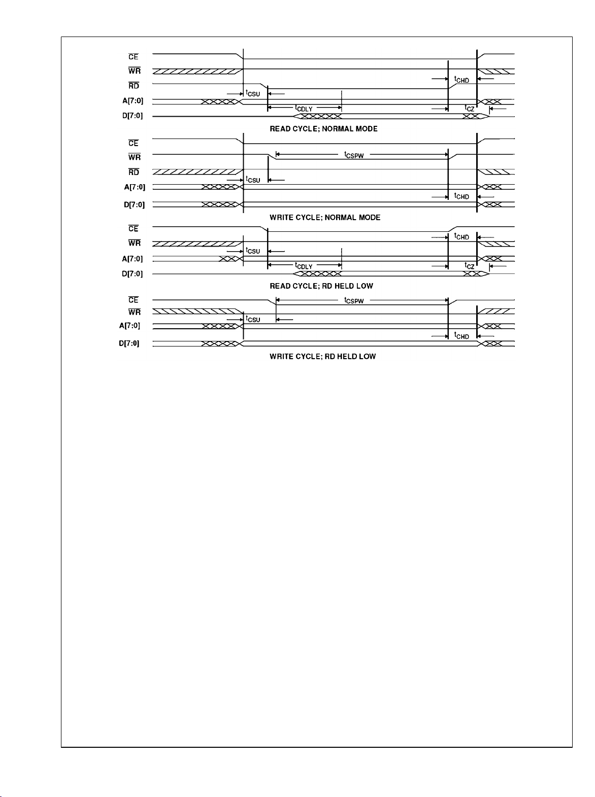
DDC Application Information
3.0 CONTROL INTERFACE
The LM97593 is configured by writing control information into
237 control registers within the chip. The contents of these
control registers and how to use them are described in section
9.1 Control Register Addresses and Defaults. The registers
are written to or read from using the D[7:0], A[7:0], CE
and WR pins. This interface is designed to allow the LM97593
to appear to an external processor as a memory mapped peripheral. See Figure 15 for details.
The control interface is asynchronous with respect to the system clock, CK. This allows the registers to be written or read
at any time. In some cases this might cause an invalid operation since the interface is not internally synchronized. In
order to assure correct operation, SI must be asserted after
the control registers are written.
The D[7:0], A[7:0], WR, RD and CE pins should not be driven
above the positive supply voltage.
3.1 Master Reset
A master reset pin, MR, is provided to initialize the LM97593
to a known condition and should be strobed after power up.
This signal will clear all sample data and all user programmed
data (filter coefficients and AGC settings). All outputs will be
disabled (tri-stated). ASTROBE and BSTROBE will be asserted to initialize the DVGA values. Section 9.1 Control
Register Addresses and Defaults describes the control register default values.
3.2 Synchronizing Multiple LM97593 Chips
A system containing two or more LM97593 chips will need to
be synchronized if coherent operation is desired. To synchronize multiple LM97593 chips, connect all of the sync input pins
together so they can be driven by a common sync strobe.
Synchronization occurs on the first rising edge of CK after
SI
goes high. When SI is asserted all sample data is immediately cleared, the numerically controlled oscillator (NCO)
phase offset is initialized, the NCO dither generators are reset, and the CIC decimation ratio is initialized. Only the configuration data loaded into the microprocessor interface
remains unaffected.
SI may be held low as long as desired after a minimum of 4
CK periods.
, RD
3.3 Input Source
The input crossbar switch allows either VINA, VINB, or a test
register to be routed to the channel A or channel B AGC/ DDC.
The AGC outputs, AGAIN and BGAIN, are not switched. If
VINA and VINB are exchanged the AGC loop will be open and
the AGC will not function properly.
Selecting the test register as the input source allows the AGC
or DDC operation to be verified with a known input. See section 8.0 Test and Diagnostics for further discussion.
4.0 DOWN CONVERTERS
A detailed block diagram of each DDC channel is shown in
Figure 19. Each down converter uses a complex NCO and
mixer to quadrature downconvert a signal to baseband. The
“FLOAT TO FIXED CONVERTER” treats the 15-bit mixer
output as a mantissa and the AGC output, EXP, as a 3-bit
exponent. It performs a bit shift on the data based on the value
of EXP. This bit shifting is used to expand the compressed
dynamic range resulting from the DVGA operation. The DVGA gain is adjusted in 6dB steps which are equivalent to each
digital bit shift.
Digitally compensating for the DVGA gain steps in the
LM97593 causes the DDC output to be linear with respect to
the DVGA input. The AGC operation will be completely transparent at the LM97593 output.
The exponent (EXP) can be forced to its maximum value by
setting the EXP_INH bit. If xin(n) is the DDC input, the signal
after the “FLOAT TO FIXED CONVERTER” is
x3(n) = xin(n)*cos(ωn)*2
for the I component. Changing the ‘cos’ to ‘sin’ in this equation
will provide the Q component.
The “FLOAT TO FIXED CONVERTER” circuit expands the
dynamic range compression performed by the DVGA. Signals
from this point onward extend across the full dynamic range
of the signals applied to the DVGA input. This allows the AGC
to operate continuously through a burst without producing artifacts in the signal due to the settling response of the decimation filters after a 6dB DVGA gain adjustment. For
example, if the DVGA input signal were to increase causing
the ADC output level to cross the AGC threshold level, the
gain of the DVGA would change by -6dB. The 6dB step is
allowed to propagate through the ADC and mixers and is
compensated out just before the filtering. The accuracy of
EXP
(Eq. 5)
FIGURE 19. LM97593 Down Converter, Channel A (Channel B is identical)
27 www.national.com
30008718
Page 28

the compensation is dependent on timing and the accuracy
of the DVGA gain step. The LM97593 allows the timing of the
gain compensation to be adjusted in the EXT_DELAY regis-
LM97593
ter; see the end of section 6.0 AGC for more information. The
AGC requires 21 bits (14-bit internal bus output + 7-bit shift)
to represent the full linear dynamic range of the signal. The
output word must be set to either 24-bit or 32-bit to take advantage of the entire dynamic range available. The LM97593
can also be configured to output a floating point format with
up to 138dB of numerical resolution using only 12 output bits.
The “SHIFT UP” circuit will be discussed in the section 4.2
Four Stage CIC Filter.
A 4-stage cascaded-integrator-comb (CIC) filter and a twostage decimate by 4 or 8 finite impulse response (FIR) filter
are used to lowpass filter and isolate the desired signal. The
CIC filter reduces the sample rate by a programmable factor
ranging from 8 to 2048 (decimation ratio). The CIC outputs
are followed by a gain stage and then followed by a two-stage
decimate by 4 or 8 filter. The gain circuit allows the user to
boost the gain of weak signals by up to 42 dB in 6 dB steps.
It also rounds the signal to 21 bits and saturates at plus or
minus full scale.
The first stage of the two stage filter is a 21-tap, symmetric
decimate by 2 FIR filter (F1) with programmable 16 bit tap
weights. The coefficients of the first 11 taps are downloaded
to the chip as 16 bit words. Since the filter is a symmetric
configuration only the first 11 coefficients must be loaded.
Section 4.4 First Programmable FIR Filter provides a generic
set of coefficients that compensate for the rolloff of the CIC
filter and provide a passband flat to 0.01dB with 70 dB of out
of band rejection. A second coefficient set is provided that has
a narrower output passband and greater out-of-band rejection. The second set of coefficients is ideal for systems such
as GSM where far-image rejection is more important than adjacent channel rejection.
The second stage is a 63 tap decimate by 2 or 4 programmable FIR filter (F2) also with 16 bit tap weights. Filter
coefficients for a flat response from -0.4FS to +0.4FS of the
formance for GSM systems. The user can also design and
download their own final filter to customize the channel’s
spectral response. Typical uses of programmable filter F2 include matched (root-raised cosine) filtering, or filtering to
generate oversampled outputs with greater out of band rejection. The 63 tap symmetrical filter is downloaded into the
chip as 32 words, 16 bits each. Saturation to plus or minus
full scale is performed at the output of F1 and F2 to clip the
signal rather than allow it to roll over.
The LM97593 provides two sets of coefficient memory for
both F1 and F2. These coefficient memories can be independently routed to channel A, channel B, or both channel A and
B with a crossbar switch. The coefficients can be switched on
the fly but some time will be required before valid output data
is available.
4.1 The Numerically Controlled Oscillator
The tuning frequency of each down converter is specified as
a 32 bit word (.02Hz resolution at CK=52MHz) and the phase
offset is specified as a 16 bit word (.005o). These two parameters are applied to the Numerically Controlled Oscillator
(NCO) circuit to generate sine and cosine signals used by the
digital mixer. The NCOs can be synchronized with NCOs on
other chips via the sync pin SI. This allows multiple down
converter outputs to be coherently combined, each with a
unique phase and amplitude.
The tuning frequency is set by loading the FREQ register according to the formula FREQ = 232F/FCK, where F is the
desired tuning frequency and FCK is the chip’s clock rate.
FREQ is a 2’s complement word. The range for F is from
-FCK/2 to +FCK(1-2
-31
)/2.
If a sub-sampled signal is in an even Nyquist zone the sampling process causes the order of the I and Q components to
be reversed. Should this occur simply invert the polarity of the
tuning frequency F.
Complex NCO Output Phase Dither Enabled
Complex NCO Output Phase Dither Disabled
30008719
FIGURE 20. Example of NCO spurs due to phase
truncation
(Before Phase Dithering)
output sample rate with 80dB of out of band rejection are provided in Section 4.5 Second Programmable FIR Filter. A
second set of F2 coefficients is also provided to enhance per-
30008799
FIGURE 21. Example of NCO spurs due to phase
truncation
(After Phase Dithering)
The 2’s complement format represents full-scale negative as
10000000 and full-scale positive as 01111111 for an 8-bit example.
The 16 bit phase offset is set by loading the PHASE register
according to the formula PHASE = 216P/2π, where P is the
desired phase in radians ranging between 0 and 2π. PHASE
www.national.com 28
Page 29

is an unsigned 16-bit number. P ranges from 0 to 2π(1-2
-16
Phase dithering can be enabled to reduce the spurious signals created by the NCO due to phase truncation. This truncation is unavoidable since the frequency resolution is much
finer than the phase resolution. With dither enabled, spurs
due to phase truncation are below -100 dBc for all frequencies
and phase offsets. Each NCO has its own dither source and
the initial state of one is maximally offset with respect to the
other so that they are effectively uncorrelated. The phase
dither sources are on by default. They are independently controlled by the DITH_A and DITH_B bits. The amplitude resolution of the ROM creates a worst-case spur amplitude of
-101dBc rendering amplitude dither unnecessary.
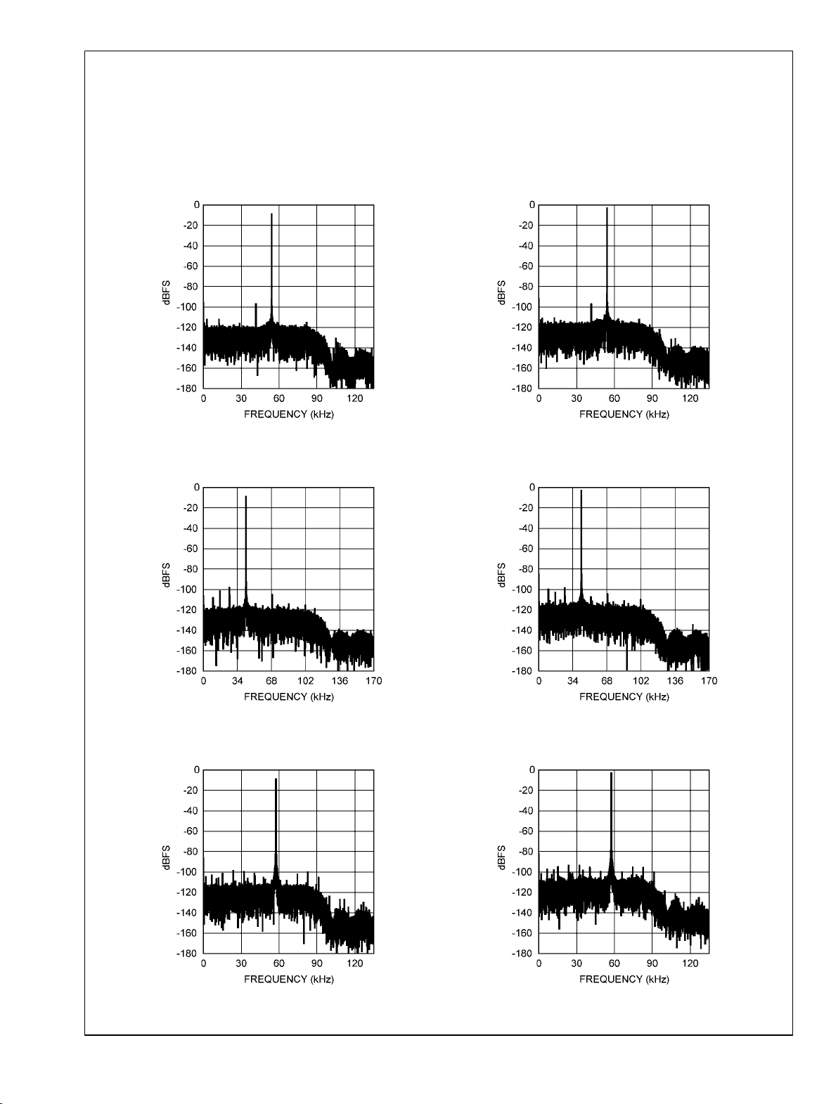
The spectrum plots in Figure 20 and Figure 21show the ef-
fectiveness of phase dither in reducing NCO spurs due to
phase truncation for a worst-case example (just below FS/8).
With dither off, the spur is at -86.4dBFS. With dither on, the
spur is below -125dBFS, disappearing into the noise floor.
This spur is spread into the noise floor which results in an SNR
of -83.6dBFS. The channel filter’s processing gain will further
improve the SNR.
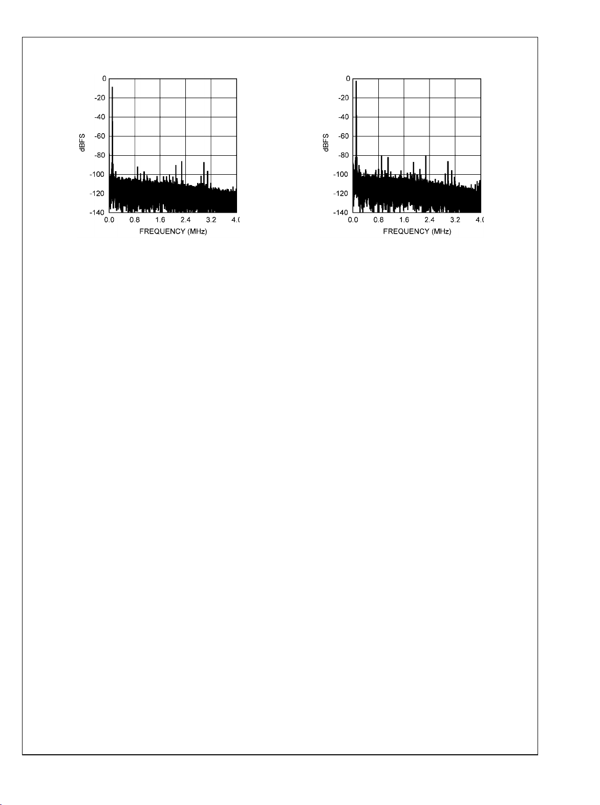
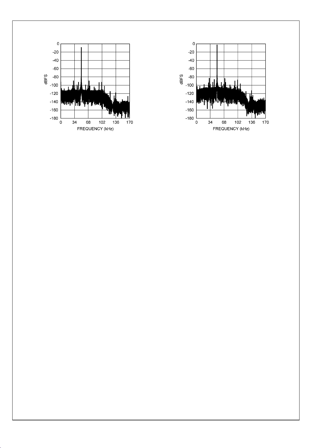
Figure 22 shows the spur levels as the tuning frequency is
scanned over a narrow portion of the frequency range. The
spurs are again a result of phase quantization but their locations move about as the frequency scan progresses. As before, the peak spur level drops when dithering is enabled.
When dither is enabled and the fundamental frequency is exactly at FS/8, the worst-case spur due to amplitude quantization can be observed at -101dBc in Figure 23.
LM97593
).
Complex NCO Output Phase Dither Disabled
30008720
FIGURE 22. NCO Spurs due to Phase Quantization
Complex NCO Output Phase Dither Enabled
4.2 Four Stage CIC Filter
The mixer outputs are decimated by a factor of N in a four
stage CIC filter. N is programmable to any integer between 8
and 2048. Decimation is programmed in the DEC register
where DEC = N - 1. The programmable decimation allows the
chip’s usable output bandwidth to range from about ±1.27kHz
to ±650kHz when the input data rate (which is equal to the
chip’s clock rate, FCK) is 52 MHz. For the maximum sample
rate of 65MHz, the LM97593’s output bandwidth will range
from about ±1.58kHz to ±812kHz. A block diagram of the CIC
filter is shown in Figure 24.
The CIC filter is primarily used to decimate the high-rate incoming data while providing a rough lowpass characteristic.
The lowpass filter will have a sin(x)/x response (similar to the
AGC’s CIC shown in Figure 39) where the first null is at FS/N.
30008721
FIGURE 23. Worst Case Amplitude Spur, NCO at FS/8
The CIC filter has a gain equal to N4 (filter decimation^4)
which must be compensated for in the “SHIFT UP” circuit
shown in Figure 24 as well as Figure 19. This circuit has a
gain equal to 2
(SCALE-44)
, where SCALE ranges from 0 to 40.
This circuit divides the input signal by 244 providing
FIGURE 24. Four-stage decimate by N CIC filter
maximum headroom through the CIC filter. For optimal noise
performance the SCALE value is set to increase this level until
30008722
the CIC filter is just below the point of distortion. A value is
normally calculated and loaded for SCALE such that
29 www.national.com
Page 30

GAIN
only be unity for power-of-two decimation values. In other
cases the gain will be somewhat less than unity.
LM97593
SHIFTUP
*GAIN
≤ 1. The actual gain of the CIC filter will
CIC
4.3 Channel Gain
The gain of each channel can be boosted up to 42 dB by
shifting the output of the CIC filter left by 0 to 7 bits prior to
rounding it to 21 bits. For channel A, the gain of this stage is:
GAIN = 2
GAIN_A
, where GAIN_A ranges from 0 to 7. Overflow
due to the GAIN circuit is saturated (clipped) at plus or minus
full scale. Each channel can be given its own GAIN setting.
4.4 First Programmable FIR Filter (F1)
The CIC/GAIN outputs are followed by two stages of filtering.
The first stage is a 21 tap decimate-by-2 symmetric FIR filter
with programmable coefficients. Typically, this filter compensates for a slight droop induced by the CIC filter while removing undesired alias images above Nyquist. In addition, it often
provides stopband assistance to F2 when deep stop bands
are required. The filter coefficients are 16-bit 2’s complement
numbers. Unity gain will be achieved through the filter if the
sum of the 21 coefficients is equal to 216. If the sum is not
216, then F1 will introduce a gain equal to (sum of coefficients)/
216. The 21 coefficients are identified as coefficients h1(n), n
= 0, ..., 20 where h1(10) is the center tap. The coefficients are
symmetric, so only the first 11 are loaded into the chip.
Two example sets of coefficients are provided here. The first
set of coefficients, referred to as the standard set (STD), compensates for the droop of the CIC filter providing a passband
which is flat (0.01 dB ripple) over 95% of the final output
bandwidth with 70dB of out-of-band rejection (see Figure
25). The filter has a gain of 0.999 and is symmetric with the
following 11 unique taps (1|21, 2|20, ..., 10|12, 11):
29, -85, -308, -56, 1068, 1405, -2056, -6009,
1303, 21121, 32703
30008724
FIGURE 26. F1 GSM frequency response
4.5 Second Programmable FIR Filter (F2)
The second stage decimate by two or four filter also uses externally downloaded filter coefficients. F2 determines the final
channel filter response. The filter coefficients are 16-bit 2’s
complement numbers. Unity gain will be achieved through the
filter if the sum of the 63 coefficients is equal to 216. If the sum
is not 216, then the F2 will introduce a gain equal to (sum of
coefficients)/216.
The 63 coefficients are identified as h2(n), n = 0, ..., 62 where
h2(31) is the center tap. The coefficients are symmetric, so
only the first 32 are loaded into the chip. An example filter
(STD F2 coefficients, see Figure 27) with 80dB out-of-band
rejection, gain of 1.00, and 0.03 dB peak to peak passband
ripple is created by this set of 32 unique coefficients:
-14, -20, 19, 73, 43, -70, -82, 84, 171, -49, -269,
-34, 374, 192, -449,
-430, 460,751, -357, -1144, 81, 1581, 443, -2026,
-1337, 2437, 2886,
-2770, -6127, 2987, 20544, 29647
A second set of F2 coefficients (GSM set, see Figure 28) suit-
able for meeting the stringent wideband GSM requirements
with a gain of 0.999 are:
-536, -986, 42, 962, 869, 225, 141, 93, -280,
-708, -774, -579, -384,
-79, 536, 1056, 1152, 1067, 789, 32, -935, -1668,
-2104, -2137, -1444,
71, 2130, 4450, 6884, 9053, 10413, 10832
The filter coefficients of both filters can be used to tailor the
spectral response to the user’s needs. For example, the first
can be loaded with the standard set to provide a flat
30008723
FIGURE 25. F1 STD frequency response
The second set of coefficients (GSM set) are intended for applications that need deeper stop bands or need oversampled
outputs. These requirements are common in cellular systems
where out of band rejection requirements can exceed 100dB
(see Figure 26). They are useful for wideband radio architectures where the channelization is done after the ADC. These
filter coefficients introduce a gain of 0.984 and are:
-49, -340, -1008, -1617, -1269, 425, 3027, 6030,
9115, 11620, 12606
www.national.com 30
Page 31

LM97593
30008725
FIGURE 27. F2 STD frequency response
30008726
FIGURE 28. F2 GSM frequency response
response through to the second filter. The latter can then be
programmed as a Nyquist (typically a root-raised-cosine) filter
for matched filtering of digital data.
The complete channel filter response for standard coefficients
is shown in Figure 29. Passband flatness is shown in Figure
30. The complete filter response for GSM coefficients is
shown in Figure 31. GSM Passband flatness is shown in Fig-
ure 32.
The mask shown in Figure 31 is derived from the ETSI GSM
5.05 specifications for a normal Basestation Transceiver
(BTS). For interferers, 9dB was added to the carrier to interference (C/I) ratios. For blockers, 9dB was added to the
difference between the blocker level and 3dB above the reference sensitivity level.
30008727
FIGURE 29. CIC, F1, & F2 STD frequency response
30008728
FIGURE 30. CIC, F1, & F2 STD Passband Flatness
4.6 Channel Bandwidth vs. Sample Rate
When the LM97593 is used for GSM systems, a bandwidth of
about 200kHz is desired. With a sample rate of 52MHz, the
total decimation of 192 provides the desired 270.833kHz output sample rate. This output sample rate in combination with
the FIR filter coefficients create the desired channel bandwidth. If the sample rate is increased to 65MHz, the decimation must also be increased to 65MHz/270.833kHz or 240.
This new decimation rate will maintain the same output
30008729
FIGURE 31. CIC, F1, & F2 GSM frequency response
bandwidth. The output bandwidth may only be changed in relation to the output sample rate by creating a new set of FIR
filter coefficients. As the filter bandwidth
31 www.national.com
Page 32

wave inputs the 1/2 should be set to 1 to prevent signal distortion.
LM97593
FIGURE 32. CIC, F1, & F2 GSM Passband Flatness
decreases relative to the output sample rate, the CIC droop
compensation performed by F1 may no longer be required.
4.7 Overall Channel Gain
The overall gain of the chip is a function of the amount of
decimation (N), the settings of the “SHIFT UP” circuit
(SCALE), the GAIN setting, the sum of the F1 coefficients,
and the sum of the F2 coefficients. The overall gain is shown
below in Equation 2.
30008730
4.8 Data Latency and Group Delay
The LM97593 latency calculation assumes that the FIR filter
latency will be equal to the time required for data to propagate
through one half of the taps. The CIC filter provides 4N equivalent taps where N is the CIC decimation ratio. F1 and F2
provide 21 and 63 taps respectively. When these filters are
reflected back to the input rate, the effective taps are increased by decimation. This results in a total of 151N taps.
The total latency is found by dividing the number of taps by 2
and adding pipeline delays. When the F2 decimation is 2 the
latency is 80N. When the F2 decimation is 4 the latency is
82N. The LM97593 filters are linear phase filters so the group
delay remains constant.
5.0 OUTPUT MODES
After processing by the DDC, the data is then formatted for
output.
All output data is two’s complement. The serial outputs
power up in a tri-state condition and must be enabled
when the chip is configured. Parallel outputs are enabled
by the POUT_EN pin.
Output formats include truncation to 8 or 32 bits, rounding to
16 or 24 bits, and a 12-bit floating point format (4-bit exponent,
8-bit mantissa, 138dB numeric range). This function is performed in the OUTPUT CIRCUIT shown in Figure 33.
(Eq. 6)
Where:
(Eq. 7)
and:
(Eq. 8)
It is assumed that the DDC output words are treated as fractional 2’s complement words. The numerators of GF1 and
GF2 equal the sums of the impulse response coefficients of
F1 and F2, respectively. For the STD and GSM sets, GF1 and
GF2 are nearly equal to unity. Observe that the AGAIN term
in (Eq. 6) is cancelled by the DVGA operation so that the entire gain of the DRCS is independent of the DVGA setting
when EXP_INH=0. The 1/2 appearing in (Eq. 6) is the result
of the 6dB conversion loss in the mixer. For full-scale square
30008731
FIGURE 33. LM97593 output circuit
The channel outputs are accessible through serial output pins
and a 16-bit parallel output port. The RDY pin is provided to
notify the user that a new output sample period (OSP) has
begun. OSP refers to the interval between output samples at
the decimated output rate. For example, if the input rate (and
clock rate) is 52 MHz and the overall decimation factor is 192
(N=48, F2 decimation=2) the OSP will be 3.69 microseconds
which corresponds to an output sample
www.national.com 32
Page 33
LM97593
FIGURE 34. Serial output formats. Refer to Figure 13 for detailed timing information
rate of 270.833kHz. An OSP starts when a sample is ready
and stops when the next one is ready.
5.1 Serial Outputs
The LM97593 provides a serial clock (SCK), a frame strobe
(SFS) and two data lines (AOUT and BOUT) to output serial
data. The MUX_MODE control register specifies whether the
two channel outputs are transmitted on two separate serial
pins, or multiplexed onto one pin in a time division multiplexed
(TDM) format. Separate output pins are not provided for the I
and Q halves of complex data. The I and Q outputs are always
multiplexed onto the same serial pin. The I-component is output first, followed by the Q-component. By setting the
PACKED mode bit to ‘1’ a complex pair may be treated as a
single double-wide word. The RDY signal is used to identify
the first word of a complex pair of the TDM formatted output
when the SFS_MODE bit is set to ‘0’. Setting SFS_MODE to
‘1’ causes the LM97593 to output a single SFS pulse for each
30008732
output period. This SFS pulse will be coincident with RDY and
only a single SCK period wide. The TDM modes are summarized in Table 2.
TABLE 2. TDM Modes
SFS_MODE MUX_MODE
0
0
1
1
0
1
SERIAL OUTPUTS
AOUT BOUT
OUT
A
OUTA, OUT
OUT
OUTA, OUT
B
A
B
OUT
LOW
OUT
LOW
B
B
The serial outputs use the format shown in Figure 34. Figure
34(a) shows the standard output mode (the PACKED mode
bit is low). The chip clocks the frame and data out of the chip
33 www.national.com
Page 34

LM97593
30008733
FIGURE 35. Serial Daisy-Chain Mode
on the rising edge of SCK (or falling edge if the SCK_POL bit
in the input control register is set high). Data should be captured on the falling edge of SCK (rising if SCK_POL=1). The
chip sends the I data first by setting SFS high (or low if
SFS_POL in the input control register is set high) for one clock
cycle, and then transmitting the data, MSB first, on as many
SCK cycles as are necessary. Without a pause, the Q data is
transferred next as shown in Figure 34(a). If the PACKED
control bit is high, then the I and Q components are sent as a
double length word with only one SFS strobe as shown in
Figure 34(b). If both channels are multiplexed out the same
serial pin, then the subsequent I/Q channel words will be
transmitted immediately following the first I/Q pair as shown
in Figure 34(c). Figure 34(c) also shows how SFS_MODE=1
allows the SFS signal to be used to identify the A and B channels in the TDM serial transmission. The serial output rate is
programmed by the RATE register to CK divided by 1, 2, 4,
8, 16, or 32. The serial interface will not work properly if the
programmed rate of SCK is insufficient to clock out all the bits
in one OSP.
5.2 Serial Port Daisy-Chain Mode
Two LM97593s can be connected in series so that a single
DSP serial port can receive four DDC output channels. This
mode is enabled by setting the SDC_EN bit to ‘1’ on the serial
daisy-chan (SDC) master. The SDC master is the LM97593
which is connected to the DSP while the SDC slave’s serial
output drives the master. The SDC master’s RATE register
must be set so that its SCK rate is twice that of the SDC slave,
the SDC master must have MUX_MODE=1, the SDC slave
must have MUX_MODE=0 and PACKED=1, and both chips
must come out of a MR or SI event within four CK periods of
each other. In this configuration, the master’s serial output
data is shifted out to the DSP and then the slave’s serial data
is shifted out. All the serial output data will be muxed onto the
master’s AOUT pin as shown in Figure 35.
5.3 Serial Port Output Number Formats
Several numeric formats are selectable using the FORMAT
control register. The I/Q samples can be rounded to 16 or 24
bits, or truncated to 8 bits. The packed mode works as described above for these fixed point formats. A floating point
format with 138dB of dynamic range in 12 bits is also provided. The mantissa (m) is 8 bits and the exponent (e) is 4 bits.
The MSB of each segment is transmitted first. When the
packed mode is selected, the I/Q samples are packed re-
gardless of the state of MUX_MODE, and the data is sent as
mI/eI/eQ/ mQ which allows the two exponents to form an 8bit word. This is shown in Figure 34(d). For all formats, once
the defined length of the word is complete, SCK stops toggling.
5.4 Parallel Outputs
Output data from the channels can also be taken from a 16bit parallel port. A 3-bit word applied to the POUT_SEL[2:0]
pins determines which 16-bit segment is multiplexed to the
parallel port. Table 3 defines this mapping. To allow for bussing of multiple chips, the parallel port is tri-stated unless
POUT_EN is low. The RDY signal indicates the start of an
OSP and that new data is ready at the parallel output. The
user has one OSP to cycle through whichever registers are
needed. The RATE register must be set so that each OSP is
at least 5 SCK periods.
5.4.1 Parallel Port Output Numeric Formats
The I/Q samples can be rounded to 16 or 24 bits or the full 32
bit word can be read. By setting the word size to 32 bits it is
possible to read out the top 16-bits and only observe the top
8 bits if desired. Additionally, the output samples can be formatted as floating point numbers with an 8-bit mantissa and
a 4 bit exponent. For the fixed-point formats, the valid bits are
justified into the MSBs of the registers of Table 3 and
TABLE 3. Register Selection for Parallel Output
Floating Point
Register
Contents
POUT_SEL
Normal Register
Contents
0 IA upper 16-bits 0000/eIA/mIA
1 IA lower 16-bits 0x0000
2 QA upper 16-bits 0000/eQA/mQA
3 QA lower 16-bits 0x0000
4 IB upper 16-bits 0000/eIB/mIB
5 B lower 16-bits 0x0000
6 QB upper 16-bits 0000/eQB/mQB
7 QB lower 16-bits 0x0000
all other bits are set to zero. For the floating point format, the
valid bits are placed in the upper 16-bits of the appropriate
channel register using the format 0000/eI/mI for the I samples.
www.national.com 34
Page 35
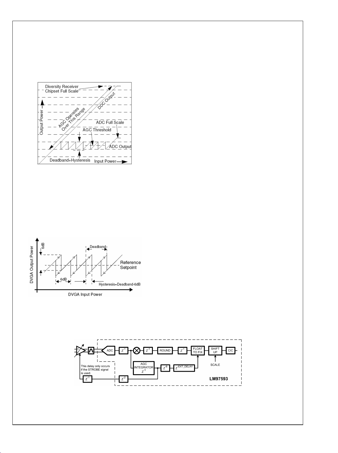
LM97593
6.0 AGC
The LM97593 AGC processor monitors the output level of the
ADC and servos it to the desired setpoint. The ADC input is
controlled by the DVGA to maintain the proper setpoint level.
DVGA operation results in a compression of the signal
through the ADC. The DVGA signal compression is reversed
in the LM97593 to provide > 120dB of linear dynamic range.
This is illustrated in Figure 36.
30008734
FIGURE 36. Output Gain Scaling vs. Input Signal
In order to use the AGC, the DRCS Control Panel software
may be used to calculate the programmable parameters. To
generate these parameters, only the desired setpoint, deadband+ hysteresis, and loop time constant need to be supplied.
All subsequent calculations are performed by the software.
Complete details of the AGC operation are provided in an appendix.
30008735
FIGURE 37. AGC Setup
AGC setpoint and deadband are illustrated in Figure 37. The
loop time constant is a measure of how fast the loop will track
a changing signal. Values down to approximately 1.0 microsecond will be stable with the second order LC noise filter.
Since the DVGA operates with 6dB steps the deadband
should always be greater than 6dB to prevent oscillation. An
increased deadband value will reduce the amount of AGC
operation. A decreased deadband value will increase the
amount of AGC operation but will hold the ADC output closer
to the setpoint. The threshold should be set so that transients
do not cause sustained overrange at the ADC inputs. The
threshold setting can also be used to set the ADC input near
its optimal performance level.
The AGC will free run when AGC_HOLD_IC is set to ‘0’. It
may be set to a fixed gain by setting AGC_HOLD_IC to ‘1’
after programming the desired gain in the AGC_IC_A and
AGC_IC_B registers. Allowing the AGC to free run should be
appropriate for most applications.
Programming the AGC_COMB_ORD register allows the AGC
power detector bandwidth to be reduced if desired. This will
tend to improve the power detector’s ability to reject the signal
carrier frequency and reduce overall AGC activity. Figure 39
shows the power detector response.
The analog gain change from the DVGA must be compensated by the "Float To Fixed" converter after the appropriate
delay. This delay can be adjusted by the EXT_DELAY register
value to make sure the analog gain change is properly compensated in the digital domain.
Figure 38 shows the internal clock latency paths related to the
DVGA and "Float To Fixed" timing conpensation. In this diagram registers are represented by z-N where N is the sample
delay in ADC clock periods. Following the path from the output
of the AGC integrator through the DVGA, bandpass filter,
ADC and internal register delays adds up to 6 clocks prior to
the "Float To Fixed" converter excluding the bandpass filter
and ADC. Following the path from the AGC integrator to the
"Float To Fixed" is also 6 clocks when EXT_DELAY = 0. The
value programmed in EXT_DELAY should be set to the
pipeline latency of the ADC plus the latency of the bandpass
filter (typically one clock). If ASTROBE and BSTROBE are not
used then subtract one from the resulting total latency.
The LM97593 includes an integrated ADC with a pipeline latency of 7 clocks. Adding one additional clock period for the
bandpass filter requires EXT_DELAY = 7 when the DVGA
ASTROBE and BSTROBE signals are used, otherwise, program EXT_DELAY = 6. In most cases ASTROBE and
BSTROBE signals are not used so EXT_DELAY is typically
set to 6.
More accurate time alignment may improve the equalizer /
demodulator performance for EDGE modulated signals and
other signals with a large AM component.
FIGURE 38. Function controlled by EXT_DELAY register
35 www.national.com
30008758
Page 36
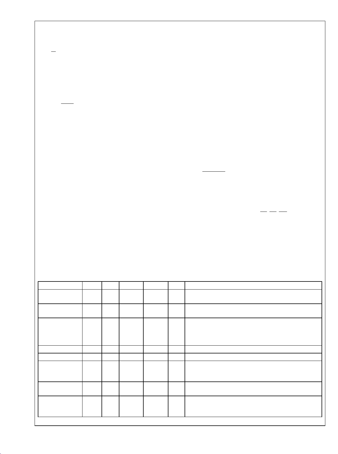
7.0 POWER MANAGEMENT
The LM97593 can be placed in a low power (static) state by
stopping the input clock and setting the PD pin high. To pre-
LM97593
vent this from placing the LM97593 into unexpected states,
pin of the LM97593 should be asserted prior to dis-
the SI
abling the input clock and held asserted until the input clock
has returned to a stable condition.
8.0 TESTABILITY
8.1 JTAG Boundary Scan
The LM97593 supports IEEE 1149.1 compliant JTAG Boundary Scan for the I/O's. The following pins are used:
TRST (test reset)
TMS (test mode select)
TDI (test data in)
TDO (test data out)
TCK (test clock)
The following JTAG instructions are supported:
Instruction Description
BYPASS Connects TDI directly to TDO
EXTEST Enables the test access port
controller to drive the outputs
IDCODE Connects the 32-bit ID register to
TDO
SAMPLE/PRELOAD Allows the test access port to
sample the device inputs and
preload test output data
HIGHZ Tri-states the outputs
The JTAG Boundary Scan can be used to verify printed circuit
board continuity at the system level.
8.2 Test Register
The user is able to program a value into TEST_REG and
substitute this for the normal channel inputs from the AIN/
BIN pins by selecting it with the crossbar. With the NCO frequency set to zero this allows the DDCs and the output
interface of the chip to be verified. Also, the AGC loop can be
opened by setting AGC_HOLD_IC high and setting the gain
of the DVGA by programming the appropriate value into the
AGC_IC_A/B register.
8.3 Debug Access Port
Real-time access to the following signals is provided by configuring the control interface debug register:
•
NCO sine and cosine outputs
•
data after round following mixers
•
data before F1 and F2
•
data after CIC filter within the AGC
The access points are multiplexed to a 20-bit parallel output
port which is created from signal pins POUT[15:0], AOUT,
BOUT, SFS, and RDY according to the table below:
Normal Mode Pin Debug Mode Pin
POUT[15:0] DEBUG[19:4]
RDY DEBUG[3]
SFS DEBUG[2]
AOUT DEBUG[1]
BOUT DEBUG[0]
SCK will be set to the proper strobe rate for each debug tap
point. POUT_EN and PSEL[2:0] have no effect in Debug
Mode. The outputs are turned on when the Debug Mode bit
is set. Normal serial outputs are also disabled.
9.0 CONTROL REGISTERS
The chip is configured and controlled through the use of 8-bit
control registers. These registers are accessed for reading or
writing using the control bus pins (CE, RD, WR, A[7:0], and D
[7:0]) described in section 3.0 Control Interface.
The two sets of FIR coefficients are overlaid at the same
memory address. Use the PAGE_SEL registers to access
the second set of coefficients.
The register names and descriptions are listed below in section 9.1 Control Register Addresses and Defaults. A quick
reference table is provided in the Condensed LM97593 Ad-
dress Map.
9.1 Control Register Addresses and Defaults
a
Register Name Width Type
DEC 11b R/W 7
DEC_BY_4 1b R/W 0 1 4
Default
Addr Bit Description
0(LSBs)
1(MSBs)
7:0
CIC decimation control. N=DEC+1. Valid range is from 7 to
2:0
2047. Format is an unsigned integer. This affects both channels.
Controls the decimation factor in F2. 0=Decimate by 2.
1=Decimate by 4. This affects both channels.
CIC SCALE parameter. Format is an unsigned integer
SCALE 6b R/W 0 2 5:0
representing the number of left bit shifts to perform on the data
prior to the CIC filter. Valid range is from 0 to 40. This affects
both channels.
GAIN_A 3b R/W 0 3 2:0 Value of left bit shift prior to F1 for channel A.
GAIN_B 3b R/W 0 4 2:0 Value of left bit shift prior to F1 for channel B.
Determines rate of serial output clock. The output rate is FCK/
RATE 1B R/W 1 5 7:0
(RATE+1). Unsigned integer values of 0, 1, 3, 7, 15, and 31 are
allowed.
SOUT_EN 1b R/W 0 6 0
Enables the serial output pins AOUT, BOUT, SCK, and SFS.
0=Tristate. 1=Enabled.
Determines polarity of the SCK output. 0=AOUT, BOUT, and
SCK_POL 1b R/W 0 6 1
SFS change on the rising edge of SCK (capture on falling edge).
1=They change on the falling edge of SCK.
www.national.com 36
Page 37
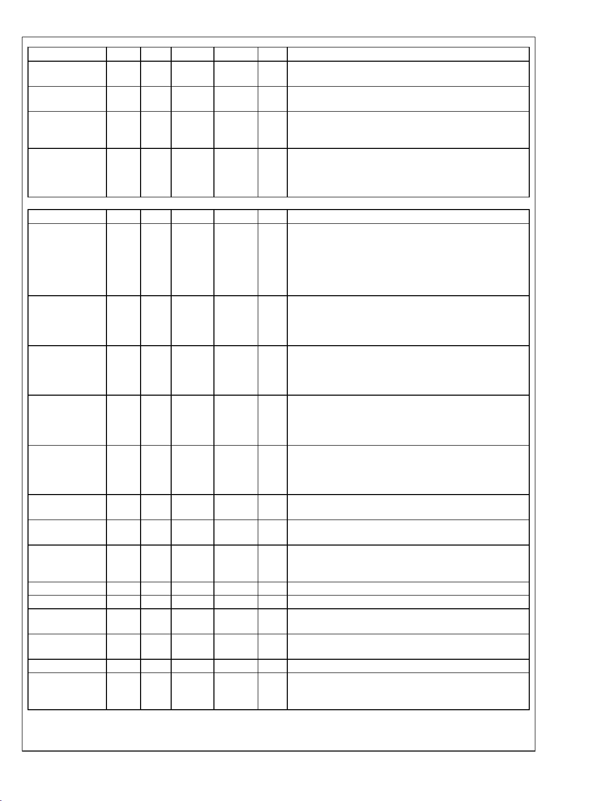
a
Register Name Width Type
SFS_POL 1b R/W 0 6 2
RDY_POL 1b R/W 0 6 3
Default
Addr Bit Description
Determines polarity of the SFS output. 0=Active High. 1=Active
Low.
Determines polarity of the RDY output. 0=Active High. 1=Active
Low.
Determines the mode of the serial outputs. 0=Each channel is
MUX_MODE 1b R/W 0 6 4
output on its respective pin, 1=Both channels are multiplexed
and output on AOUT. See also .
Controls when SFS goes active. 0=SFS pulses prior to the start
PACKED 1b R/W 0 6 5
of the I and the Q words. 1=SFS pulses only once prior to the
start of each I/Q sample pair (i.e. the pair is treated as a doublesized word) The I word precedes the Q word. See .
a
Register Name Width Type
Default
Addr Bit Description
Determines output number format. 0=Truncate serial output to
8 bits. Parallel output is truncated to 32 bits. 1=Round both serial
FORMAT 2b R/W 0 6 7:6
and parallel to 16-bits. All other bits are set to 0. 2=Round both
serial and parallel to 24-bits. All other bits are set to 0. 3=Output
floating point. 8-bit mantissa, 4-bit exponent. All other bits are
set to 0.
Frequency word for channel A. Format is a 32-bit, 2’s
FREQ_A 4B R/W 0 7-10 7:0
complement number spread across 4 registers. The LSBs are
in the lower registers. The NCO frequency F is F/FCK=FREQ_A/
232.
Phase word for channel A. Format is a 16-bit, unsigned
PHASE_A 2B R/W 0 11-12 7:0
magnitude number spread across 2 registers. The LSBs are in
the lower registers. The NCO phase PHI is PHI=2*pi*PHASE_A/
216.
Frequency word for channel B. Format is a 32-bit, 2’s
FREQ_B 4B R/W 0 13-16 7:0
complement number spread across 4 registers. The LSBs are
in the lower registers. The NCO frequency F is F/FCK=FREQ_B/
232.
Phase word for channel B. Format is a 16-bit, unsigned
PHASE_B 2B R/W 0 17-18 7:0
magnitude number spread across 2 registers. The LSBs are in
the lower registers. The NCO phase PHI is PHI=2*pi*PHASE_B/
216.
A_SOURCE 2 R/W 0 19 1:0
B_SOURCE 2 R/W 1 19 3:2
0=Select AIN as channel input source. 1=Select BIN.
2=3=Select TEST_REG as channel input source.
0=Select AIN as channel input source. 1=Select BIN.
2=3=Select TEST_REG as channel input source.
0=Allow exponent to pass into FLOAT TO FIXED converter.
EXP_INH 1b R/W 0 20 0
1=Force exponent in DDC channel to a 7 (maximum digital
gain). This affects both channels.
Reserved 1b R/W 1 20 1 AGC_FORCE on the CLC5902. Do not use.
Reserved 1b R/W 0 20 2 AGC_RESET_EN on the CLC5902. Do not use.
AGC_HOLD_IC 1b R/W 0 20 3
AGC_LOOP_GAIN 2b R/W 0 20 4:5
0=Normal closed-loop operation. 1=Hold integrator at initial
condition. This affects both channels.
Bit shift value for AGC loop. Valid range is from 0 to 3. This
affects both channels.
Reserved 2B R/W 0 21-22 7:0 AGC_COUNT on the CLC5902. Do not use.
AGC fixed gain for channel A. Format is an 8-bit, unsigned
AGC_IC_A 1B R/W 0 23 7:0
magnitude number. The channel A DVGA gain will be set to the
inverted three MSBs.
LM97593
37 www.national.com
Page 38
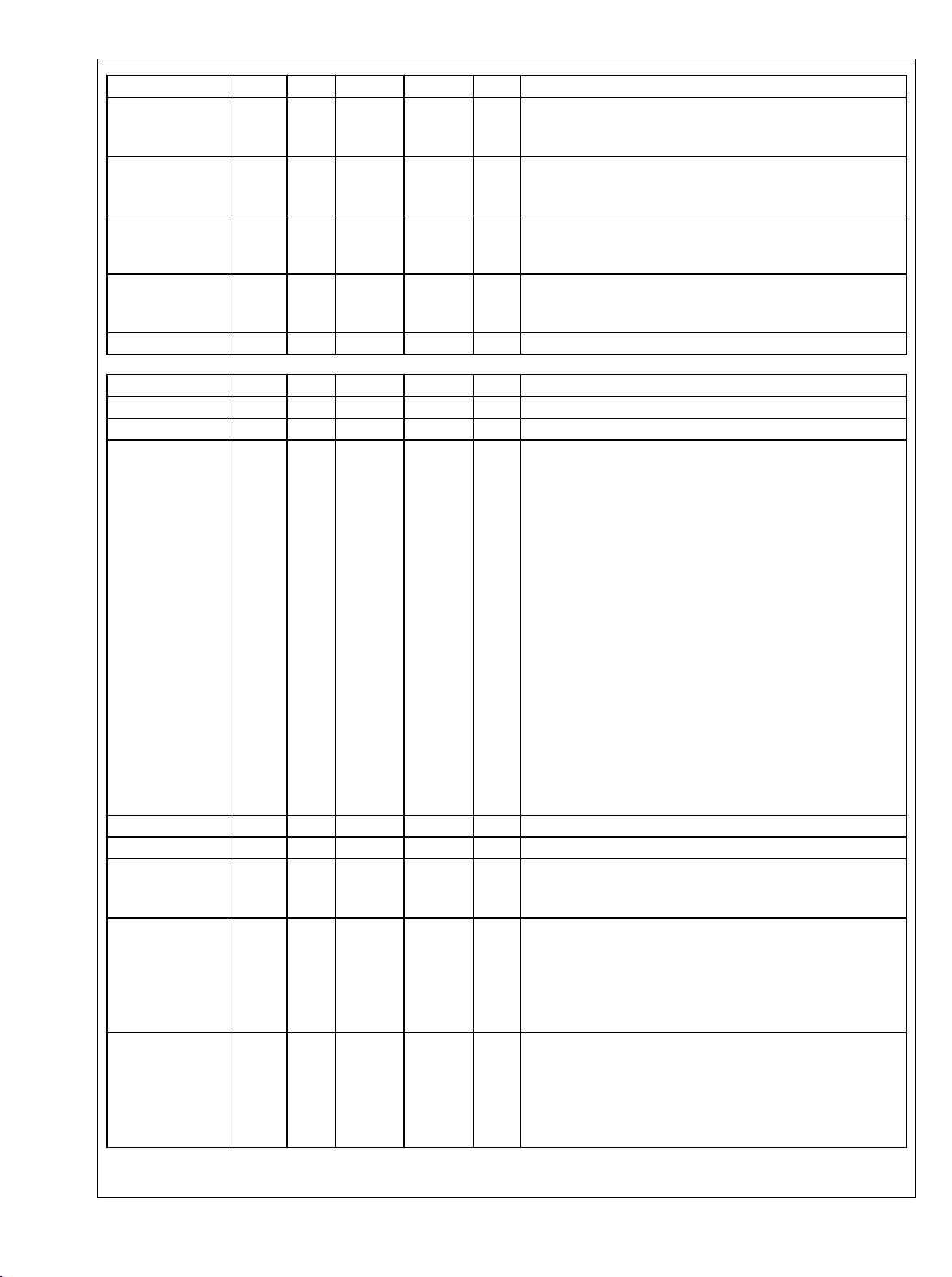
a
Register Name Width Type
Default
Addr Bit Description
AGC fixed gain for channel B. Format is an 8-bit, unsigned
AGC_IC_B 1B R/W 0 24 7:0
LM97593
magnitude number. The channel B DVGA gain will be set to the
inverted three MSBs.
AGC integrator readback value for channel A. Format is an 8-
AGC_RB_A 1B R 0 25 7:0
bit, unsigned magnitude number. The user can read the
magnitude MSBs of the channel A integrator from this register.
AGC integrator readback value for channel B. Format is an 8-
AGC_RB_B 1B R 0 26 7:0
bit, unsigned magnitude number. The user can read the
magnitude MSBs of the channel B integrator from this register.
Test input source. Instead of processing values from the
7:0
A|BIN pins, the value from this location is used instead. Format
5:0
is 14-bit 2s complement number spread across 2 registers.
TEST_REG 14b R/W 0
27(LSBs)
28(MSBs)
Reserved 1B - - 29 7:0 For future use.
a
Register Name Width Type
Default
Addr Bit Description
Reserved 1B - - 30 7:0 For future use
DEBUG_EN 1b R/W 0 31 0 0=Normal. 1=Enables access to the internal probe points.
Selects internal node tap for debug.
0 selects F1 output for BI, 20 bits
1 selects F1 output for BQ, 20 bits
2 selects F1 output for AQ, 20 bits
3 selects F1 output for AI, 20 bits
4 selects F1 input for BI, 20 bits
5 selects F1 input for BQ, 20 bits
6 selects F1 input for AI, 20 bits
7 selects F1 input for AQ, 20 bits
DEBUG_TAP 5b R/W 0 31 5:1
8 selects NCO A, cosine output. 17 bits, 3 LSBs are 0.
9 selects NCO A, sine output, 17 bits, 3 LSBs are 0.
10 selects NCO B, cosine output, 17 bits, 3 LSBs are 0.
11 selects NCO B, sine output, 17 bits, 3 LSBs are 0.
12 selects NCO AI, rounded output, 15 bits, 5 LSBs are 0.
13 selects NCO AQ, rounded output, 15 bits, 5 LSBs are 0.
14 selects NCO BI, rounded output, 15 bits, 5 LSBs are 0.
15 selects NCO BQ, rounded output, 15 bits, 5 LSBs are 0.
16 selects AGC CIC filter output. 9 MSBs from ch A, next 9 bits
from ch B, 2 LSBs are 0.
17-31 Reserved.
DITH_A 1b R/W 1 31 6 0=Disable NCO dither source for channel A. 1=Enable.
DITH_B 1b R/W 1 31 7 0=Disable NCO dither source for channel B. 1=Enable.
RAM space that defines key AGC loop parameters. Format is
AGC_TABLE 32B R/W 0 128-159 7:0
32 separate 8-bit, 2’s complement numbers. This is common to
both channels.
Coefficients for F1. Format is 11 separate 16-bit, 2’s
complement numbers, each one spread across 2 registers. The
F1_COEFF 22B R/W 0 160-181 7:0
LSBs are in the lower registers. For example, coefficient h0[7:0]
is in address 160, h0[15:8] is in address 161, h1[7:0] is in
address 162, h1[15:8] is in address 163. PAGE_SEL_F1=1
maps these addresses to coefficient memory B.
Coefficients for F2. Format is 32 separate 16-bit, 2’s
complement numbers, each one spread across 2 registers. The
F2_COEFF 64B R/W 0 182-245 7:0
LSBs are in the lower registers. For example, coefficient h0[7:0]
is in address 182, h0[15:8] is in address 183, h1[7:0] is in
address 184, h1[15:8] is in address 185. PAGE_SEL_F2=1
maps these addresses to coefficient memory B.
www.national.com 38
Page 39

a
Register Name Width Type
COEF_SEL_F1A 1b R/W 0 246 0
COEF_SEL_F1B 1b R/W 0 246 1
Default
Addr Bit Description
Channel A F1 coefficient select register. 0=memory A,
1=memory B.
Channel B F1 coefficient select register. 0=memory A,
1=memory B.
PAGE_SEL_F1 1b R/W 0 246 2 F1 coefficient page select register. 0=memory A, 1=memory B.
COEF_SEL_F2A 1b R/W 0 247 0
COEF_SEL_F2B 1b R/W 0 247 1
Channel A F2 coefficient select register. 0=memory A,
1=memory B.
Channel B F2 coefficient select register. 0=memory A,
1=memory B.
PAGE_SEL_F2 1b R/W 0 247 2 F2 coefficient page select register. 0=memory A, 1=memory B.
0=SFS asserted at the start of each output word when
SFS_MODE 1b R/W 0 248 0
PACKED=1 or each I/Q pair when PACKED=0, 1=SFS asserted
at the start of each output sample period.
a
Register Name Width Type
Default
Addr Bit Description
SDC_EN 1b R/W 0 248 1 0=normal serial mode, 1=serial daisy-chain master mode.
Enable reduced bandwidth AGC power detector. 0=2nd-order
AGC_COMB_ORD 2b R/W 0 249 1:0
decimate-by-eight CIC, 1=1-tap comb added to CIC, 2=4-tap
comb added to CIC.
Number of CK period delays needed to align the DVGA gain
EXT_DELAY 5b R/W 0 249 6:2
step with the digital gain compensation step. Set this register to
7 if ASTROBE and BSTROBE are not used. Otherwise set to 8.
LM97593
a. These are the default values set by a master reset (MR). Sync in (SI) will not affect any of these values.
9.2 Condensed LM97593 Address Map
Register
Name
Addr
Addr
Hex
Bit7 Bit6 Bit5 Bit4 Bit3 Bit2 Bit1 Bit0
DEC 0 0x00 Dec7 Dec6 Dec5 Dec4 Dec3 Dec2 Dec1 Dec0
DEC_BY_4 1 0x01 DecBy4 Dec10 Dec9 Dec8
SCALE 2 0x02 Sc5 Sc4 Sc3 Sc2 Sc1 Sc0
GAIN_A 3 0x03 GA2 GA1 GA0
GAIN_B 4 0x04 GB2 GB1 GB0
RATE 5 0x05 Rate7 Rate6 Rate5 Rate4 Rate3 Rate2 Rate1 Rate0
SERIAL_CTRL 6 0x06 FMT1 FMT0 Packed MuxMode RDY_POL SFS_POL SCK_POL SOUT_EN
FREQ_A 7 0x07 FA7 FA6 FA5 FA4 FA3 FA2 FA1 FA0
8 0x08 FA15 FA14 FA13 FA12 FA11 FA10 FA9 FA8
9 0x09 FA23 FA22 FA21 FA20 FA19 FA18 FA17 FA16
10 0x0A FA31 FA30 FA29 FA28 FA27 FA26 FA25 FA24
PHASE_A 11 0x0B PA7 PA6 PA5 PA4 PA3 PA2 PA1 PA0
12 0x0C PA15 PA14 PA13 PA12 PA11 PA10 PA9 PA8
FREQ_B 13 0x0D FB7 FB6 FB5 FB4 FB3 FB2 FB1 FB0
14 0x0E FB15 FB14 FB13 FB12 FB11 FB10 FB9 FB8
15 0x0F FB23 FB22 FB21 FB20 FB19 FB18 FB17 FB16
16 0x10 FB31 FB30 FB29 FB28 FB27 FB26 FB25 FB24
PHASE_B 17 0x11 PB7 PB6 PB5 PB4 PB3 PB2 PB1 PB0
18 0x12 PB15 PB14 PB13 PB12 PB11 PB10 PB9 PB8
Source 19 0x13 BS1 BS0 AS1 AS0
AGC_CTRL 20 0x14 AgcLG1 AgcLG0 AgcHldlC Reserved Reserved Explnh
AGC_COUNT 21 0x15 Reserved Reserved Reserved Reserved Reserved Reserved Reserved Reserved
22 0x16 Reserved Reserved Reserved Reserved Reserved Reserved Reserved Reserved
39 www.national.com
Page 40
Register
Name
AGC_IC_A 23 0x17 AgclcA7 AgclcA6 AgclcA5 AgclcA4 AgclcA3 AgclcA2 AgclcA1 AgclcA0
LM97593
AGC_IC_B 24 0x18 AgclcB7 AgclcB6 AgclcB5 AgclcB4 AgclcB3 AgclcB2 AgclcB1 AgclcB0
AGC_RB_A 25 0x19 AgcRbA7 AgcRbA6 AgcRbA5 AgcRbA4 AgcRbA3 AgcRbA2 AgcRbA1 AgcRbA0
AGC_RB_B 26 0x1A AGCRbB7 AGCRbB6 AGCRbB5 AGCRbB4 AGCRbB3 AGCRbB2 AGCRbB1 AGCRbB0
TEST_REG 27 0x1B Test7 Test6 Test5 Test4 Test3 Test2 Test1 Test0
28 0x1C Test13 Test12 Test11 Test10 Test9 Test8
DEBUG 31 0x1F DITH_B DITH_A TapSel4 TapSel3 TapSel2 TapSel1 TapSel0 DebugEnable
AGC_TABLE 128 0x80 The AGC Table loads from the low address to the high address in this order:
159 0x9F
Addr
Addr
Hex
Bit7 Bit6 Bit5 Bit4 Bit3 Bit2 Bit1 Bit0
"1st location, 2nd location..."
Register Name Addr
F1_COEFF 160 0xA0 The FIR Coefficients load from the low address to the high address in this order:
181 0xB5
F2COEFF 182 0xB6
245 0xF5
F1_CTRL 246 0xF6 PgSelF1 CfSelF1B CfSelF1A
F2_CTRL 247 0xF7 PgSelF2 CfSelF2B CfSelF2A
SERIAL_CTRL2 248 0xF8 SdcEn SfsMode
AGC_CTRL2 249 0xF9 ExtDelay4 ExtDelay3 ExtDelay2 ExtDelay1 ExtDelay0 CombOrd1 CombOrd0
Addr
Hex
Bit7 Bit6 Bit5 Bit4 Bit3 Bit2 Bit1 Bit0
"1st location low byte, 1st location high byte, 2nd location...""
The Page Select bits determine which set of coefficient memory is written.
www.national.com 40
Page 41

LM97593
AGC Theory of Operation
A block diagram of the AGC is shown in Figure 40. The DVGA
interface comprises four pins for each of the channels. The
first three pins of this interface are a 3-bit binary word that
controls the DVGA gain in 6dB steps (AGAIN). The final pin
is ASTROBE
the DVGA’s register. A key feature of the ASTROBE, illustrated Figure 41, is that it toggles only if the data on AGAIN
has changed from the previous cycle. Not shown is that AS-
TROBE and BSTROBE are independent. For example, ASTROBE only toggles when AGAIN has changed.
BSTROBE will not toggle because AGAIN has changed. This
is done to minimize unnecessary digital noise on the sensitive
analog path through the DVGA. ASTROBE and BSTROBE
are asserted during MR and SI to properly initialize the DVGAs.
The absolute value circuit and the 2-stage, decimate-by-8
CIC filter comprise the power detection part of the AGC. The
power detector bandwidth is set by the CIC filter to FCK/8. The
absolute value circuit doubles the effective input frequency.
This has the effect of reducing the power detector bandwidth
from FCK/8 to FCK/16.
For a full-scale sinusoidal input, the absolute value circuit
output is a dc value of 511*(2/π). Because the absolute value
which allows the AGAIN bits to be latched into
circuit also generates undesired even harmonic terms, the
CIC filter (response shown in Figure 39) is required to remove
these harmonics. The first response null occurs at
30008736
FIGURE 39. Power detector filter response, 52 MHz
30008737
FIGURE 40. LM97593 AGC circuit, Channel A
30008738
FIGURE 41. Timing diagram for AGC/DVGA interface, Channel A. Refer to Figure 7 for detailed timing information.
41 www.national.com
Page 42

FCK/8, where FCK is the clock frequency, and the response
magnitude is at least 25dB below the dc value from FCK/10 to
9FCK/10. Because the 2nd harmonic from the absolute value
LM97593
circuit is about 10dB below the dc this means that the ripple
in the detected level is about 0.7dB or less for input frequencies between FCK/20 to 19FCK/20. Setting the
AGC_COMB_ORD register to either 1 or 2 will narrow the
power detector’s bandwidth as shown in Figure 39.
The “FIXED TO FLOAT CONVERTER” takes the fixed point
9-bit output from the CIC filter and converts it to a “floating
point” number. This conversion is done so that the 32 values
in the RAM can be uniformly assigned (dB scale) to detected
power levels (54 dB range). This provides a resolution of
1.7dB between detected power levels. The truth table for this
converter is given in Table 4. The upper three bits of the output represent the exponent (e) and the lower 2 are the mantissa (m). The exponent is determined by the position of the
leading ‘1’ out of the CIC filter. An output of ‘001XX’ corresponds to a leading ‘1’ in bit 2 (LSB is bit 0). The exponent
increases by one each time the leading ‘1’ advances in bit
position. The mantissa bits are the two bits that follow the
leading ‘1’. If we define E as the decimal value of the exponent
bits and M as the decimal value of the mantissa bits, the output of the CIC filter, POUT, corresponding to a given “FIXED
TO FLOAT CONVERTER” output is:
The max() and min() operators account for row 1 of Table 4
which is a special case because M=P
ciates each address of the RAM with a CIC filter output.
. Equation 5 asso-
OUT
TABLE 4. Fixed to Float Converter Truth Table
INPUT OUTPUT (eeemm)
0-3 000XX
4-7 001XX
8-15 010XX
16-31 011XX
32-63 100XX
64-127 101XX
128-255 110XX
256-511 111XX
As shown in Figure 40, the 32X8 RAM look-up table implements the functions of log converter, reference subtraction,
error amplifier, and deadband. The user must build each of
these functions by constructing a set of 8-bit, 2’s complement
numbers to be loaded into the RAM. Each of these functions
and how to construct them are discussed in the following
paragraphs.
A log conversion is done in order to keep the loop gain independent of operating point. To see why this is beneficial, the
control gain of the DVGA computed without log conversion is:
(Eq. 9)
(Eq. 10)
that the DVGA gain control polarity is positive as is the case
for the CLC5526. The gain around the entire loop must be
negative. Observe in Equation 6 that the control gain is dependent on operating point G. If we instead compute the
control gain with log conversion then:
(Eq. 11)
which is no longer operating-point dependent. The log function is constructed by computing the CIC filter output associated with each address (Equation 5) and converting these to
dB. Full scale (dc signal) is 20log(511)=54dB.
The reference subtraction is constructed by subtracting the
desired loop servo point (in dB) from the table values computed in the previous paragraph. For example, if it is desired
that the DVGA servo the ADC input level (sinusoidal signal)
to -6dBFS, the number to subtract from the data is:
(Eq. 12)
The table data will then cross through zero at the address
corresponding to this reference level. A deadband wider than
6dB should then be constructed symmetrically about this
point. This prevents the loop from hunting due to the 6dB gain
steps of the DVGA. Any deadband in excess of 6dB appears
as hysteresis in the servo point of the loop as illustrated in
Figure 37. The deadband is constructed by loading zeros into
those addresses on either side of the one which corresponds
to the reference level.
The last function of the RAM table is that of error amplification.
All the operations preceding this one gave a table slope
S
= 1. This must now be adjusted in order to control the
RAM
time constant of the loop given by:
(Eq. 13)
The term GL in this equation is the loop gain:
(Eq. 14)
The design equations are obtained by solving Equation 13 for
GL and Equation 14 for S
register value that determines the number of bits to shift the
. AGC_LOOP_GAIN is a control
RAM
output of the RAM down by. This allows some of the loop gain
to be moved out of the RAM so that the full output range of
the table is utilized but not exceeded. The valid range for
AGC_LOOP_GAIN is from 0 to 3 which corresponds to a 0 to
3 bit shift to the left.
An example set of numbers to implement a loop having a reference of 6dB below full scale, a deadband of 8dB, and a loop
gain of 0.108 is:
-102 -102 -88 -80 -75 -70 -66
-63 -61 -56 -53 -50
-47 -42 -39 -36 -33 -29 -25
-22 -19 -15 -11 -0
0 0 0 0 0 13 17 20
where G is the decimal equivalent of GAIN and Go accounts
for the DVGA gain in excess of unity. This equation assumes
www.national.com 42
Page 43

LM97593
30008740
30008739
FIGURE 43. Example of programmed RAM contents
FIGURE 42. Example of programmed RAM contents
TABLE 5. 15-bit Mixer Output Alignment into the 22-bit SHIFT-UP Based On EXP
AGAIN
a
EXP
b
Input
c
d
21
20 19 18 17 16 15 14 ... 8 7 6 5 4 3 2 1 0
000 = -12dB 111 = +0dB -12dB 14 13 12 11 10 9 8 7 ... 1 0 L L L L L L L
001 = -6dB 110 = -6dB -12dB 14 14 13 12 11 10 9 8 ... 2 1 0 L L L L L L
010 = 0dB 101 = -12dB -12dB 14 14 14 13 12 11 10 9 ... 3 2 1 0 L L L L L
011 = +6dB 100 = -18dB -12dB 14 14 14 14 13 12 11 10 ... 4 3 2 1 0 L L L L
100 = +12dB 011 = -24dB -12dB 14 14 14 14 14 13 12 11 ... 5 4 3 2 1 0 L L L
101 = +18dB 010 = -30dB -12dB 14 14 14 14 14 14 13 12 ... 6 5 4 3 2 1 0 L L
110 = +24dB 001 = -36dB -12dB 14 14 14 14 14 14 14 13 ... 7 6 5 4 3 2 1 0 L
111 = +30dB 000 = -42dB -12dB 14 14 14 14 14 14 14 14 ... 8 7 6 5 4 3 2 1 0
a. AGAIN sets the DVGA or analog gain value.
b. EXP sets the "FIXED TO FLOAT CONVERTER" or digital gain value.
c. 22-bit input to SHIFT-UP block in Figure 19 horizontally, linearized SHIFT-UP value vertically.
d. The numbers in the center of the table represent the mixer output bits. 'L' represents a logic low.
These values are shown with respect to the table addresses
in Figure 42, and the CIC filter output P
a 52MHz clock rate and AGC_LOOP_GAIN=2, these values
in Figure 43. For
OUT
result in a loop time constant of 1.5µs.
The error signal from the loop gain “SHIFT DOWN” circuit is
gated into the loop integrator. A MUX within the integrator
feedback allows the integrator to be initialized to the value
loaded into AGC_IC_A (channel B can be set independently).
The top eight bits of the integrator output can also be read
back over the microprocessor interface from the AGC_RB_A
(or AGC_RB_B) register. The top 3 bits become AGAIN and
are output along with the ASTROBE signal on the DVGA interface pins. The valid range of AGAIN is from 0 to 7 which
corresponds to a valid range of 0 to 211-1 for the 11-bit, 2’s
complement integrator output from which AGAIN is derived.
This is illustrated in Figure 44. The integrator saturates at
these limits to prevent overshoots as the integrator attempts
to enter the valid range. The AGAIN value is inverted (EXP)
and used to adjust the gain of the incoming signal to provide
a linear output dynamic range. The relationship between the
DVGA analog gain (AGAIN) and the “FIXED TO FLOAT
CONVERTER” digital gain (EXP) is shown in Table 5. The
DVGA’s compression of the incoming signal in the analog
domain vs. the subsequent expansion in the digital domain is
shown in Figure 36.
The AGC may be forced to free run by setting AGC_HOLD_IC
low. Writing an initial condition to AGC_IC_A|B and then setting AGC_HOLD_IC high will force the AGC to a fixed gain.
The three MSBs of the value written to AGC_IC_A|B are inverted and output to drive the DVGA.
Allowing the AGC to free run should be appropriate for most
applications. If the INH_EXP bit is not set, the DVGA gain
word (EXP) is routed to the “FLOAT TO FIXED CONVERTER” in the DDCs prior to the programmable decimation filter.
The EXP signals are delayed to account for the propagation
delay of the DVGA interface and the ADC12DL080 ADC.
43 www.national.com
Page 44

General Applications Information
LM97593
10.0 OUTPUTS
Be very careful when driving a high capacitance bus. The
more capacitance the output drivers must charge for each
conversion, the more instantaneous digital current flows
through VDR and DRGND. These large charging current
spikes can cause on-chip ground noise and couple into the
analog circuitry, degrading dynamic performance. Adequate
bypassing, limiting output capacitance and careful attention
to the ground plane will reduce this problem.
To minimize noise due to output switching, minimize the load
currents at the digital outputs. Only one driven input should
be connected to each output pin. Additionally, inserting series
resistors of about 100Ω at the digital outputs, close to the ADC
pins, will isolate the outputs from trace and other circuit capacitances and limit the output currents, which could otherwise result in performance degradation. See Figure 45.
30008741
FIGURE 44. AGC integrator output limits
www.national.com 44
Page 45

LM97593
FIGURE 45. Application Circuit
45 www.national.com
30008757
Page 46

11.0 POWER SUPPLY CONSIDERATIONS
The power supply pins should be bypassed with a 10 µF capacitor and with a 0.1 µF ceramic chip capacitor near each
LM97593
power pin. Leadless chip capacitors are preferred because
they have low series inductance.
The LM97593 is sensitive to power supply noise. Accordingly,
the noise on the analog supply pins should be kept below 100
mV
.
P-P
No pin should ever have a voltage on it that is in excess of the
supply voltages, not even on a transient basis. Be especially
careful of this during power turn on and turn off.
The VDR pin provides power for the output drivers and should
be operated from a supply equivalent to VD.
12.0 LAYOUT AND GROUNDING
A proper grounding and proper routing of all signals are essential to ensure accurate conversion. Maintaining separate
analog and digital areas of the board, with the LM97593 between these areas, is required to achieve specified performance.
The ground return for the data outputs (DRGND) carries the
ground current for the output drivers. The output current can
exhibit high transients that could add noise to the conversion
process. To prevent this from happening, the DRGND pins
should NOT be connected to system ground in close proximity
to any of the LM97593's other ground pins.
Capacitive coupling between the typically noisy digital circuitry and the sensitive analog circuitry can lead to poor performance. The solution is to keep the analog circuitry separated
from the digital circuitry, and to keep the clock line as short as
possible.
Digital circuits create substantial supply and ground current
transients. The logic noise thus generated could have significant impact upon system noise performance. The best logic
family to use in systems with A/D converters is one which
employs non-saturating transistor designs, or has low noise
characteristics, such as the 74LS, 74HC(T) and 74AC(T)Q
families. The worst noise generators are logic families that
create the largest supply current transients during clock or
signal edges, like the 74F and the 74AC(T) families.
The effects of the noise generated from the LM97593 output
switching can be minimized through the use of 100Ω resistors
in series with each data output line. Locate these resistors as
close to the LM97593 output pins as possible.
Since digital switching transients are composed largely of
high frequency components, total ground plane copper
weight will have little effect upon the logic-generated noise.
This is because of the skin effect. Total surface area is more
important than is total ground plane volume.
Generally, analog and digital lines should cross each other at
90° to avoid crosstalk. To maximize accuracy in high speed,
high resolution systems, however, avoid crossing analog and
digital lines altogether. It is important to keep clock lines as
short as possible and isolated from ALL other lines, including
other digital lines. Even the generally accepted 90° crossing
should be avoided with the clock line as even a little coupling
can cause problems at high frequencies. This is because other lines can introduce jitter into the clock line, which can lead
to degradation of SNR. Also, the high speed clock can introduce noise into the analog chain.
Best performance at high frequencies and at high resolution
is obtained with a straight signal path. That is, the signal path
through all components should form a straight line wherever
possible.
Be especially careful with the layout of inductors. Mutual inductance can change the characteristics of the circuit in which
they are used. Inductors should not be placed side by side,
even with just a small part of their bodies beside each other.
The analog input should be isolated from noisy signal traces
to avoid coupling of spurious signals into the input. Any external component (e.g., a filter capacitor) connected between
the converter's input pins and ground or to the reference input
pin and ground should be connected to a very clean point in
the ground plane.
All analog circuitry (input amplifiers, filters, reference components, etc.) should be placed in the analog area of the board.
All digital circuitry and I/O lines should be placed in the digital
area of the board. The LM97593 should be between these
two areas. Furthermore, all components in the reference circuitry and the input signal chain that are connected to ground
should be connected together with short traces and enter the
ground plane at a single, quiet point. All ground connections
should have a low inductance path to ground.
13.0 DYNAMIC PERFORMANCE
To achieve the best dynamic performance, the clock source
driving the CLK input must be free of jitter. Isolate the ADC
clock from any digital circuitry with buffers, as with the clock
tree shown in Figure 46. The gates used in the clock tree must
be capable of operating at frequencies much higher than
those used if added jitter is to be prevented.
Best performance will be obtained with a differential input
drive, compared with a single-ended drive, as discussed in
Sections 1.3.1 and 1.3.2.
It is good practice to keep the clock line as short as possible
and to keep it well away from any other signals. Other signals
can introduce jitter into the clock signal, which can lead to
reduced SNR performance, and the clock can introduce noise
into other lines. Even lines with 90° crossings have capacitive
coupling, so try to avoid even these 90° crossings of the clock
line.
30008756
FIGURE 46. Isolating the ADC Clock from other Circuitry
with a Clock Tree
www.national.com 46
Page 47

LM97593
Common Application Pitfalls
15.1 Driving the inputs (analog or digital) beyond the
power supply rails. For proper operation, all inputs should
not go more than 100 mV beyond the supply rails (more than
100 mV below the ground pins or 100 mV above the supply
pins). Exceeding these limits on even a transient basis may
cause faulty or erratic operation. It is not uncommon for high
speed digital components (e.g., 74F and 74AC devices) to
exhibit overshoot or undershoot that goes above the power
supply or below ground. A resistor of about 47Ω to 100Ω in
series with any offending digital input, close to the signal
source, will eliminate the problem.
Do not allow input voltages to exceed the supply voltage, even
on a transient basis. Not even during power up or power
down.
Be careful not to overdrive the inputs of the LM97593 with a
device that is powered from supplies outside the range of the
LM97593 supply. Such practice may lead to conversion inaccuracies and even to device damage.
15.2 Attempting to drive a high capacitance digital data
bus. The more capacitance the output drivers must charge
for each conversion, the more instantaneous digital current
flows through VDR and DRGND. These large charging current
spikes can couple into the analog circuitry, degrading dynamic performance. Adequate bypassing and maintaining separate analog and digital areas on the pc board will reduce this
problem.
The digital data outputs should be buffered (with 74ACQ541,
for example) if they will drive a large capacitive load. Dynamic
performance can also be improved by adding series resistors
at each digital output, close to the LM97593, which reduces
the energy coupled back into the part's output pins by limiting
the output current. A reasonable value for these resistors is
100Ω.
15.3 Using an inadequate amplifier to drive the analog
input. As explained in Section 1.3, the capacitance seen at
the input alternates between 8 pF and 7 pF, depending upon
the phase of the clock. This dynamic load is more difficult to
drive than is a fixed capacitance. If the amplifier exhibits overshoot, ringing, or any evidence of instability, even at a very
low level, it will degrade performance. A small series resistor
at each amplifier output and a capacitor at the analog inputs
will improve performance.
Also, it is important that the signals at the two inputs have
exactly the same amplitude and be exactly 180º out of phase
with each other. Board layout, especially equality of the length
of the two traces to the input pins, will affect the effective
phase between these two signals. Remember that an operational amplifier operated in the non-inverting configuration will
exhibit more time delay than will the same device operating
in the inverting configuration.
15.4 Operating with the reference pins outside of the
specified range. As mentioned in Section 1.2, V
be in the range of
0.8V ≤ V
Operating outside of these limits could lead to performance
degradation.
15.5 Inadequate network on Reference Bypass pins
(VRPA, VRNA, V
tioned in Section 1.2, these pins should be bypassed with 0.1
µF capacitors to ground at VRMA and VRMB and with a 10 µF
between pins VRPA and VRNA and between VRPB and VRNB
for best performance.
15.6 Using a clock source with excessive jitter, using excessively long clock signal trace, or having other signals
coupled to the clock signal trace. This will cause the sam-
pling interval to vary, causing excessive output noise and a
reduction in SNR and SINAD performance.
A, VRPB, VRNB and V
COM
REF
≤ 1.2V
COM
should
REF
B). As men-
Evaluation Hardware
Evaluation boards are available to facilitate designs based on
the LM97593:
16.1 LM97593EB
The LM97593 evaluation board provides a complete narrowband receiver from IF to digital symbols.
16.2 SOFTWARE
Control panel software for the LM97593 supports complete
device configuration on both evaluation boards.
Integrated capture software manages the capture of data and
its storage in a file on a PC.
Matlab script files support data analysis: FFT, DNL, and INL
plotting.
This software and additional application information is available on the Basestation CDROM.
47 www.national.com
Page 48

Physical Dimensions inches (millimeters) unless otherwise noted
LM97593
LM97593VH PQFP Package Dimensions
www.national.com 48
Page 49

Notes
LM97593
49 www.national.com
Page 50

Notes
For more National Semiconductor product information and proven design tools, visit the following Web sites at:
Products Design Support
Amplifiers www.national.com/amplifiers WEBENCH www.national.com/webench
Audio www.national.com/audio Analog University www.national.com/AU
Clock Conditioners www.national.com/timing App Notes www.national.com/appnotes
Data Converters www.national.com/adc Distributors www.national.com/contacts
Displays www.national.com/displays Green Compliance www.national.com/quality/green
Ethernet www.national.com/ethernet Packaging www.national.com/packaging
Interface www.national.com/interface Quality and Reliability www.national.com/quality
LVDS www.national.com/lvds Reference Designs www.national.com/refdesigns
Power Management www.national.com/power Feedback www.national.com/feedback
Switching Regulators www.national.com/switchers
LDOs www.national.com/ldo
LED Lighting www.national.com/led
PowerWise www.national.com/powerwise
Serial Digital Interface (SDI) www.national.com/sdi
LM97593 Dual ADC / Digital Tuner / AGC
Temperature Sensors www.national.com/tempsensors
Wireless (PLL/VCO) www.national.com/wireless
THE CONTENTS OF THIS DOCUMENT ARE PROVIDED IN CONNECTION WITH NATIONAL SEMICONDUCTOR CORPORATION
(“NATIONAL”) PRODUCTS. NATIONAL MAKES NO REPRESENTATIONS OR WARRANTIES WITH RESPECT TO THE ACCURACY
OR COMPLETENESS OF THE CONTENTS OF THIS PUBLICATION AND RESERVES THE RIGHT TO MAKE CHANGES TO
SPECIFICATIONS AND PRODUCT DESCRIPTIONS AT ANY TIME WITHOUT NOTICE. NO LICENSE, WHETHER EXPRESS,
IMPLIED, ARISING BY ESTOPPEL OR OTHERWISE, TO ANY INTELLECTUAL PROPERTY RIGHTS IS GRANTED BY THIS
DOCUMENT.
TESTING AND OTHER QUALITY CONTROLS ARE USED TO THE EXTENT NATIONAL DEEMS NECESSARY TO SUPPORT
NATIONAL’S PRODUCT WARRANTY. EXCEPT WHERE MANDATED BY GOVERNMENT REQUIREMENTS, TESTING OF ALL
PARAMETERS OF EACH PRODUCT IS NOT NECESSARILY PERFORMED. NATIONAL ASSUMES NO LIABILITY FOR
APPLICATIONS ASSISTANCE OR BUYER PRODUCT DESIGN. BUYERS ARE RESPONSIBLE FOR THEIR PRODUCTS AND
APPLICATIONS USING NATIONAL COMPONENTS. PRIOR TO USING OR DISTRIBUTING ANY PRODUCTS THAT INCLUDE
NATIONAL COMPONENTS, BUYERS SHOULD PROVIDE ADEQUATE DESIGN, TESTING AND OPERATING SAFEGUARDS.
EXCEPT AS PROVIDED IN NATIONAL’S TERMS AND CONDITIONS OF SALE FOR SUCH PRODUCTS, NATIONAL ASSUMES NO
LIABILITY WHATSOEVER, AND NATIONAL DISCLAIMS ANY EXPRESS OR IMPLIED WARRANTY RELATING TO THE SALE
AND/OR USE OF NATIONAL PRODUCTS INCLUDING LIABILITY OR WARRANTIES RELATING TO FITNESS FOR A PARTICULAR
PURPOSE, MERCHANTABILITY, OR INFRINGEMENT OF ANY PATENT, COPYRIGHT OR OTHER INTELLECTUAL PROPERTY
RIGHT.
LIFE SUPPORT POLICY
NATIONAL’S PRODUCTS ARE NOT AUTHORIZED FOR USE AS CRITICAL COMPONENTS IN LIFE SUPPORT DEVICES OR
SYSTEMS WITHOUT THE EXPRESS PRIOR WRITTEN APPROVAL OF THE CHIEF EXECUTIVE OFFICER AND GENERAL
COUNSEL OF NATIONAL SEMICONDUCTOR CORPORATION. As used herein:
Life support devices or systems are devices which (a) are intended for surgical implant into the body, or (b) support or sustain life and
whose failure to perform when properly used in accordance with instructions for use provided in the labeling can be reasonably expected
to result in a significant injury to the user. A critical component is any component in a life support device or system whose failure to perform
can be reasonably expected to cause the failure of the life support device or system or to affect its safety or effectiveness.
National Semiconductor and the National Semiconductor logo are registered trademarks of National Semiconductor Corporation. All other
brand or product names may be trademarks or registered trademarks of their respective holders.
Copyright© 2008 National Semiconductor Corporation
For the most current product information visit us at www.national.com
www.national.com
National Semiconductor
Americas Technical
Support Center
Email:
new.feedback@nsc.com
Tel: 1-800-272-9959
National Semiconductor Europe
Technical Support Center
Email: europe.support@nsc.com
German Tel: +49 (0) 180 5010 771
English Tel: +44 (0) 870 850 4288
National Semiconductor Asia
Pacific Technical Support Center
Email: ap.support@nsc.com
National Semiconductor Japan
Technical Support Center
Email: jpn.feedback@nsc.com
 Loading...