

查询LM95221供应商
LM95221
Dual Remote Diode Digital Temperature Sensor with
SMBus Interface
General Description
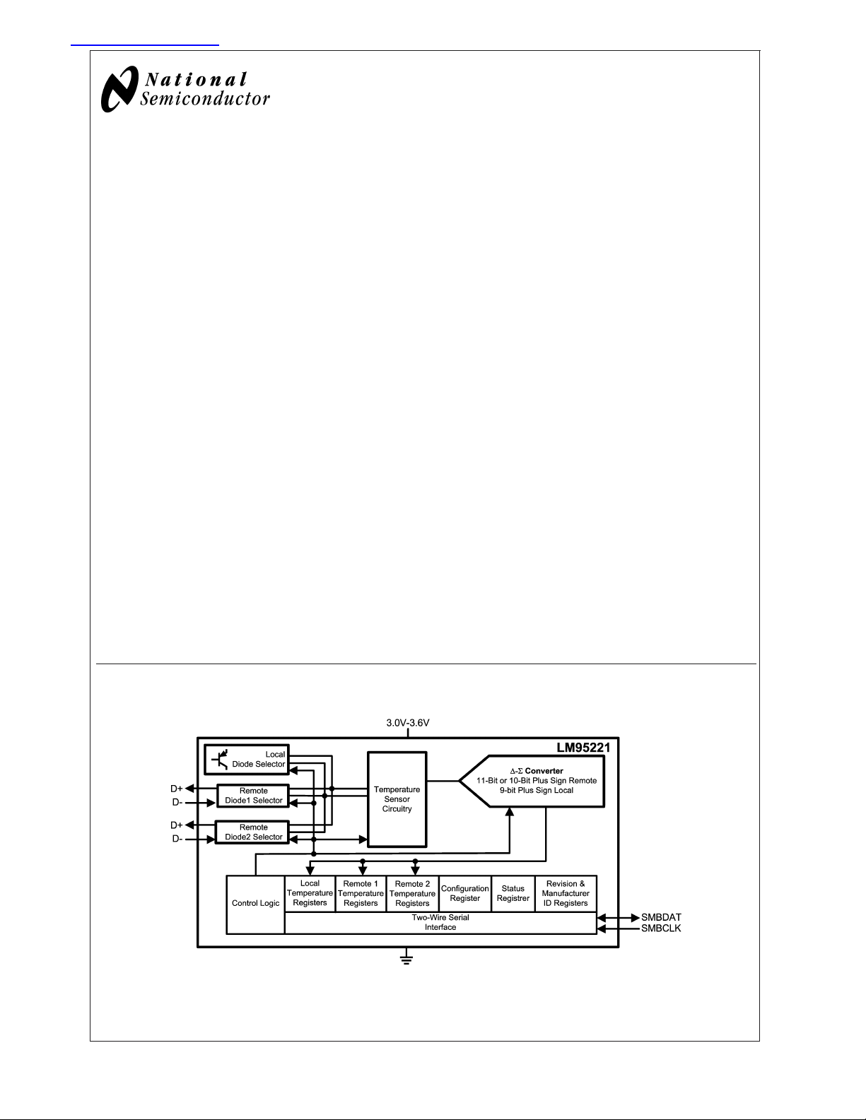
The LM95221 is a dual remote diode temperature sensor in
an 8-lead MSOP package. The 2-wire serial interface of the
LM95221 is compatible with SMBus 2.0. The LM95221 can
sense three temperature zones, it can measure the temperature of its own die as well as two diode connected transistors. The diode connected transistors can be a thermal diode
as found in Pentium and AMD processors or can simply be a
diode connected MMBT3904 transistor. The LM95221 resolution format for remote temperature readings can be programmed to be 10-bits plus sign or 11-bits unsigned. In the
unsigned mode the LM95221 remote diode readings can
resolve temperatures above 127˚C. Local temperature readings have a resolution of 9-bits plus sign.
The temperature of any ASIC can be accurately determined
using the LM95221 as long as a dedicated diode (semiconductor junction) is available on the target die. The LM95221
remote sensor accuracy of
series resistance of 2.7 ohms and 1.008 non-ideality factor.
±
1˚C is factory trimmed for a
Features
n Accurately senses die temperature of remote ICs or
diode junctions
n Remote diode fault detection
n On-board local temperature sensing
n Remote temperature readings:
— 0.125 ˚C LSb
— 10-bits plus sign or 11-bits programmable resolution
— 11-bits resolves temperatures above 127 ˚C
n Local temperature readings:
— 0.25 ˚C
— 9-bits plus sign
n Status register support
n Programmable conversion rate allows user optimization
of power consumption
n Shutdown mode one-shot conversion control
n SMBus 2.0 compatible interface, supports TIMEOUT
n 8-pin MSOP package
Key Specifications
j
Local Temperature Accuracy
T
=0˚C to 85˚C±3.0 ˚C (max)
A
j
Remote Diode Temperature Accuracy
T
=30˚C to 50˚C, TD=45˚C to 85˚C±1.0 ˚C (max)
A
T
=0˚C to 85˚C, TD=25˚C to 140˚C±3.0 ˚C (max)
A
j
Supply Voltage 3.0 V to 3.6 V
j
Supply Current 2 mA (typ)
Applications
n Processor/Computer System Thermal Management
(e.g. Laptop, Desktop, Workstations, Server)
n Electronic Test Equipment
n Office Electronics
LM95221 Dual Remote Diode Digital Temperature Sensor with SMBus Interface
May 2004
Simplified Block Diagram
20094301
Pentium™is a trademark of Intel Corporation.
© 2004 National Semiconductor Corporation DS200943 www.national.com
Connection Diagram
LM95221
MSOP-8
20094302
TOP VIEW
Ordering Information
Part Number
LM95221CIMM LM95221CIMM MUA08A (MSOP-8) 1000 Units on Tape
LM95221CIMMX LM95221CIMM MUA08A (MSOP-8) 3500 Units on Tape
Package
Marking
NS Package
Number
Pin Descriptions
Label Pin # Function Typical Connection
D1+ 1 Diode Current Source To Diode Anode. Connected to remote discrete
diode-connected transistor junction or to the
diode-connected transistor junction on a remote IC
whose die temperature is being sensed. A 2.2 nF
diode bypass capacitor is recommended to filter high
frequency noise. Place the 2.2 nF capacitor between
and as close as possible to the LM95221’s D+ and
D− pins. Make sure the traces to the 2.2 nF
capacitor are matched. Ground this pin if this
thermal diode is not used.
D1− 2 Diode Return Current Sink To Diode Cathode. A 2.2 nF capacitor is
recommended between D1+ and D1-. Ground this
pin if this thermal diode is not used.
D2+ 3 Diode Current Source To Diode Anode. Connected to remote discrete
diode-connected transistor junction or to the
diode-connected transistor junction on a remote IC
whose die temperature is being sensed. A 2.2 nF
diode bypass capacitor is recommended to filter high
frequency noise. Place the 2.2 nF capacitor between
and as close as possible to the LM95221’s D+ and
D− pins. Make sure the traces to the 2.2 nF
capacitor are matched. Ground this pin if this
thermal diode is not used.
D2− 4 Diode Return Current Sink To Diode Cathode. A 2.2 nF capacitor is
recommended between D2+ and D2-. Ground this
pin if this thermal diode is not used.
GND 5 Power Supply Ground Ground
V
DD
6 Positive Supply Voltage
Input
DC Voltage from 3.0 V to 3.6 V. VDDshould be
bypassed with a 0.1 µF capacitor in parallel with 100
pF. The 100 pF capacitor should be placed as close
as possible to the power supply pin. Noise should
be kept below 200 mVp-p, a 10 µF capacitor may be
required to achieve this.
Transport
Media
and Reel
and Reel
SMBus Device
Address
010 1011
010 1011
www.national.com 2
Pin Descriptions (Continued)
Label Pin # Function Typical Connection
SMBDAT 7 SMBus Bi-Directional Data
Line, Open-Drain Output
SMBCLK 8 SMBus Clock Input From Controller; may require an external pull-up
From and to Controller; may require an external
pull-up resistor
resistor
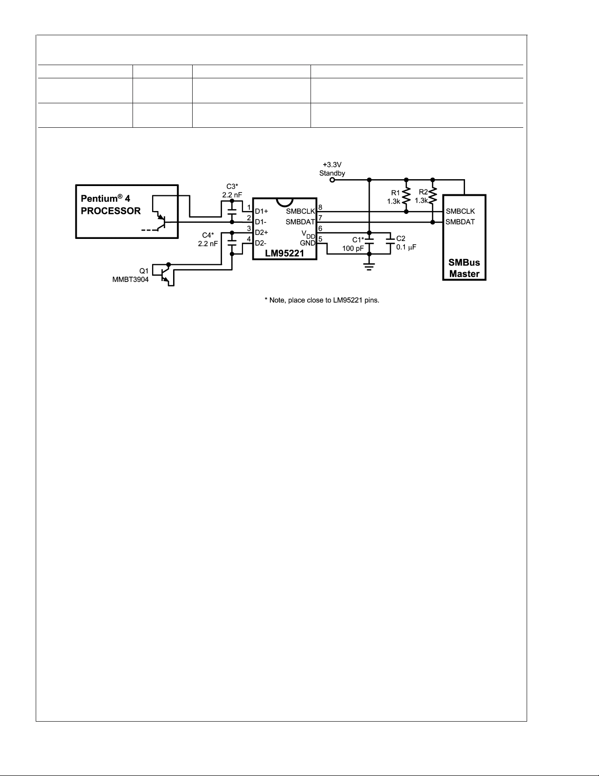
Typical Application
LM95221
20094303
www.national.com3
Absolute Maximum Ratings (Note 1)
Supply Voltage −0.3 V to 6.0 V
LM95221
Voltage at SMBDAT, SMBCLK −0.5V to 6.0V
Voltage at Other Pins −0.3 V to (V
D− Input Current
Input Current at All Other Pins (Note 2)
Package Input Current (Note 2) 30 mA
SMBDAT Output Sink Current 10 mA
Storage Temperature −65˚C to +150˚C
Soldering Information, Lead Temperature
MSOP-8 Package (Note 3)
Vapor Phase (60 seconds) 215˚C
DD
+ 0.3 V)
±
1mA
±
5mA
Infrared (15 seconds) 220˚C
ESD Susceptibility (Note 4)
Human Body Model 2000 V
Machine Model 200 V
Operating Ratings
(Notes 1, 5)
Operating Temperature Range 0˚C to +115˚C
Electrical Characteristics
Temperature Range T
LM95221CIMM 0˚C≤TA≤+85˚C
Supply Voltage Range (V
) +3.0V to +3.6V
DD
MIN≤TA≤TMAX
Temperature-to-Digital Converter Characteristics
Unless otherwise noted, these specifications apply for VDD=+3.0Vdc to 3.6Vdc. Boldface limits apply for TA=TJ=
T
MIN≤TA≤TMAX
junction temperature of the remote thermal diode.
Accuracy Using Local Diode T
Accuracy Using Remote Diode, see (Note 9) for
Thermal Diode Processor Type.
Remote Diode Measurement Resolution 11 Bits
Local Diode Measurement Resolution 10 Bits
Conversion Time of All Temperatures at the
Fastest Setting
Quiescent Current (Note 10) SMBus Inactive, 15Hz conversion
D− Source Voltage 0.7 V
Diode Source Current (D+ − D−)=+ 0.65V; high-level 188 315 µA (max)
Low-Level Diode Source Current Variation over
Temperature
Power-On Reset Threshold Measure on V
; all other limits TA=TJ=+25˚C, unless otherwise noted. TJis the junction temperature of the LM95221. TDis the
Parameter Conditions Typical Limits Units
(Note 6) (Note 7) (Limit)
= 0˚C to +85˚C, (Note 8)
A
T
= +30˚C to
A
+50˚C
= +0˚C to
T
A
+85˚C
TD= +45˚C
to +85˚C
TD= +25˚C
to +140˚C
±
1
±
3 ˚C (max)
±
1 ˚C (max)
±
3 ˚C (max)
0.125 ˚C
0.25 ˚C
(Note 11) 66 73 ms (max)
2.0 2.6 mA (max)
rate
Shutdown 335 µA
110 µA (min)
Low-level 11.75 20 µA (max)
7 µA (min)
T
= +30˚C to +50˚C +0.5 µA
A
T
= +30˚C to +85˚C +1.5 µA
A
edge
input, falling
DD
2.4
1.8
V (max)
V (min)
www.national.com 4

Logic Electrical Characteristics
DIGITAL DC CHARACTERISTICS Unless otherwise noted, these specifications apply for VDD=+3.0 to 3.6 Vdc. Boldface limits apply for T
A=TJ=TMIN
to T
Symbol Parameter Conditions Typical Limits Units
SMBDAT, SMBCLK INPUTS
V
IN(1)
V
IN(0)
V
IN(HYST)
Logical “1” Input Voltage 2.1 V (min)
Logical “0”Input Voltage 0.8 V (max)
SMBDAT and SMBCLK Digital Input
Hysteresis
I
I
C
IN(1)
IN(0)
IN
Logical “1” Input Current VIN=V
Logical “0” Input Current VIN= 0 V −0.005
Input Capacitance 5 pF
SMBDAT OUTPUT
I
OH
V
OL
High Level Output Current VOH=V
SMBus Low Level Output Voltage IOL= 4mA
SMBus DIGITAL SWITCHING CHARACTERISTICS Unless otherwise noted, these specifications apply for VDD=+3.0 Vdc to
+3.6 Vdc, C
(load capacitance) on output lines = 80 pF. Boldface limits apply for TA=TJ=T
L
=TJ= +25˚C, unless otherwise noted. The switching characteristics of the LM95221 fully meet or exceed the published specifications of the SMBus version 2.0. The following parameters are the timing relationships between SMBCLK and SMBDAT signals related to the LM95221. They adhere to but are not necessarily the SMBus bus specifications.
Symbol Parameter Conditions Typical Limits Units
f
t
t
HIGH
t
R,SMB
t
F,SMB
t
TIMEOUT
SMBus Clock Frequency 100
SMB
SMBus Clock Low Time from V
LOW
SMBus Clock High Time from V
SMBus Rise Time (Note 12) 1 µs (max)
SMBus Fall Time (Note 13) 0.3 µs (max)
t
Output Fall Time CL= 400pF,
OF
SMBDAT and SMBCLK Time Low for Reset of
Serial Interface (Note 14)
t
SU;DAT
t
HD;DAT
t
HD;STA
Data In Setup Time to SMBCLK High 250 ns (min)
Data Out Stable after SMBCLK Low 300
Start Condition SMBDAT Low to SMBCLK
Low (Start condition hold before the first clock
falling edge)
t
SU;STO
Stop Condition SMBCLK High to SMBDAT
Low (Stop Condition Setup)
t
SU;STA
SMBus Repeated Start-Condition Setup Time,
SMBCLK High to SMBDAT Low
t
SMBus Free Time Between Stop and Start
BUF
Conditions
; all other limits TA=TJ=+25˚C, unless otherwise noted.
MAX
(Note 6) (Note 7) (Limit)
400 mV
0.005
max 4.7
IN(0)
min 4.0 µs (min)
IN(1)
I
OL
DD
DD
= 6mA
IN(0)
IN(1)
= 3mA, (Note 13)
I
O
max to V
min to V
±
10 µA (max)
±
10 µA (max)
10 µA (max)
0.4
V (max)
0.6
MIN
to T
; all other limits T
MAX
(Note 6) (Note 7) (Limit)
kHz (max)
10
kHz (min)
µs (min)
25
ms (max)
250 ns (max)
25
35
ms (min)
ms (max)
ns (min)
900
ns (max)
100 ns (min)
100 ns (min)
0.6 µs (min)
1.3 µs (min)
LM95221
A
www.national.com5
SMBus Communication
LM95221
Note 1: Absolute Maximum Ratings indicate limits beyond which damage to the device may occur. DC and AC electrical specifications do not apply when operating
the device beyond its rated operating conditions.
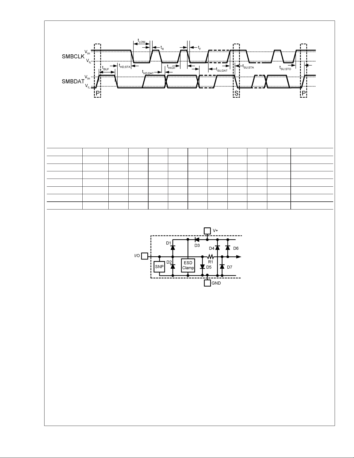
Note 2: When the input voltage (V
Parasitic components and or ESD protection circuitry are shown in the figure below for the LM95221’s pins. The nominal breakdown voltage of D4 is 6.5 V. Care
should be taken not to forward bias the parasitic diode, D1, present on pins: D1+, D2+, D1−, D2−. Doing so by more than 50 mV may corrupt the temperature
measurements.
) at any pin exceeds the power supplies (V
I
<
I
GND or V
Pin Name PIN # D1 D2 D3 D4 D5 D6 D7 R1 SNP ESD CLAMP
V
DD
1x x
D1+ 2 x x x x x x x
D1− 3 xx xxxxx x
D2+ 4 x x x x x x x
D2- 6 xx xxxxx x
SMBDAT 7 x x x x x
SMBCLK 8 x x x
>
VDD), the current at that pin should be limited to 5 mA.
I
20094309
Note: An “x” indicates that the component exists for the designated pin. SNP refers to a snap-back device.
20094313
FIGURE 1. ESD Protection Input Structure
Note 3: See the URL ”http://www.national.com/packaging/“ for other recommendations and methods of soldering surface mount devices.
Note 4: Human body model, 100pF discharged through a 1.5kΩ resistor. Machine model, 200pF discharged directly into each pin.
Note 5: Thermal resistance junction-to-ambient when attached to a printed circuit board with 2 oz. foil:
– MSOP-8 = 210˚C/W
Note 6: Typicals are at T
Note 7: Limits are guaranteed to National’s AOQL (Average Outgoing Quality Level).
Note 8: Local temperature accuracy does not include the effects of self-heating. The rise in temperature due to self-heating is the product of the internal power
dissipation of the LM95221 and the thermal resistance. See (Note 5) for the thermal resistance to be used in the self-heating calculation.
Note 9: The accuracy of the LM95221CIMM is guaranteed when using the thermal diode with a non-ideality of 1.008 and series R= 2.7Ω. When using an
MMBT3904 type transistor as the thermal diode the error band will be offset by -3.25˚C
Note 10: Quiescent current will not increase substantially with an SMBus.
Note 11: This specification is provided only to indicate how often temperature data is updated. The LM95221 can be read at any time without regard to conversion
state (and will yield last conversion result).
Note 12: The output rise time is measured from (V
Note 13: The output fall time is measured from (V
Note 14: Holding the SMBDAT and/or SMBCLK lines Low for a time interval greater than t
SMBDAT and SMBCLK pins to a high impedance state.
= 25˚C and represent most likely parametric norm.
A
max + 0.15V) to (V
IN(0)
min - 0.15V) to (V
IN(1)
min − 0.15V).
IN(1)
min + 0.15V).
IN(1)
will reset the LM95221’s SMBus state machine, therefore setting
TIMEOUT
www.national.com 6

Typical Performance Characteristics
LM95221
Thermal Diode Capacitor or PCB Leakage Current Effect
Remote Diode Temperature Reading
20094305 20094307
Conversion Rate Effect on Average Power Supply
Current
Remote Temperature Reading Sensitivity to Thermal
Diode Filter Capacitance
20094306
1.0 Functional Description
The LM95221 is a digital sensor that can sense the temperature of 3 thermal zones using a sigma-delta analog-to-digital
converter. It can measure its local die temperature and the
temperature of two diode connected MMBT3904 transistors
using a ∆V
interface, of the LM95221, is compatible with SMBus 2.0 and
I2C. Please see the SMBus 2.0 specification for a detailed
description of the differences between the I2C bus and
SMBus.
The temperature conversion rate is programmable to allow
the user to optimize the current consumption of the LM95221
to the system requirements. The LM95221 can be placed in
shutdown to minimize power consumption when temperature data is not required. While in shutdown, a 1-shot conversion mode allows system control of the conversion rate
for ultimate flexibility.
The remote diode temperature resolution is eleven bits and
is programmable to 11-bits unsigned or 10-bits plus sign.
The least-significant-bit (LSb) weight for both resolutions is
0.125˚C. The unsigned resolution allows the remote diodes
temperature sensing method. The 2-wire serial
be
to sense temperatures above 127˚C. Local temperature
resolution is not programmable and is always 9-bits plus sign
and has a 0.25˚C LSb.
The LM95221 remote diode temperature accuracy will be
trimmed for the thermal diode of a Prescott processor and
the accuracy will be guaranteed only when using this diode.
Diode fault detection circuitry in the LM95221 can detect the
presence of a remote diode: whether D+ is shorted to V
DD
D- or ground, or whether D+ is floating.
The LM95221 register set has an 8-bit data structure and
includes:
1. Most-Significant-Byte (MSB) Local Temperature Register
2. Least-Significant-Byte (LSB) Local Temperature Register
3. MSB Remote Temperature 1 Register
4. LSB Remote Temperature 1 Register
5. MSB Remote Temperature 2 Register
6. LSB Remote Temperature 2 Register
www.national.com7
,

1.0 Functional Description (Continued)
7. Status Register: busy, diode fault
LM95221
8. Configuration Register: resolution control, conversion
rate control, standby control
9. 1-shot Register
10. Manufacturer ID
11. Revision ID
1.1 CONVERSION SEQUENCE
The LM95221 takes approximately 66 ms to convert the
Local Temperature, Remote Temperature 1 and 2, and to
update all of its registers. Only during the conversion process the busy bit (D7) in the Status register (02h) is high.
These conversions are addressed in a round robin sequence. The conversion rate may be modified by the Conversion Rate bits found in the Configuration Register (03h).
When the conversion rate is modified a delay is inserted
between conversions, the actual conversion time remains at
66ms (26 ms for each remote and 14 ms for local). Different
conversion rates will cause the LM95221 to draw different
amounts of supply current as shown in Figure 2.
specifications, the LM95221 has a 7-bit slave address. All
bits A6 through A0 are internally programmed and can not be
changed by software or hardware. The LM95221 has the
following SMBus slave address:
Version A6 A5 A4 A3 A2 A1 A0
LM95221 0 1 0 1 0 1 1
1.4 TEMPERATURE DATA FORMAT
Temperature data can only be read from the Local and
Remote Temperature registers .
Remote temperature data is represented by an 11-bit, two’s
complement word or unsigned binary word with an LSb
(Least Significant Bit) equal to 0.125˚C. The data format is a
left justified 16-bit word available in two 8-bit registers. Unused bits will always report "0".
11-bit, 2’s complement (10-bit plus sign)
Temperature Digital Output
Binary Hex
+125˚C 0111 1101 0000 0000 7D00h
+25˚C 0001 1001 0000 0000 1900h
+1˚C 0000 0001 0000 0000 0100h
+0.125˚C 0000 0000 0010 0000 0020h
0˚C 0000 0000 0000 0000 0000h
−0.125˚C 1111 1111 1110 0000 FFE0h
−1˚C 1111 1111 0000 0000 FF00h
−25˚C 1110 0111 0000 0000 E700h
−55˚C 1100 1001 0000 0000 C900h
20094306
FIGURE 2. Conversion Rate Effect on Power Supply
Current
1.2 POWER-ON-DEFAULT STATES
LM95221 always powers up to these known default states.
The LM95221 remains in these states until after the first
conversion.
1. Command Register set to 00h
2. Local Temperature set to 0˚C
3. Remote Diode Temperature set to 0˚C until the end of
the first conversion
4. Status Register depends on state of thermal diode inputs
5. Configuration register set to 00h; continuous conversion,
time = 66ms
1.3 SMBus INTERFACE
The LM95221 operates as a slave on the SMBus, so the
SMBCLK line is an input and the SMBDAT line is bidirectional. The LM95221 never drives the SMBCLK line and it
does not support clock stretching. According to SMBus
11-bit, unsigned binary
Temperature Digital Output
Binary Hex
+255.875˚C 1111 1111 1110 0000 FFE0h
+255˚C 1111 1111 0000 0000 FF00h
+201˚C 1100 1001 0000 0000 C900h
+125˚C 0111 1101 0000 0000 7D00h
+25˚C 0001 1001 0000 0000 1900h
+1˚C 0000 0001 0000 0000 0100h
+0.125˚C 0000 0000 0010 0000 0020h
0˚C 0000 0000 0000 0000 0000h
Local Temperature data is represented by a 10-bit, two’s
complement word with an LSb (Least Significant Bit) equal to
0.25˚C. The data format is a left justified 16-bit word available in two 8-bit registers. Unused bits will always report "0".
Local temperature readings greater than +127.875˚C are not
clamped to +127.875˚C, they will roll-over to negative temperature readings.
Temperature Digital Output
Binary Hex
+125˚C 0111 1101 0000 0000 7D00h
+25˚C 0001 1001 0000 0000 1900h
+1˚C 0000 0001 0000 0000 0100h
+0.125˚C 0000 0000 0010 0000 0020h
0˚C 0000 0000 0000 0000 0000h
www.national.com 8

1.0 Functional Description (Continued)
Temperature Digital Output
Binary Hex
−0.25˚C 1111 1111 11 00 0000 FFE0h
−1˚C 1111 1111 0000 0000 FF00h
−25˚C 1110 0111 0000 0000 E700h
−55˚C 1100 1001 0000 0000 C900h
1.5 SMBDAT OPEN-DRAIN OUTPUT
The SMBDAT output is an open-drain output and does not
have internal pull-ups. A “high” level will not be observed on
this pin until pull-up current is provided by some external
source, typically a pull-up resistor. Choice of resistor value
depends on many system factors but, in general, the pull-up
resistor should be as large as possible without effecting the
SMBus desired data rate. This will minimize any internal
temperature reading errors due to internal heating of the
LM95221. The maximum resistance of the pull-up to provide
a 2.1V high level, based on LM95221 specification for High
Level Output Current with the supply voltage at 3.0V, is
82kΩ(5%) or 88.7kΩ(1%).
1.6 DIODE FAULT DETECTION
The LM95221 is equipped with operational circuitry designed
to detect fault conditions concerning the remote diodes. In
the event that the D+ pin is detected as shorted to GND, D−,
or D+ is floating, the Remote Temperature reading is
V
DD
–128.000 ˚C if signed format is selected and +255.875 if
unsigned format is selected. In addition, the appropriate
status register bits RD1M or RD2M (D1 or D0) are set.
1.7 COMMUNICATING with the LM95221
The data registers in the LM95221 are selected by the
Command Register. At power-up the Command Register is
LM95221
set to “00”, the location for the Read Local Temperature
Register. The Command Register latches the last location it
was set to. Each data register in the LM95221 falls into one
of four types of user accessibility:
1. Read only
2. Write only
3. Write/Read same address
4. Write/Read different address
A Write to the LM95221 will always include the address byte
and the command byte. A write to any register requires one
data byte.
Reading the LM95221 can take place either of two ways:
1. If the location latched in the Command Register is correct (most of the time it is expected that the Command
Register will point to one of the Read Temperature Registers because that will be the data most frequently read
from the LM95221), then the read can simply consist of
an address byte, followed by retrieving the data byte.
2. If the Command Register needs to be set, then an
address byte, command byte, repeat start, and another
address byte will accomplish a read.
The data byte has the most significant bit first. At the end of
a read, the LM95221 can accept either acknowledge or No
Acknowledge from the Master (No Acknowledge is typically
used as a signal for the slave that the Master has read its
last byte). It takes the LM95221 66 ms to measure the
temperature of the remote diodes and internal diode. When
retrieving all 11 bits from a previous remote diode temperature measurement, the master must insure that all 11 bits are
from the same temperature conversion. This may be
achieved by reading the MSB register first. The LSB will be
locked after the MSB is read. The LSB will be unlocked after
being read. If the user reads MSBs consecutively, each time
the MSB is read, the LSB associated with that temperature
will be locked in and override the previous LSB value
locked-in.
www.national.com9

1.0 Functional Description (Continued)
LM95221
(a) Serial Bus Write to the internal Command Register followed by a the Data Byte
20094310
(b) Serial Bus Write to the Internal Command Register
20094311
(c) Serial Bus Read from a Register with the Internal Command Register preset to desired value.
20094312
(d) Serial Bus Write followed by a Repeat Start and Immediate Read
FIGURE 3. SMBus Timing Diagrams
www.national.com 10
20094314

1.0 Functional Description (Continued)
1.8 SERIAL INTERFACE RESET
In the event that the SMBus Master is RESET while the
LM95221 is transmitting on the SMBDAT line, the LM95221
must be returned to a known state in the communication
protocol. This may be done in one of two ways:
1. When SMBDAT is LOW, the LM95221 SMBus state
machine resets to the SMBus idle state if either SMBDAT or SMBCLK are held low for more than 35ms
(t
TIMEOUT
2.0 all devices are to timeout when either the SMBCLK
or SMBDAT lines are held low for 25-35ms. Therefore, to
insure a timeout of all devices on the bus the SMBCLK
or SMBDAT lines must be held low for at least 35ms.
). Note that according to SMBus specification
2. When SMBDAT is HIGH, have the master initiate an
SMBus start. The LM95221 will respond properly to an
SMBus start condition at any point during the communication. After the start the LM95221 will expect an SMBus
Address address byte.
1.9 ONE-SHOT CONVERSION
The One-Shot register is used to initiate a single conversion
and comparison cycle when the device is in standby mode,
after which the device returns to standby. This is not a data
register and it is the write operation that causes the one-shot
conversion. The data written to this address is irrelevant and
is not stored. A zero will always be read from this register.
2.0 LM95221 Registers
Command register selects which registers will be read from or written to. Data for this register should be transmitted during the
Command Byte of the SMBus write communication.
P7 P6 P5 P4 P3 P2 P1 P0
Command
P0-P7: Command
Register Summary
Power-On
Command
Name
Status Register 02h - RO 3 2 status bits and 1 busy bit
Configuration Register 03h 00h R/W 4 Includes conversion rate
1-shot 0Fh - WO - Activates one conversion for
Local Temperature MSB 10h - RO 8
Remote Temperature 1 MSB 11h - RO 8
Remote Temperature 2 MSB 12h - RO 8
Local Temperature LSB 20h - RO 2 All unused bits will report zero
Remote Temperature 1 LSB 21h - RO 3 All unused bits will report zero
Remote Temperature 2 LSB 22h - RO 3 All unused bits will report zero
Manufacturer ID FEh 01h RO
Revision ID FFh 61h RO
(Hex)
Default Value
(Hex) Read/Write
# of used
bits Comments
control
all 3 channels if the chip is in
standby mode (i.e.
RUN/STOP bit = 1). Data
transmitted by the host is
ignored by the LM95221.
LM95221
www.national.com11

2.0 LM95221 Registers (Continued)
2.1 STATUS REGISTER
LM95221
Bits Name Description
7 Busy When set to "1" the part is converting.
6-2 Reserved Reports "0" when read.
1 Remote diode 2 missing (RD2M) Remote Diode 2 is missing. (i.e. D2+ shorted to V
0 Remote diode 1 missing (RD1M) Remote Diode 1 is missing. (i.e. D1+ shorted to V
2.2 CONFIGURATION REGISTER
(Read Address 03h /Write Address 03h):
(Read Only Address 02h):
D7 D6 D5 D4 D3 D2 D1 D0
Busy Reserved RD2M RD1M
00000
or D2+ is floating). Temperature Reading is FFE0h which converts to
255.875 ˚C if unsigned format is selected or 8000h which converts to
–128.000 ˚C if signed format is selected.
or D1+ is floating). Temperature Reading is FFE0h which converts to
255.875 ˚C if unsigned format is selected or 8000h which converts to
–128.000 ˚C if signed format is selected.
D7 D6 D5 D4 D3 D2 D1 D0
0 RUN/STOP CR1 CR0 0 R2DF R1DF 0
, Ground or D2-,
DD
, Ground or D1-,
DD
Bits Name Description
7 Reserved Reports "0" when read.
6 RUN/STOP
Logic 1 disables the conversion and puts the part in standby mode.
Conversion can be activated by writing to one-shot register.
5-4 Conversion Rate (CR1:CR0) 00: continuous mode 66ms, 15 Hz (typ)
01: converts every 200ms, 5 Hz (typ)
10: converts every 1 second, 1 Hz (typ)
1
11: converts every 3 seconds,
⁄3Hz (typ)
Note: typically a remote diode conversion takes 26 ms and local
conversion takes 14 ms.
3 Reserved Reports "0" when read.
2 Remote 2 Data Format (R2DF) Logic 0: unsigned Temperature format (0 ˚C to +255.875 ˚C)
Logic 1: signed Temperature format (-128 ˚C to +127.875 ˚C)
1 Remote 1 Data Format (R1DF) Logic 0: unsigned Temperature format (0 ˚C to +255.875 ˚C)
Logic 1: signed Temperature format (-128 ˚C to +127.875 ˚C)
0 Reserved Reports "0" when read.
Power up default is with all bits “0” (zero)
www.national.com 12

2.0 LM95221 Registers (Continued)
2.3 LOCAL and REMOTE MSB and LSB TEMPERATURE REGISTERS
Local Temperature MSB
(Read Only Address 10h) 9-bit plus sign format:
BIT D7 D6 D5 D4 D3 D2 D1 D0
Value SIGN 64 32 16 8 4 2 1
Temperature Data: LSb = 1˚C.
Local Temperature LSB
(Read Only Address 20h) 9-bit plus sign format:
BIT D7 D6 D5 D4 D3 D2 D1 D0
Value 0.5 0.25 000000
Temperature Data: LSb = 0.25˚C.
Remote Temperature MSB
(Read Only Address 11h, 12h) 10 bit plus sign format:
BIT D7 D6 D5 D4 D3 D2 D1 D0
Value SIGN 64 32 16 8 4 2 1
Temperature Data: LSb = 1˚C.
(Read Only Address 11h, 12h) 11-bit unsigned format:
BIT D7 D6 D5 D4 D3 D2 D1 D0
Value 128 64 32 16 8 4 2 1
LM95221
Temperature Data: LSb = 1˚C.
Remote Temperature LSB
(Read Only Address 21, 22h) 10-bit plus sign or 11-bit unsigned binary
formats:
BIT D7 D6 D5 D4 D3 D2 D1 D0
Value 0.5 0.25 0.125 00000
Temperature Data: LSb = 0.125˚C.
For data synchronization purposes, the MSB register should be read first if the user wants to read both MSB and LSB registers.
The LSB will be locked after the MSB is read. The LSB will be unlocked after being read. If the user reads MSBs consecutively,
each time the MSB is read, the LSB associated with that temperature will be locked in and override the previous LSB value
locked-in.
2.4 MANUFACTURERS ID REGISTER
(Read Address FEh) The default value is 01h.
2.5 DIE REVISION CODE REGISTER
(Read Address FFh) Value to be determined. This register will increment by 1 every time there is a revision to the die by National
Semiconductor.
www.national.com13

3.0 Applications Hints
The LM95221 can be applied easily in the same way as
LM95221
other integrated-circuit temperature sensors, and its remote
diode sensing capability allows it to be used in new ways as
well. It can be soldered to a printed circuit board, and because the path of best thermal conductivity is between the
die and the pins, its temperature will effectively be that of the
printed circuit board lands and traces soldered to the
LM95221’s pins. This presumes that the ambient air temperature is almost the same as the surface temperature of
the printed circuit board; if the air temperature is much higher
or lower than the surface temperature, the actual temperature of the LM95221 die will be at an intermediate temperature between the surface and air temperatures. Again, the
primary thermal conduction path is through the leads, so the
circuit board temperature will contribute to the die temperature much more strongly than will the air temperature.
To measure temperature external to the LM95221’s die, use
a remote diode. This diode can be located on the die of a
target IC, allowing measurement of the IC’s temperature,
independent of the LM95221’s temperature. The LM95221
has been optimized to measure the remote thermal diode
with a non-ideality of 1.008 and a series resistance of 2.7Ω.
The thermal diode on the Pentium 4 processor on the 90 nm
process has a typical non-ideality of 1.011 and a typical
series resistance of 3.33Ω. Therefore, when measuring this
thermal diode with the LM95221 a typical offset of +1.5˚C will
be observed. This offset can be compensated for easily by
subracting 1.5˚C from the LM95221’s readings. A discrete
diode can also be used to sense the temperature of external
objects or ambient air. Remember that a discrete diode’s
temperature will be affected, and often dominated, by the
temperature of its leads.
Most silicon diodes do not lend themselves well to this
application. It is recommended that a 2N3904 transistor
base emitter junction be used with the collector tied to the
base.
When measuring a diode-connected 2N3904, with an
LM95221, an offset of -3.25˚C will be observed. This offset
can simply be added to the LM95221’s reading: T
T
3.1 DIODE NON-IDEALITY
3.1.1 Diode Non-Ideality Factor Effect on Accuracy
When a transistor is connected as a diode, the following
relationship holds for variables V
where:
•
•
•
•
•
•
+ 3.25˚C
LM95221
, T and If:
BE
q = 1.6x10
−19
Coulombs (the electron charge),
T = Absolute Temperature in Kelvin
k = 1.38x10
−23
joules/K (Boltzmann’s constant),
η is the non-ideality factor of the process the diode is
manufactured on,
IS= Saturation Current and is process dependent,
If= Forward Current through the base emitter junction
2N3904
VBE= Base Emitter Voltage drop
•
In the active region, the -1 term is negligible and may be
eliminated, yielding the following equation
In the above equation, η and ISare dependant upon the
process that was used in the fabrication of the particular
diode. By forcing two currents with a very controlled ratio (N)
and measuring the resulting voltage difference, it is possible
to eliminate the I
term. Solving for the forward voltage
S
difference yields the relationship:
The voltage seen by the LM95221 also includes the IFR
S
voltage drop of the series resistance. The non-ideality factor,
η, is the only other parameter not accounted for and depends on the diode that is used for measurement. Since
is proportional to both η and T, the variations in η
∆V
BE
cannot be distinguished from variations in temperature.
Since the non-ideality factor is not controlled by the temperature sensor, it will directly add to the inaccuracy of the
sensor. For the Pentium 4 and Mobile Pentium Processor-M
±
Intel specifies a
0.1% variation in η from part to part. As an
example, assume a temperature sensor has an accuracy
±
specification of
1˚C at room temperature of 25 ˚C and the
process used to manufacture the diode has a non-ideality
±
variation of
0.1%. The resulting accuracy of the tempera-
ture sensor at room temperature will be:
=±1˚C+(±0.1% of 298 ˚K) =±1.4 ˚C
T
ACC
The additional inaccuracy in the temperature measurement
caused by η, can be eliminated if each temperature sensor is
calibrated with the remote diode that it will be paired with.
Processor Family η, non-ideality Series
=
min typ max
R
Pentium II 1 1.0065 1.0173
Pentium III CPUID 67h 1 1.0065 1.0125
Pentium III CPUID
1.0057 1.008 1.0125
68h/PGA370Socket/Celeron
Pentium 4, 423 pin 0.9933 1.0045 1.0368
Pentium 4, 478 pin 0.9933 1.0045 1.0368
Pentium 4 on 0.13
1.0011 1.0021 1.0030 3.64 Ω
micron process,
2-3.06GHz
Pentium 4 on 90 nm
1.011 3.33 Ω
process
Pentium M Processor
1.00151 1.00220 1.00289 3.06 Ω
(Centrino)
MMBT3904 1.003
AMD Athlon MP model61.002 1.008 1.016
www.national.com 14

3.0 Applications Hints (Continued)
3.1.2 Compensating for Diode Non-Ideality
In order to compensate for the errors introduced by nonideality, the temperature sensor is calibrated for a particular
processor. National Semiconductor temperature sensors are
always calibrated to the typical non-ideality of a given processor type. The LM95221 is calibrated for a non-ideality of
1.008 and a series resistance of 2.7Ω. When a temperature
sensor calibrated for a particular processor type is used with
a different processor type or a given processor type has a
non-ideality that strays from the typical, errors are introduced.
Temperature errors associated with non-ideality may be reduced in a specific temperature range of concern through
use of an offset calibration accomplished through software.
@
Please send an email to hardware.monitor.team
requesting further information on our recommended offset
value for different processor types.
3.2 PCB LAYOUT FOR MINIMIZING NOISE
FIGURE 4. Ideal Diode Trace Layout
In a noisy environment, such as a processor mother board,
layout considerations are very critical. Noise induced on
traces running between the remote temperature diode sensor and the LM95221 can cause temperature conversion
errors. Keep in mind that the signal level the LM95221 is
trying to measure is in microvolts. The following guidelines
should be followed:
1. V
should be bypassed with a 0.1µF capacitor in par-
DD
allel with 100pF. The 100pF capacitor should be placed
as close as possible to the power supply pin. A bulk
capacitance of approximately 10µF needs to be in the
near vicinity of the LM95221.
2. A 2.2nF diode bypass capacitor is required to filter high
frequency noise. Place the 2.2nF capacitor as close as
nsc.com
20094317
LM95221
possible to the LM95221’s D+ and D− pins. Make sure
the traces to the 2.2nF capacitor are matched.
3. Ideally, the LM95221 should be placed within 10cm of
the Processor diode pins with the traces being as
straight, short and identical as possible. Trace resistance of 1Ω can cause as much as 1˚C of error. This
error can be compensated by using simple software
offset compensation.
4. Diode traces should be surrounded by a GND guard ring
to either side, above and below if possible. This GND
guard should not be between the D+ and D− lines. In the
event that noise does couple to the diode lines it would
be ideal if it is coupled common mode. That is equally to
the D+ and D− lines.
5. Avoid routing diode traces in close proximity to power
supply switching or filtering inductors.
6. Avoid running diode traces close to or parallel to high
speed digital and bus lines. Diode traces should be kept
at least 2cm apart from the high speed digital traces.
7. If it is necessary to cross high speed digital traces, the
diode traces and the high speed digital traces should
cross at a 90 degree angle.
8. The ideal place to connect the LM95221’s GND pin is as
close as possible to the Processors GND associated
with the sense diode.
9. Leakage current between D+ and GND and between D+
and D− should be kept to a minimum. Thirteen nanoamperes of leakage can cause as much as 0.2˚C of
error in the diode temperature reading. Keeping the
printed circuit board as clean as possible will minimize
leakage current.
Noise coupling into the digital lines greater than 400mVp-p
(typical hysteresis) and undershoot less than 500mV below
GND, may prevent successful SMBus communication with
the LM95221. SMBus no acknowledge is the most common
symptom, causing unnecessary traffic on the bus. Although
the SMBus maximum frequency of communication is rather
low (100kHz max), care still needs to be taken to ensure
proper termination within a system with multiple parts on the
bus and long printed circuit board traces. An RC lowpass
filter with a 3db corner frequency of about 40MHz is included
on the LM95221’s SMBCLK input. Additional resistance can
be added in series with the SMBDAT and SMBCLK lines to
further help filter noise and ringing. Minimize noise coupling
by keeping digital traces out of switching power supply areas
as well as ensuring that digital lines containing high speed
data communications cross at right angles to the SMBDAT
and SMBCLK lines.
www.national.com15

Physical Dimensions inches (millimeters) unless otherwise noted
8-Lead Molded Mini-Small-Outline Package (MSOP),
JEDEC Registration Number MO-187
Order Number LM95221CIMM or LM95221CIMMX
NS Package Number MUA08A
LIFE SUPPORT POLICY
NATIONAL’S PRODUCTS ARE NOT AUTHORIZED FOR USE AS CRITICAL COMPONENTS IN LIFE SUPPORT
DEVICES OR SYSTEMS WITHOUT THE EXPRESS WRITTEN APPROVAL OF THE PRESIDENT AND GENERAL
COUNSEL OF NATIONAL SEMICONDUCTOR CORPORATION. As used herein:
1. Life support devices or systems are devices or
systems which, (a) are intended for surgical implant
into the body, or (b) support or sustain life, and
whose failure to perform when properly used in
LM95221 Dual Remote Diode Digital Temperature Sensor with SMBus Interface
accordance with instructions for use provided in the
labeling, can be reasonably expected to result in a
2. A critical component is any component of a life
support device or system whose failure to perform
can be reasonably expected to cause the failure of
the life support device or system, or to affect its
safety or effectiveness.
significant injury to the user.
BANNED SUBSTANCE COMPLIANCE
National Semiconductor certifies that the products and packing materials meet the provisions of the Customer Products
Stewardship Specification (CSP-9-111C2) and the Banned Substances and Materials of Interest Specification
(CSP-9-111S2) and contain no ‘‘Banned Substances’’ as defined in CSP-9-111S2.
National Semiconductor
Americas Customer
Support Center
Email: new.feedback@nsc.com
Tel: 1-800-272-9959
www.national.com
National does not assume any responsibility for use of any circuitry described, no circuit patent licenses are implied and National reserves the right at any time without notice to change said circuitry and specifications.
National Semiconductor
Europe Customer Support Center
Fax: +49 (0) 180-530 85 86
Email: europe.support@nsc.com
Deutsch Tel: +49 (0) 69 9508 6208
English Tel: +44 (0) 870 24 0 2171
Français Tel: +33 (0) 1 41 91 8790
National Semiconductor
Asia Pacific Customer
Support Center
Email: ap.support@nsc.com
National Semiconductor
Japan Customer Support Center
Fax: 81-3-5639-7507
Email: jpn.feedback@nsc.com
Tel: 81-3-5639-7560
 Loading...