

LM9022
Vacuum Fluorescent Display Filament Driver
LM9022 Vacuum Fluorescent Display Filament Driver
August 2005
General Description
The LM9022 is a bridged power amplifier capable of delivering typically 2W of continuous average power into a 10Ω
filament load when powered by a 5V power supply.
To conserve power in portable applications, the LM9022’s
micropower shutdown mode (I
when V
Additional LM9022 features include thermal shutdown protection, unity-gain stability, and external gain set.
is applied to the SHUTDOWN pin.
DD
Typical Application T
= 0.6µA, typ) is activated
Q
= 25˚C, VDD= 5V, unless otherwise specified.
A
Key Specifications
n IDDduring shutdown 0.6µA (typ)
n Thermal Shutdown Protection
Features
n No transformers required
n SO or DIP packaging
Applications
n VCR/DVD Displays
n RADIO/TUNER Displays
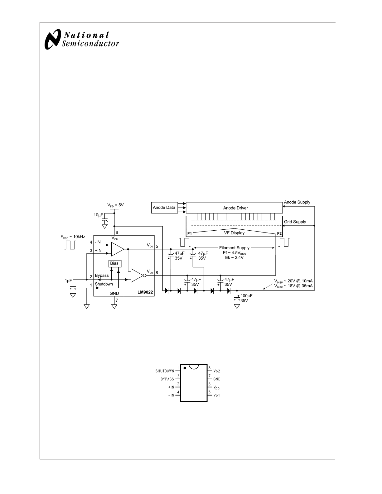
20021501
FIGURE 1. Typical Application Circuit
Connection Diagram
MSOP, Small Outline, and DIP Package
Top View
Order Number LM9022M or LM9022N
See NS Package Number M08A or N08E
© 2005 National Semiconductor Corporation DS200215 www.national.com
20021502
Absolute Maximum Ratings (Note 1)
If Military/Aerospace specified devices are required,
LM9022
please contact the National Semiconductor Sales Office/
Distributors for availability and specifications.
Supply Voltage -0.3V to +6.0V
Supply Temperature −65˚C to +150˚C
Input Voltage −0.3V to V
Power Dissipation (Note 3) Internally Limited
DD
+0.3V
Vapor Phase (60 sec.) 215˚C
Infrared (15 sec.) 220˚C
θ
(typ) —M08A 35˚C/W
JC
θ
(typ) — M08A 140˚C/W
JA
θ
(typ) — N08E 37˚C/W
JC
θ
(typ) — N08E 107˚C/W
JA
Operating Ratings
ESD Susceptibility (Note 4) 5000V
ESD Susceptibility (Note 5) 250V
Junction Temperature 150˚C
Soldering Information
Temperature Range
T
MIN
≤ TA≤ T
MAX
−40˚C ≤ TA≤ 85˚C
Supply Voltage 2.0V ≤ V
Small Outline Package
Electrical Characteristics (Notes 1, 2)
The following specifications apply for V
Limits apply for T
= 25˚C.
A
DD
= 5V, V
PIN3=VPIN2,VSHUTDOWN
Symbol Parameter Conditions
I
DD
Quiescent Power Supply
VIN= 0V, Io= 0A, V
SHUTDOWN
Current
Power Supply Current during
V
SHUTDOWN
=VDD(Note 8) 0.6 2 µA
shutdown
V
BP
V
OUT
Note 1: Absolute Maximum Ratings indicate limits beyond which damage to the device may occur. Operating Ratings indicate conditions for which the device is
functional, but do not guarantee specific performance limits. Electrical Characteristics state DC and AC electrical specifications under particular test conditions which
guarantee specific performance limits. This assumes that the device is within the Operating Ratings. Specifications are not guaranteed for parameters where no limit
is given, however, the typical value is a good indication of device performance.
Note 2: All voltages are measured with respect to the ground pin, unless otherwise specified.
Note 3: The maximum power dissipation must be derated at elevated temperatures and is dictated by T
allowable power dissipation is P
For the θ
Note 4: Human body model, 100pF discharged through a 1.5kΩ resistor.
Note 5: Machine Model, 220pF–240pF discharged through all pins.
Note 6: Typicals are specified at 25˚C and represent the parametric norm.
Note 7: Limits are guaranteed to National’s AOQL (Average Outgoing Quality Level) by design, test, or statistical analysis.
Note 8: Both outputs are high impedance when in shutdown mode.
Bypass Pin Voltage VIN= 0V 2.4 2.5 2.6 V
Output Voltage Across R
=(T
’s for different packages, please see the Application Information section or the Absolute Maximum Ratings section.
JA
DMAX
RL=10Ω 3.6 4.3 V
L
R
=20Ω 4.2 4.6 V
L
)/θJAor the number given in Absolute Maximum Ratings, whichever is lower. For the LM9022, T
JMAX–TA
= 0V, and RL=10Ω unless otherwise specified.
LM9022
Min
(Note 7)
Typical
(Note 6)
Max
(Note 7)
= 0V 6.5 10.0 mA
, θJA, and the ambient temperature TA. The maximum
JMAX
JMAX
DD
≤ 5.5V
Units
= 150˚C.
www.national.com 2
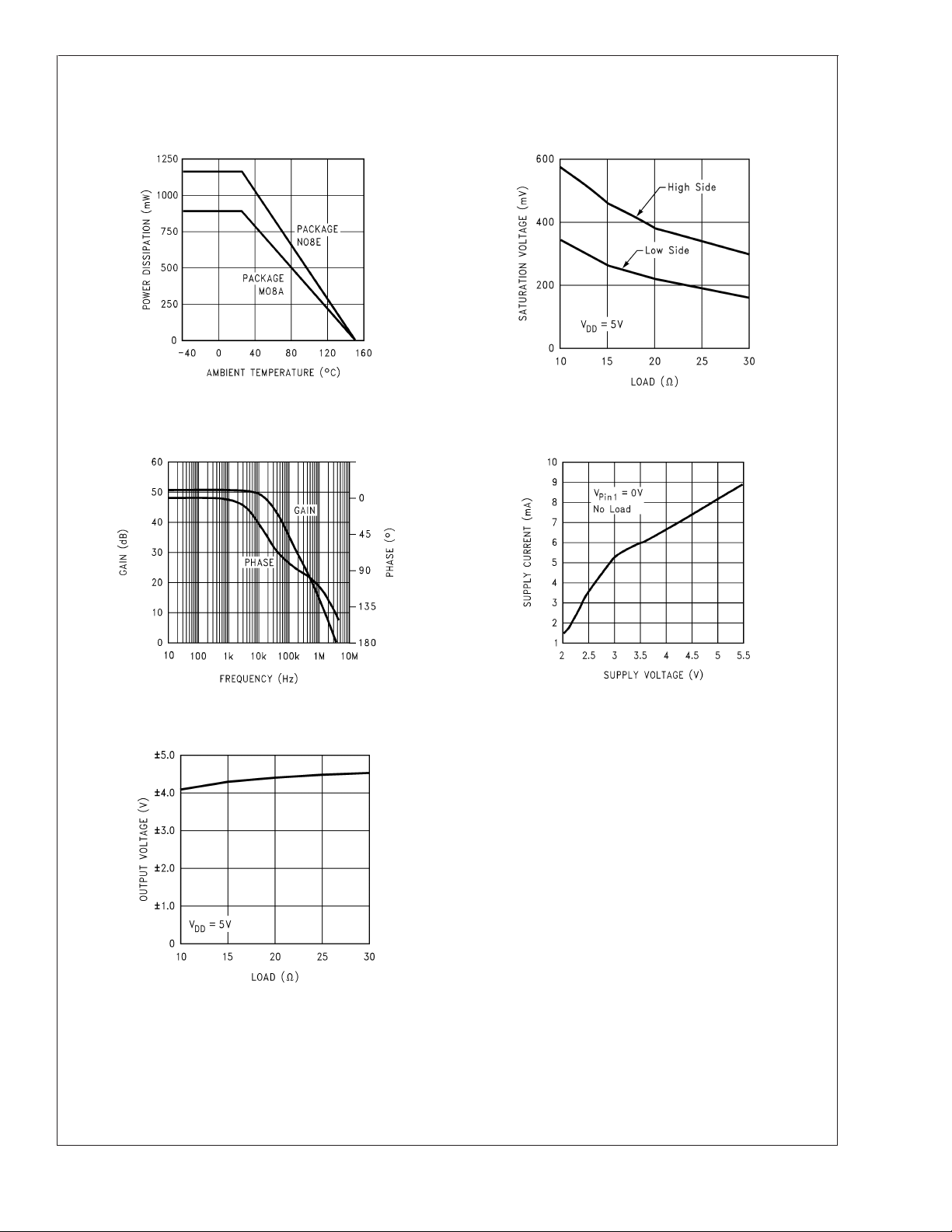
Typical Performance Characteristics
TA= 25˚C, VDD= 5V, unless otherwise specified.
Power Derating Curve Output Saturation Voltage
LM9022
vs Load
Open Loop
Frequency Response
Differential Output Voltage
vs Load
20021514
20021519
20021515
Supply Current
vs Supply Voltage
20021520
20021540
www.national.com3

Application Information
LM9022
LM9022 FUNCTIONALITY
Typically a VFD filament requires a low voltage AC power
source in order to create a constant brightness across its
length. Such a power source is not readily available in a
most systems. Existing implementations show different circuits for supplying an AC power for a VFD filament but they
require an AC power input, or do not have a standby control,
or generate high EMI. The LM9022 can solve all these
problems in one compact circuit.
A DC power supply is employed to power two power operational amplifiers: POA1 and POA2. The first power operational amplifier (POA1) can utilize an external feedback circuit that will cause it self-oscillate. In a second version,
POA1 is driven from an external signal source. The shape of
the output wave delivered by POA1 can be square, sinusoidal, triangular, trapezoidal, clipped sinusoidal or any other
shape, depending on the feedback circuit or the signal
source used. The output of this POA1 is connected externally to one end of the VFD filament, and internally to the
input of a second power operational amplifier: POA2. POA2
is internally configured as an inverting unity gain circuit. The
output of the POA2 is connected to the second end of the
VFD filament. This provides a differential and symmetrical
AC signal to the fila
An external standby control signal applied to the Shutdown
pin can be used to turn of both power operational amplifiers.
BRIDGE CONFIGURATION EXPLANATION
As shown in Figure 1, the LM9022 has two operational
amplifiers internally. Figure 1 shows that the output of amplifier one serves as the input to amplifier two, which results
in both amplifiers producing signals identical in magnitude,
but 180˚ out of phase.
By driving the load differentially through outputs Vo1 and
Vo2, an amplifier configuration commonly referred to as
“bridged mode” is established. Bridged mode operation is
different from the classical single-ended amplifier configuration where one side of its load is connected to ground.
A bridge amplifier design has a few distinct advantages over
the single-ended configuration, as it provides differential
drive to the load, thus doubling output swing for a specified
supply voltage. Four times the output power is possible as
compared to a single-ended amplifier under the same conditions.
POWER DISSIPATION
For the SO package, θ
= 107˚C/W, and for the MSOP package, θJA= 210˚C/W
θ
JA
assuming free air operation. The θ
using some form of heat sinking. The resultant θ
= 140˚C/W, for the DIP package,
JA
can be decreased by
JA
will be the
JA
summation of the θ
case of the package, θ
resistance and θ
, θCS, and θSA. θJCis the junction to
JC
is the case to heat sink thermal
CS
is the heat sink to ambient thermal
SA
resistance. By adding additional copper area around the
LM9022, the θ
can be reduced from its free air value for
JA
the SO package. Depending on the ambient temperature,
, and the θJA, Equation 2 can be used to find the maximum
T
A
internal power dissipation supported by the IC packaging. If
the result of Equation 1 is greater than that of Equation 2,
then either the supply voltage must be decreased, the load
impedance increased, the θ
decreased, or the ambient
JA
temperature reduced. For the typical application of a 5V
power supply, with an 10Ω load, and no additional heatsinking, the maximum ambient temperature possible without
violating the maximum junction temperature is approximately
61˚C provided that device operation is around the maximum
power dissipation point and assuming surface mount packaging.
POWER SUPPLY PIN
As with any power device, proper supply bypassing is critical
for low noise performance. Typical applications will require
both a 22µf electrolyte and a 0.1µF ceramic capacitor to
bypass the supply pin to ground. These capacitors should be
as close to the LM9022 as is physically possible, and are in
addition to any capacitors that may be needed for regulator
stability.
BYPASS PIN
The internal bias circuit (Fig 1) generates an internal reference voltage that is typically equal to one half of V
DD
. This
voltage is available at the bypass pin and is applied directly
to the non-inverting input of the inverting driver. Typical
applications will require a bypass capacitor in the range of
0.1µF to 1µF to bypass the supply pin to ground. This
capacitor should be as close to the LM9022 as is physically
possible.
SHUTDOWN FUNCTION
In order to reduce power consumption while not in use, the
LM9022 contains a shutdown pin to externally turn off the
amplifier’s bias circuitry. This shutdown feature turns the
amplifier off when a logic high is placed on the shutdown pin.
The trigger point between a logic low and logic high level is
typically half- supply. It is best to switch between ground and
supply to provide maximum device performance. By switching the shutdown pin to V
, the LM9022 supply current
DD
draw will be minimized in idle mode. While the device will be
disabled with shutdown pin voltages less then V
, the idle
DD
current may be greater than the typical value of 0.6µA. In
either case, the shutdown pin should be tied to a definite
voltage to avoid unwanted state changes.
www.national.com 4

Application Information (Continued)
FIGURE 2. Filament Supply using External Oscillator
LM9022
20021544
FIGURE 3. Filament Supply using Self Oscillation
20021545
www.national.com5

Physical Dimensions inches (millimeters) unless otherwise noted
LM9022
Order Number LM9022M
NS Package Number M08A
Order Number LM9022N
NS Package Number N08E
www.national.com 6

Notes
LM9022 Vacuum Fluorescent Display Filament Driver
National does not assume any responsibility for use of any circuitry described, no circuit patent licenses are implied and National reserves
the right at any time without notice to change said circuitry and specifications.
For the most current product information visit us at www.national.com.
LIFE SUPPORT POLICY
NATIONAL’S PRODUCTS ARE NOT AUTHORIZED FOR USE AS CRITICAL COMPONENTS IN LIFE SUPPORT DEVICES OR SYSTEMS
WITHOUT THE EXPRESS WRITTEN APPROVAL OF THE PRESIDENT AND GENERAL COUNSEL OF NATIONAL SEMICONDUCTOR
CORPORATION. As used herein:
1. Life support devices or systems are devices or systems
which, (a) are intended for surgical implant into the body, or
(b) support or sustain life, and whose failure to perform when
properly used in accordance with instructions for use
2. A critical component is any component of a life support
device or system whose failure to perform can be reasonably
expected to cause the failure of the life support device or
system, or to affect its safety or effectiveness.
provided in the labeling, can be reasonably expected to result
in a significant injury to the user.
BANNED SUBSTANCE COMPLIANCE
National Semiconductor manufactures products and uses packing materials that meet the provisions of the Customer Products
Stewardship Specification (CSP-9-111C2) and the Banned Substances and Materials of Interest Specification (CSP-9-111S2) and contain
no ‘‘Banned Substances’’ as defined in CSP-9-111S2.
Leadfree products are RoHS compliant.
National Semiconductor
Americas Customer
Support Center
Email: new.feedback@nsc.com
Tel: 1-800-272-9959
www.national.com
National Semiconductor
Europe Customer Support Center
Fax: +49 (0) 180-530 85 86
Email: europe.support@nsc.com
Deutsch Tel: +49 (0) 69 9508 6208
English Tel: +44 (0) 870 24 0 2171
Français Tel: +33 (0) 1 41 91 8790
National Semiconductor
Asia Pacific Customer
Support Center
Email: ap.support@nsc.com
National Semiconductor
Japan Customer Support Center
Fax: 81-3-5639-7507
Email: jpn.feedback@nsc.com
Tel: 81-3-5639-7560
 Loading...