

查询LM760供应商
LM760
High Speed Differential Comparator
LM760 High Speed Differential Comparator
December 1994
General Description
The LM760 is a differential voltage comparator offering considerable speed improvement over the LM710 family and
operates from symmetric supplies of
LM760 can be used in high speed analog-to-digital conversion systems and as a zero crossing detector in disc file and
tape amplifiers. The LM760 output features balanced rise
and fall times for minimum skew and close matching between the complementary outputs. The outputs are TTL
compatible with a minimum sink capability of two gate loads.
g
4.5V tog6.5V. The
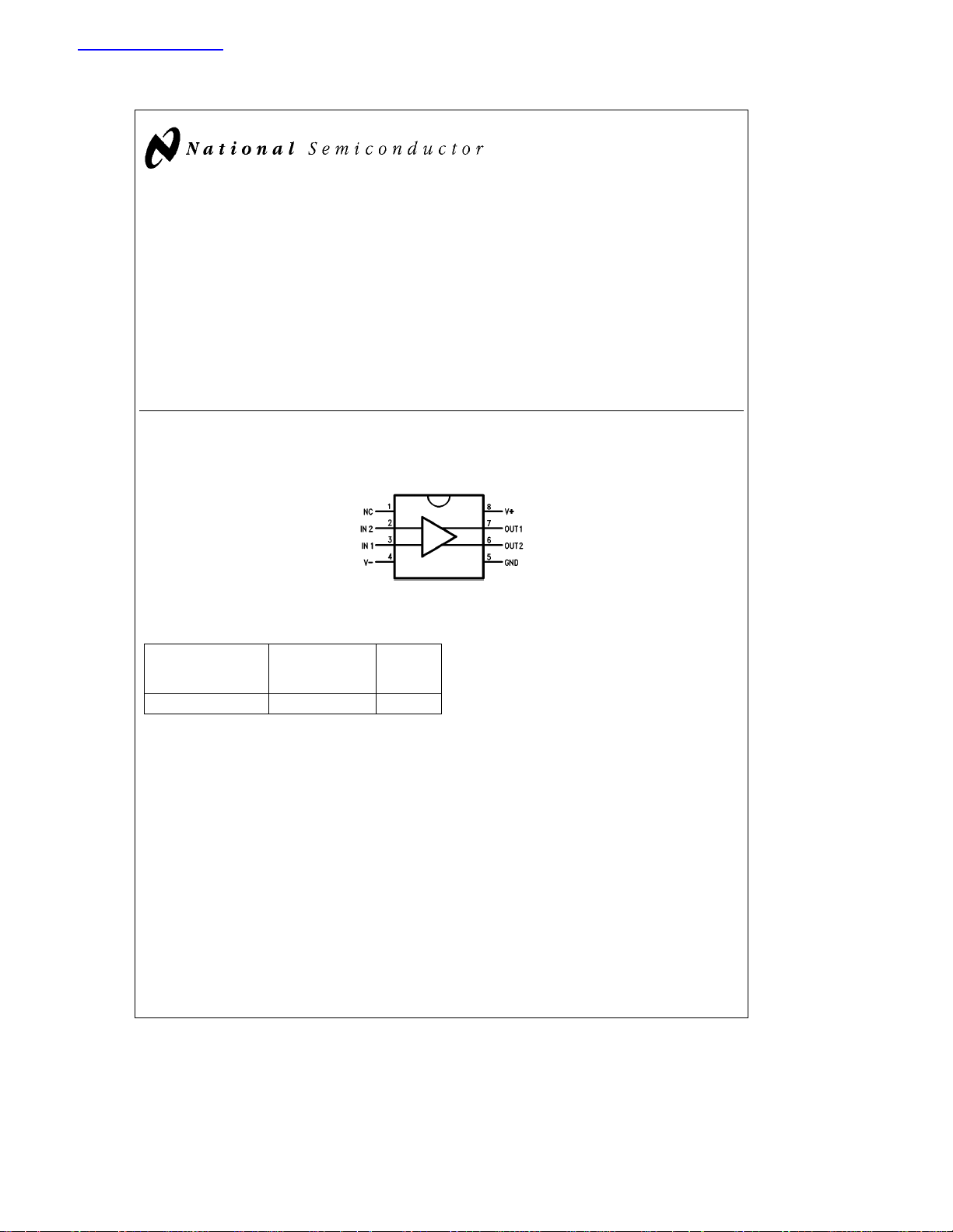
Connection Diagram
8-Lead DIP
Top View
Ordering Information
Temperature Range NSC
Commercial Package Type Package
0
Ctoa70§C Drawing
§
LM760CN 8-lead Plastic DIP N08E
Features
Y
Guaranteed high speedÐ 25 ns response time
Y
Guaranteed delay matching on both outputs
Y
Complementary TTL compatible outputs
Y
High sensitivity
Y
Standard supply voltages
Applications
Y
High speed A-to-D
Y
Peak or zero detector
TL/H/10067– 3
C
1995 National Semiconductor Corporation RRD-B30M115/Printed in U. S. A.
TL/H/10067
Absolute Maximum Ratings
If Military/Aerospace specified devices are required,
please contact the National Semiconductor Sales
Office/Distributors for availability and specifications.
Storage Temperature Range
Metal Can and Ceramic DIP
Molded DIP
Operating Temperature Range
Military (LM760)
Commercial (LM760C) 0
b
65§Ctoa175§C
b
65§Ctoa150§C
b
55§Ctoa125§C
Ctoa70§C
§
Lead Temperature
Metal Can and Ceramic DIP
(Soldering, 60 sec.) 300
Molded DIP (Soldering, 10 sec.) 265
Positive Supply Voltage
Negative Supply Voltage
Peak Output Current 10 mA
Differential Input Voltage
Input Voltage V
ESD Susceptibility TBD
C
§
C
§
a
8.0V
b
8.0V
g
5.0V
a
t
t
V
I
LM760
Electrical Characteristics
e
g
V
CC
4.5V tog6.5V, T
Symbol Parameter Conditions Min Typ Max Units
V
IO
I
IO
I
IB
R
O
t
PD
Dt
PD
Input Offset Voltage R
Input Offset Current 0.5 7.5 mA
Input Bias Current 8.0 60 mA
Output Resistance (Either Output) V
Response Time T
Response Time Difference
between Outputs (Note 1)
ofaVI1)b(tPDofbVI2)T
(t
PD
(tPDofaVI2)b(tPDofbVI1)T
(tPDofaVI1)b(tPDofaVI2)T
(tPDofbVI1)b(tPDofbVI2)T
R
I
C
I
DVIO/DT Average Temperature Coefficient R
DIIO/DT Average Temperature Coefficient T
V
IR
V
IDR
V
OH
V
OL
a
I
b
I
Input Resistance fe1.0 MHz 12 kX
Input Capacitance fe1.0 MHz 8.0 pF
of Input Offset Voltage T
of Input Offset Current
Input Voltage Range V
Differential Input Voltage Range
Output Voltage HIGH 0 mAsI
(Either Output) V
Output Voltage LOW I
(Either Output)
Positive Supply Current V
Negative Supply Current V
eb
55§Ctoa125§C, T
A
e
25§C for typical figures, unless otherwise specified
A
s
200X 1.0 6.0 mV
S
e
V
O
OH
e
25§C (Note 3) 18 30
A
e
T
25§C (Note 4) 25 ns
A
100 X
(Note 5) 16
e
25§C 5.0
A
e
25§C 5.0 ns
A
e
25§C 7.5
A
e
25§C 7.5
A
e
50X,
S
eb
55§Ctoa125§C
A
ea
25§Ctoa125§C 2.0
A
ea
25§Ctob55§C 7.0
T
A
e
g
6.5V
CC
s
5.0 mA
OH
ea
5.0V V
CC
e
I
80 mA, V
OH
e
3.2 mA
OL
e
g
CC
e
g
CC
e
g
4.5V 2.4 3.0
CC
6.5V 18 32 mA
6.5V 9.0 16 mA
g
4.0
2.4 3.2
3.0 mV/
g
4.5 V
g
5.0 V
0.25 0.4 V
nA/
b
V
C
§
C
§
2
LM760C
Electrical Characteristics
e
g
V
CC
4.5V tog6.5V, T
Symbol Parameter Conditions Min Typ Max Units
V
IO
I
IO
I
IB
R
O
t
PD
Dt
PD
Input Offset Voltage R
Input Offset Current 0.5 7.5 mA
Input Bias Current 8.0 60 mA
Output Resistance (Either Output) V
Response Time T
Response Time Difference
between Outputs (Note 1)
ofaVI1)b(tPDofbVI2)T
(t
PD
(tPDofaVI2)b(tPDofbVI1)T
(tPDofaVI1)b(tPDofaVI2)T
(tPDofbVI1)b(tPDofbVI2)T
R
I
C
I
DVIO/DT Average Temperature Coefficient R
DIIO/DT Average Temperature Coefficient T
V
IR
V
IDR
V
OH
V
OL
a
I
b
I
Note 1: T
Note 2: Ratings apply to ambient temperature at 25
Note 3: Response time measured from the 50% point of a 30 mV
Note 4: Response time measured from the 50% point of a 2.0 V
Note 5: Response time measured from the start of a 100 mV input step with 5.0 mV overdrive to the time when the output crosses the logic threshold.
Input Resistance fe1.0 MHz 12 kX
Input Capacitance fe1.0 MHz 8.0 pF
of Input Offset Voltage T
of Input Offset Current
Input Voltage Range V
Differential Input Voltage Range
Output Voltage HIGH 0 mAsI
(Either Output) V
Output Voltage LOW I
(Either Output)
Positive Supply Current V
Negative Supply Current V
e
150§C.
J Max
e
0§Ctoa70§C, T
A
e
25§C for typical figures, unless otherwise specified
A
s
200X 1.0 6.0 mV
S
e
V
O
OH
e
25§C (Note 3) 18 30
A
e
T
25§C (Note 4) 25 ns
A
100 X
(Note 5) 16
e
25§C 5.0
A
e
25§C 5.0 ns
A
e
25§C10
A
e
25§C10
A
e
50X,
S
e
0§Ctoa70§C
A
ea
25§Ctoa70§C 5.0
A
ea
25§Cto0§C10
T
A
e
g
6.5V
CC
s
5.0 mA
OH
ea
5.0V V
CC
e
I
80 mA, V
OH
e
3.2 mA
OL
e
g
CC
e
g
CC
C.
§
10 MHz sinusoidal input to the 50% point of the output.
P–P
10 MHz sinusoidal input to the 50% point of the output.
P–P
e
g
4.5V 2.5 3.0
CC
6.5V 18 34 mA
6.5V 9.0 16 mA
g
4.0
2.4 3.2
3.0 mV/
nA/
g
4.5 V
g
5.0 V
0.25 0.4 V
C
§
C
§
3

Typical Performance Characteristics
Response Time for
Various Output Overdrives
Response Time vs
Input Voltage
Voltage Gain vs
Supply Voltage
Response Time for
Various Input Overdrives
Voltage Transfer
Characteristic
Voltage Gain
vs Temperature
Response Time vs
Input Voltage
Voltage Transfer
Characteristic
Input Bias Current
vs Temperature
Input Offset Current
vs Temperature
Response Time
vs Temperature
4
Output Voltage Levels
vs Temperature
TL/H/10067– 5

Typical Performance Characteristics (Continued)
Rise Time vs
Capacitive Load
Equivalent Circuit
Fall Time vs
Capacitive Load
Common Mode Range
vs Supply Voltage
Input Bias Current vs
Differential Input Voltage
TL/H/10067– 6
TL/H/10067– 4
5

Typical Applications (Note 1)
Fast Positive Peak Detector
Level Detector with Hysteresis
Line Receiver with High Common Mode Range
TL/H/10067– 7
TL/H/10067– 8
Common mode range
Differential Input Sensitivity
must be adjusted for optimum common mode rejection.
P
1
e
For R
200X:
S
Common mode range
e
Sensitivity
Zero Crossing Detector (Note 2)
20 mV
R
S
e
c
g
4
V
50
R
S
e
c
5
mV
50
e
g
16V
TL/H/10067– 10
Note 1: Lead numbers shown are for Metal Package only.
Note 2: All resistor values in ohms.
Total delaye30 ns
Input Frequency
Minimum input voltage
e
6
300 Hz to 3.0 MHz
e
20 mV
P–P
TL/H/10067– 9

Typical Applications (Note 1) (Continued)
High Speed 3-Bit A/D Converter
Input voltage rangee3.5V
Typical conversion speed
TL/H/10067– 11
e
30 ns
7

8

Physical Dimensions inches (millimeters)
8-Lead Metal Can Package (H)
Order Number LM760CH or LM760H
NS Package Number H08A
8-Lead Ceramic Dual-In-Line Package (J)
Order Number LM760CJ or LM760J
NS Package Number J08A
9

Physical Dimensions inches (millimeters) (Continued)
LM760 High Speed Differential Comparator
8-Pin Molded Dual-In-Line Package (N)
Order Number LM760CN
NS Package Number N08E
LIFE SUPPORT POLICY
NATIONAL’S PRODUCTS ARE NOT AUTHORIZED FOR USE AS CRITICAL COMPONENTS IN LIFE SUPPORT
DEVICES OR SYSTEMS WITHOUT THE EXPRESS WRITTEN APPROVAL OF THE PRESIDENT OF NATIONAL
SEMICONDUCTOR CORPORATION. As used herein:
1. Life support devices or systems are devices or 2. A critical component is any component of a life
systems which, (a) are intended for surgical implant support device or system whose failure to perform can
into the body, or (b) support or sustain life, and whose be reasonably expected to cause the failure of the life
failure to perform, when properly used in accordance support device or system, or to affect its safety or
with instructions for use provided in the labeling, can effectiveness.
be reasonably expected to result in a significant injury
to the user.
National Semiconductor National Semiconductor National Semiconductor National Semiconductor
Corporation Europe Hong Kong Ltd. Japan Ltd.
1111 West Bardin Road Fax: (
Arlington, TX 76017 Email: cnjwge@tevm2.nsc.com Ocean Centre, 5 Canton Rd. Fax: 81-043-299-2408
Tel: 1(800) 272-9959 Deutsch Tel: (
Fax: 1(800) 737-7018 English Tel: (
National does not assume any responsibility for use of any circuitry described, no circuit patent licenses are implied and National reserves the right at any time without notice to change said circuitry and specifications.
Fran3ais Tel: (
Italiano Tel: (
a
49) 0-180-530 85 86 13th Floor, Straight Block, Tel: 81-043-299-2309
a
49) 0-180-530 85 85 Tsimshatsui, Kowloon
a
49) 0-180-532 78 32 Hong Kong
a
49) 0-180-532 93 58 Tel: (852) 2737-1600
a
49) 0-180-534 16 80 Fax: (852) 2736-9960
 Loading...