

LM6588
TFT-LCD Quad, 16V RRIO High Output Current
Operational Amplifier
LM6588 TFT-LCD Quad, 16V RRIO High Output Current Operational Amplifier
July 2005
General Description
The LM6588 is a low power, high voltage, rail-to-rail inputoutput amplifier ideally suited for LCD panel V
gamma buffer applications. The LM6588 contains four unity
gain stable amplifiers in one package. It provides a common
mode input ability of 0.5V beyond the supply rails, as well as
an output voltage range that extends to within 50mV of either
supply rail. With these capabilities, the LM6588 provides
maximum dynamic range at any supply voltage. Operating
on supplies ranging from 5V to 16V, while consuming only
750µA per amplifier, the LM6588 has a bandwidth of 24MHz
(−3dB).
The LM6588 also features fast slewing and settling times,
along with a high continuous output capability of 75mA. This
output stage is capable of delivering approximately 200mA
peak currents in order to charge or discharge capacitive
loads. These features are ideal for use in TFT-LCDs.
The LM6588 is available in the industry standard 14-pin SO
package and in the space-saving 14-pin TSSOP package.
The amplifiers are specified for operation over the full −40˚C
to +85˚C temperature range.
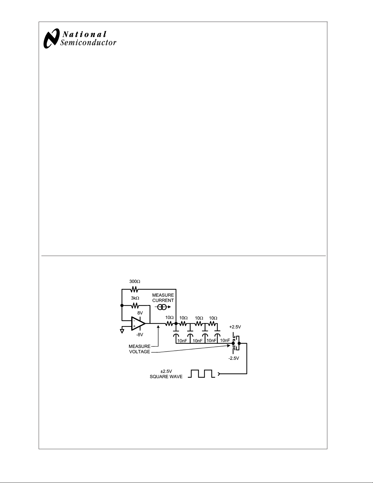
COM
driver and
Test Circuit Diagram
Features
(VS=5V,TA= 25˚C typical values unless specified)
n Input common mode voltage 0.5V beyond rails
n Output voltage swing (R
n Output short circuit current
n Continuous output current 75mA
n Supply current (per amp, no load) 750µA
n Supply voltage range 5V to 16V
n Unity gain stable
n −3dB bandwidth (A
n Slew rate 11V/µSec
n Settling time 270ns
n SO-14 and TSSOP-14 package
n Manufactured in National Semiconductor’s
state-of-the-art bonded wafer, trench isolated
complementary bipolar VIP10
performance at low power levels
=2kΩ) 50mV from rails
L
= +1) 24MHz
V
™
technology for high
±
200mA
Applications
n LCD panel V
n LCD panel gamma buffer
n LCD panel repair amp
COM
driver
20073401
© 2005 National Semiconductor Corporation DS200734 www.national.com

Absolute Maximum Ratings (Note 1)
If Military/Aerospace specified devices are required,
LM6588
please contact the National Semiconductor Sales Office/
Input Common Mode Voltage V
Junction Temperature (Note 4) 150˚C
Distributors for availability and specifications.
Operating Ratings (Note 1)
ESD Tolerance (Note 2)
Human Body Model 2.5KV
Machine Model 250V
+-V−
Supply Voltage (V
Differential Input Voltage
) 18V
±
5.5V
Output Short Circuit to Ground (Note 3) Continuous
Storage Temperature Range −65˚C to 150˚C
Supply Voltage 4V ≤ V
Temperature Range −40˚C to +85˚C
Thermal Resistance (θ
)
JA
SOIC-14 145˚C/W
TSSOP-14 155˚C/W
16V DC Electrical Characteristics (Note 13)
Unless otherwise specified, all limits guaranteed for at TJ= 25˚C, VCM=1⁄2VSand RL=2kΩ. Boldface limits apply at the tem-
perature extremes.
Symbol Parameter Conditions Min
(Note 6)
V
OS
TC V
Input Offset Voltage 0.7 4
Input Offset Voltage Average
OS
Drift
I
B
I
OS
R
IN
Input Bias Current −0.3/+0.3
Input Offset Current 16 150
Input Resistance Common Mode 20
Differential Mode 0.5
CMRR Common Mode Rejection
V
= 0 to +16V 75
CM
Ratio
= 0 to 14.5V 78
V
CM
PSRR Power Supply Rejection Ratio V
CMVR Input Common-Mode Voltage
=±1V 80
CM
>
CMRR
50dB
Range
A
V
Large Signal Voltage Gain
RL=2kΩ,VO= 0.5 to +15.5V 80
(Note 7)
V
I
SC
I
CONT
I
S
O
Output Swing High RL=2kΩ 15.8
Output Swing Low R
Output Short Circuit Current
(Note 11)
Continuous Output Current
(Note 12)
=2kΩ 0.100 0.200
L
Sourcing 170 230
Sinking 170 230
Sourcing 40
Sinking 40
Supply Current (per Amp) 800 1200
70
72
75
16.2
75
15.6
Typ
(Note 5)
Max
(Note 6)
6
5
±
1
±
7
300
103
103
103 dB
0
−0.2 V
16
108 dB
15.9
1500
−
≤ 16V
S
Units
mV
µV/˚C
µA
nA
MΩ
dB
V
mA
mA
µA
to V
+
16V AC Electrical Characteristics (Note 13)
Unless otherwise specified, all limits guaranteed for at TJ= 25˚C, VCM=1⁄2VSand RL=2kΩ. Boldface limits apply at the tem-
perature extremes.
Symbol Parameter Conditions Min
SR Slew Rate (Note 9) A
www.national.com 2
= +1, VIN= 10V
V
PP
(Note 6)
8 15 V/µs
Typ
(Note 5)
Max
(Note 6)
Units

16V AC Electrical Characteristics (Note 13) (Continued)
Unless otherwise specified, all limits guaranteed for at TJ= 25˚C, VCM=1⁄2VSand RL=2kΩ. Boldface limits apply at the tem-
perature extremes.
Symbol Parameter Conditions Min
(Note 6)
Typ
(Note 5)
Max
(Note 6)
Units
Unity Gain Bandwidth Product 15.4 MHz
−3dB Frequency A
Φ
m
t
s
t
p
HD2 2
Phase Margin 61 deg
Settling Time (0.1%) AV= −1, AO=±5V, RL= 500Ω 780 ns
Propagation Delay AV= −2, VIN=±5V, RL= 500Ω 20 ns
nd
Harmonic Distortion
= 1MHz (Note 10)
F
IN
HD3 3rd Harmonic Distortion
= 1MHz (Note 10)
F
IN
e
n
Input-Referred Voltage Noise f = 10kHz 23 nV/
= +1 10 24 MHz
V
V
=2V
OUT
V
OUT
=2V
PP
PP
−53 dBc
−40 dBc
5V DC Electrical Characteristics (Note 13)
Unless otherwise specified, all limits guaranteed for at TJ= 25˚C, VCM=1⁄2VSand RL=2kΩ. Boldface limits apply at the tem-
perature extremes.
Symbol Parameter Conditions Min
(Note 6)
V
OS
TC V
Input Offset Voltage 0.7 4
Input Offset Voltage Average
OS
Drift
I
B
I
OS
R
IN
Input Bias Current −0.3/+0.3
Input Offset Current 20 150
Input Resistance Common Mode 20
Differential Mode 0.5
CMRR Common Mode Rejection
V
Stepped from 0 to 5V 70
CM
Ratio
VCMStepped from 0 to 3.5V 75
PSRR Power Supply Rejection Ratio V
CMVR Input Common-Mode Voltage
S=VCC
CMRR
= 3.5V to 5.5V 80
>
50dB
Range
A
V
Large Signal Voltage Gain
RL=2kΩ,VO= 0 to 5V 80
(Note 7)
V
O
Output Swing High RL=2kΩ 4.85
Output Swing Low RL=2kΩ 0.05 0.15
I
SC
I
CONT
I
S
Output Short Circuit Current
(Note 11)
Continuous Output Current
(Note 12)
Sourcing 160 200
Sinking 160 200
Sourcing 75
Sinking 75
Supply Current (per Amp) 750 1000
66
70
75
5.2
75
4.7
Typ
(Note 5)
Max
(Note 6)
6
10
±
1
±
7
300
105
105
92
0.0
−0.2 V
5.0
106 dB
4.95
1250
Units
µV/˚C
LM6588
mV
µA
nA
MΩ
dB
dB
V
mA
mA
µA
www.national.com3
5V AC Electrical Characteristics (Note 13)
Unless otherwise specified, all limits guaranteed for at TJ= 25˚C, VCM=1⁄2VSand RL=2kΩ. Boldface limits apply at the tem-
LM6588
perature extremes.
Symbol Parameter Conditions Min
(Note 6)
SR Slew Rate (Note 9) A
= +1, VIN= 3.5V
V
PP
Unity Gain Bandwidth Product 15.3 MHz
−3dB Frequency A
Φ
m
t
s
t
p
HD2 2
Phase Margin 56 deg
Settling Time (0.1%) AV= −1, VO=±1V, RL= 500Ω 270 ns
Propagation Delay AV= −2, VIN=±1V, RL= 500Ω 21 ns
nd
Harmonic Distortion
= 1MHz (Note 10)
F
IN
HD3 3rd Harmonic Distortion
= 1MHz (Note 10)
F
IN
e
n
Note 1: Note 1: Absolute maximum Ratings indicate limits beyond which damage to the device may occur. Operating Ratings indicate conditions for which the
device is intended to be functional, but specific performance is not guaranteed. For guaranteed specifications and the test conditions, see the Electrical
Characteristics.
Note 2: For testing purposes, ESD was applied using human body model, 1.5kΩ in series with 100pF.
Note 3: Applies to both single-supply and split-supply operation. Continuous short circuit operation at elevated ambient temperature can result in exceeding the
maximum allowed junction temperature of 150˚C
Note 4: The maximum power dissipation is a function of T
P
D
Note 5: Typical values represent the most likely parametric norm.
Note 6: All limits are guaranteed by testing or statistical analysis.
Note 7: Large signal voltage gain is the total output swing divided by the input signal required to produce that swing.
Note 8: The open loop output current is guaranteed, by the measurement of the open loop output voltage swing.
Note 9: Slew rate is the average of the raising and falling slew rates.
Note 10: Harmonics are measured with A
Note 11: Continuous operation at these output currents will exceed the power dissipation ability of the device
Note 12: Power dissipation limits may be exceeded if all four amplifiers source or sink 40mA. Voltage across the output transistors and their output currents must
be taken into account to determine the power dissipation of the device
Note 13: Electrical table values apply only for factory testing conditions at the temperature indicated. Factory testing conditions result in very limited self-heating of
the device such that T
See applications section for information on temperature de-rating of this device.
Input-Referred Voltage Noise f = 10kHz 23 nV/
=(T
J(MAX)-TA
)/ θJA. All numbers apply for packages soldered directly onto a PC board.
= +2 and RL= 100Ω and VIN=1VPPto give V
V
. No guarantee of parametric performance is indicated in the electrical tables under conditions of internal self heating where T
J=TA
= +1 10 24 MHz
V
V
=2V
OUT
V
OUT
PP
=2V
PP
, θJA, and TA. The maximum allowable power dissipation at any ambient temperature is
J(MAX)
=2VPP.
OUT
Typ
(Note 5)
Max
(Note 6)
11 V/µs
−53 dBc
−40 dBc
Units
>
J
TA.
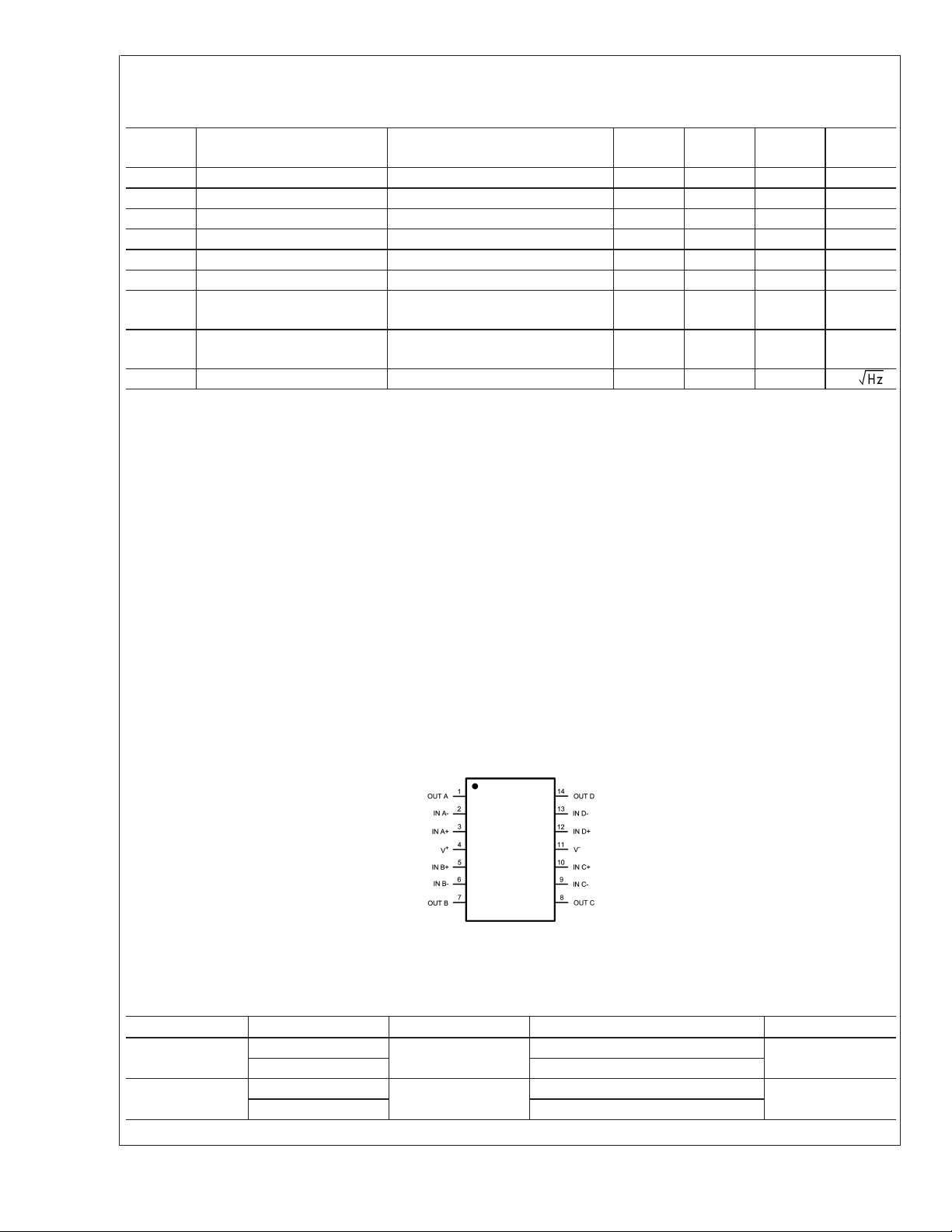
Connection Diagram
14-Pin SOIC/TSSOP
Top View
20073402
Ordering Information
Package Part Number Package Marking Transport Media NSC Drawing
14-Pin SOIC
14-Pin TSSOP
www.national.com 4
LM6588MA
LM6588MAX 2.5k Units Tape and Reel
LM6588MT
LM6588MTX 2.5k Units Tape and Reel
LM6588MA
LM6588MT
95 Units/Rail
95 Units/Rail
M14A
MTC14
LM6588
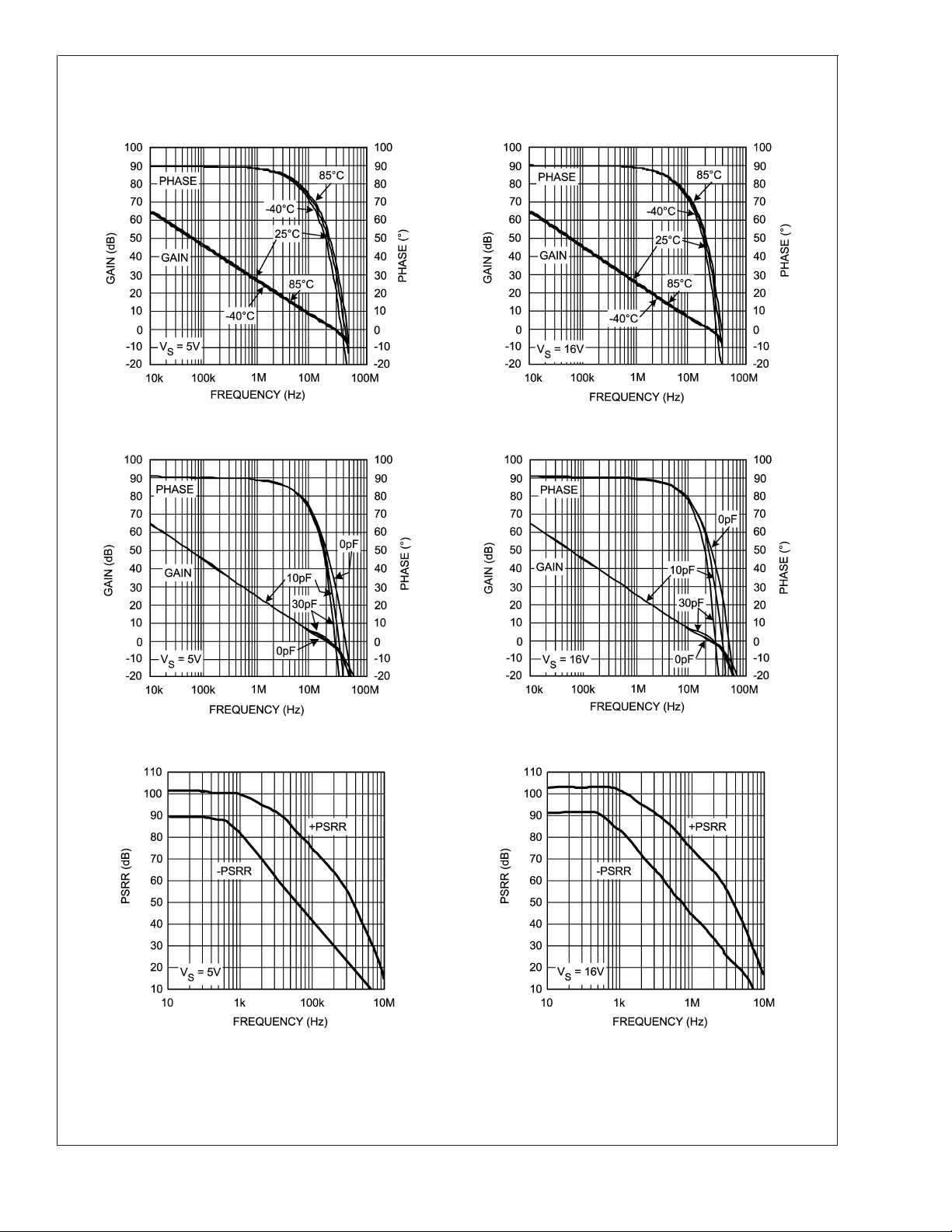
Typical Performance Characteristics Unless otherwise specified, all limits guaranteed for T
= 1/2VSand RL=2kΩ.
V
CM
Gain Phase vs. Temperature (V
Gain Phase vs. Capacitive Loading (VS= 5V) Gain Phase vs. Capacitive Loading (VS= 16V)
= 5V) Gain Phase vs. Temperature (VS= 16V)
S
20073403
= 25˚C,
J
20073404
20073405
PSRR (VS= 5V) PSRR (VS= 16V)
20073407 20073408
20073406
www.national.com5

Typical Performance Characteristics Unless otherwise specified, all limits guaranteed for T
= 1/2VSand RL=2kΩ. (Continued)
V
CM
LM6588
CMRR (V
Settling Time vs. Input Step Amplitude
(Output Slew and Settle Time)
= 5V) CMRR (VS= 16V)
S
20073409 20073410
Settling Time vs. Capacitive Loading
(Output Slew and Settle Time)
= 25˚C,
J
20073411
Crosstalk Rejection vs. Frequency
(Output to Output) Input Voltage Noise vs. Frequency
20073413
www.national.com 6
20073412
20073414

LM6588
Typical Performance Characteristics Unless otherwise specified, all limits guaranteed for T
= 1/2VSand RL=2kΩ. (Continued)
V
CM
Stability vs. Capacitive Load Unity Gain (V
Small Signal Step Response Small Signal Step Response
= 16V) Large Signal Step Response
S
20073415
20073416
= 25˚C,
J
20073417 20073418
Closed Loop Output Impedance vs. Frequency (AV= +1) I
20073419
vs. Common Mode Voltage (VS=±5V)
SUPPLY
20073420
www.national.com7

Typical Performance Characteristics Unless otherwise specified, all limits guaranteed for T
= 1/2VSand RL=2kΩ. (Continued)
V
CM
LM6588
V
vs. Common Mode Voltage (VS= 16V) VOSvs. V
OS
(Typical Unit), (VS= 10V)
OUT
= 25˚C,
J
V
OUT
I
SUPPLY
from V+vs. I
SOURCE
vs. Supply Voltage
20073421
V
from V−vs. I
OUT
20073423 20073424
SINK
20073422
20073425
www.national.com 8

Application Notes
CIRCUIT DESCRIPTION GENERAL & SPEC
The LM6588 is a bipolar process operational amplifier. It has
an exceptional output current capability of 200mA. The part
has both rail to rail inputs and outputs. It has a −3dB bandwidth of 24MHz. The part has input voltage noise of 23nV/
, and 2ndand 3rdharmonic distortion of −53dB and
−40dB respectively.
INPUT SECTION
The LM6588 has rail to rail inputs and thus has an input
range over which the device may be biased of V
0.5V, and V
+
plus 0.5V. The ultimate limit on input voltage
excursion is the ESD protection diodes on the input pins.
The most important consideration in Rail-to-Rail input op
amps is to understand the input structure. Most Rail-to-Rail
input amps use two differential input pairs to achieve this
function. This is how the LM6588 works. A conventional PNP
differential transistor pair provides the input gain from 0.5V
below the negative rail to about one volt below the positive
rail. At this point internal circuitry activates a differential NPN
transistor pair that allows the part to function from 1 volt
below the positive rail to 0.5V above the positive rail. The
effect on the inputs pins is as if there were two different op
amps connected to the inputs. This has several unique
implications.
The input offset voltage will change, sometimes from
•
positive to negative as the inputs transition between the
two stages at about a volt below the positive rail. this
effect is seen in the V
vs. VCMchart in the Typical
OS
Performance Characteristics section of this datasheet.
The input bias currents can be either positive or negative.
•
Do not expect a consistent flow in or out of the pins.
The part will have different specifications depending on
•
whether the NPN or PNP stage is operating.
There is a little more input capacitance then a single
•
stage input although the ESD diodes often swamp out the
added base capacitance.
Since the input offset voltages can change from positive
•
to negative the output may not be monotonic when the
inputs are transitioning between the two stages and the
part is in a high gain configuration.
It should be remembered that swinging the inputs across the
input stage transition may cause output distortion and accuracy anomalies. It is also worth noting that anytime any amps
inputs are swung near the rails THD and other specs are
sure to suffer.
OUTPUT SECTION
Current Rating
The LM6588 has an output current rating, sinking or sourcing, of 200mA. The LM6588 is ideally suited to loads that
require a high value of peak current but only a reduced value
of average current. This condition is typical of driving the
gate of a MOSFET. While the output drive rating is 200mA
peak, and the output structure supports rail-to-rail operation,
the attainable output current is reduced when the gain and
drive conditions are such that the output voltage approaches
either rail.
−
minus
Output Power
Because of the increased output drive capability, internal
heat dissipation must be held to a level that does not increase the junction temperature above its maximum rated
value of 150˚ C.
Power Requirements
+
±
and
2.5V
The LM6588 operates from a voltage supply, of V
ground, or from a V
−
and V+split supply. Single-ended
voltage range is +5V to +16V and split supply range is
±
8.0V.
to
APPLICATION HINTS POWER SUPPLIES
Sequencing
Best practice design technique for operational amplifiers
includes careful attention to power sequencing. Although the
LM6588 is a bipolar op amp, recommended op amp turn on
power sequencing of ground (or V
−
), followed by V+, followed by input signal should be observed. Turn off power
sequence should be the reverse of the turn-on sequence.
Depending on how the amp is biased the outputs may swing
to the rails on power-on or power-off. Due to the high output
currents and rail to rail output stage in the LM6588 the output
may oscillate very slightly if the power is slowly raised between 2V and 4V The part is unconditionally stable at 5V.
Quick turn-off and turn-on times will eliminate oscillation
problems.
PSRR and Noise
Care should be taken to minimize the noise in the power
supply rails. The figure of merit for an op amp’s ability to
keep power supply noise out of the signal is called Power
Supply Rejection Ratio (PSRR). Observe from the PSRR
charts in the Typical Performance Characteristics section
that the PSRR falls of dramatically as the frequency of the
noise on the power supply line goes up. This is one of the
reasons switching power supplies can cause problems. It
should also be noticed from the charts that the negative
supply pin is far more susceptible to power noise. The design engineer should determine the switching frequencies
and ripple voltages of the power supplies in the system. If
required, a series resistor or in the case of a high current op
amp like the LM6588, a series inductor can be used to filter
out the noise.
Transients
In addition to the ripple and noise on the power supplies
there are also transient voltage changes. This can be
caused by another device on the same power supply suddenly drawing current or suddenly stopping a current draw.
The design engineer should insure that there are no damaging transients induced on the power supply lines when the op
amp suddenly changes current delivery.
LAYOUT
Ground Planes
Do not assume the ground (or more properly, the common or
return) of the power supply is an ocean of zero impedance.
The thinner the trace, the higher the resistance. Thin traces
cause tiny inductances in the power lines. These can react
against the large currents the LM6588 is capable of delivering to cause oscillations, instability, overshoot and distortion.
A ground plane is the most effective way of insuring the
LM6588
www.national.com9

Application Notes (Continued)
ground is a uniform low impedance. If a four layer board
LM6588
cannot be used, consider pouring a plane on one side of a
two layer board. If this cannot be done be sure to use as
wide a trace as practicable and use extra decoupling capacitors to minimize the AC variations on the ground rail.
Decoupling
A high-speed, high-current amp like the LM6588 must have
generous decoupling capacitors. They should be as close to
the power pins as possible. Putting them on the back side
opposite the power pins may give the tightest layout. If
ground and power planes are available, the placement of the
decoupling caps are not as critical.
Breadboards
The high currents and high frequencies the LM6588 operates at, as well as thermal considerations, require that prototyping of the design be done on a circuit board as opposed
to a “Proto-Board” style breadboard.
STABILITY
General:
High speed parts with large output current capability require
special care to insure lack of oscillations. Keep the ”+” pin
isolated from the output to insure stability. As noted above
care should be take to insure the large output currents do not
appear in the ground or ground plane and then get coupled
into the “+” pin. As always, good tight layout is essential as is
adequate use of decoupling capacitors on the power supplies.
Unity Gain
The unity gain or voltage-follower configuration is the most
subject to oscillation. If a part is stable at unity gain it is
almost certain to work in other configurations. In certain
applications where the part is setting a reference voltage or
is being used as a buffer greater stability can be achieved by
configuring the part as a gain of −1 or −2 or +2.
Phase Margin
The phase margin of an op amps gain-phase plot is an
indication of the stability of the amp. It is desirable to have at
least 45˚C of phase margin to insure stability in all cases.
The LM6588 has 60˚C of phase margin even with it’s large
output currents and Rail-to-Rail output stage, which are
generally more prone to stability issues.
Capacitive Load
The LM6588 can withstand 30pF of capacitive load in a unity
gain configuration before stability issues arise. At very large
capacitances, the load capacitor will attenuate the gain like
any other heavy load and the part becomes stable again.
The LM6588 will be stable at 330nF and higher load capacitance. Refer to the chart in the Typical Performance Characteristics section.
OUTPUT
Swing vs. Current
The LM6588 will get to about 25mV or 30mV of either rail
when there is no load. The LM6588 can sink or source
hundreds of milliamperes while remaining less then 0.5V
away from the rail. It should be noted that if the outputs are
driven to the rail and the part can no longer maintain the
feedback loop, the internal circuitry will deliver large base
currents into the huge output transistors, trying to get the
outputs to get past the saturation voltage. The base currents
will approach 16 milliamperes and this will appear as an
increase in power supply current. Operating at this power
dissipation level for extended periods will damage the part,
especially in the higher thermal resistance TSSOP package.
Because of this phenomenon, unused parts should not have
the inputs strapped to either rail, but should have the inputs
biased at the midpoint or at least a diode drop (0.6V) within
the rails.
Self Heating
As discussed above the LM6588 is capable of significant
power by virtue of its 200mA current handling capability. A
TSSOP package cannot sustain these power levels for more
then a brief period.
TFT Display Application
INTRODUCTION
In today’s high-resolution TFT displays, op amps are used
for the following three functions:
1. V
2. Gamma Buffer
3. Panel Repair Buffer
All of these functions utilize op amps as non-inverting, unity-
gain buffers. The V
that supply a well regulated DC voltage. A Panel Repair
Buffer, on the other hand, provides a high frequency signal
that contains part of the display’s visual image.
In an effort to reduce production costs, display manufacturers use a minimum variety of different parts in their TFT
displays. As a result, the same type of op amp will be used
for the V
To perform all these functions, such an op amp must have
the following characteristics:
1. Large output current drive
2. Rail to rail input common mode range
3. Rail to rail output swing
4. Medium speed gain bandwidth and slew rate
The LM6588 meets these requirements. It has a rail-to-rail
input and output, typical gain bandwidth and slew rate of
15MHz and 15V/µs, and it can supply up to 200mA of output
current. The following sections will describe the operation of
V
COM
showing how the LM6588 is well suited for each of these
functions.
BRIEF OVERVIEW OF TFT DISPLAY
To better understand these op amp applications, let’s first
review a few basic concepts of how a TFT display operates.
Figure 1 is a simplified illustration of an LCD pixel. The top
and bottom plates of each pixel consist of Indium-Tin oxide
(ITO), which is a transparent, electrically conductive material. ITO lies on the inner surfaces of two glass substrates
that are the front and back glass panels of a TFT display.
Sandwiched between the two ITO plates is an insulating
material (liquid crystal) that alters the polarization of light to a
lesser a greater amount, depending on how much voltage
(V
PIXEL
placed on the outer surfaces of the two glass substrates,
which in combination with the liquid crystal create a variable
Driver
COM
Driver and Gamma Buffer are buffers
COM
Driver, Gamma Buffer, and Panel Repair Buffer.
COM
Drivers, Gamma Buffers, and Panel Repair Buffers,
) is applied across the two plates. Polarizers are
www.national.com 10

TFT Display Application (Continued)
light filter that modulates light transmitted from the back to
the front of a display. A pixel’s bottom plate lies on the
backside of a display where a light source is applied, and the
top plate lies on the front, facing the viewer. On a Twisted
Neumatic (TN) display, which is typical of most TFT displays,
a pixel transmits the greatest amount of light when V
±
0.5V, and it becomes less transparent as this voltage
less
increases with either a positive or negative polarity. In short,
an LCD pixel can be thought of as a capacitor, through
which, a controlled amount of light is transmitted by varying
.
V
PIXEL
FIGURE 1. Individual LCD Pixel
PIXEL
20073426
LM6588
the Column Drivers supply this voltage via the column lines.
Column Drivers ‘write’ this voltage to the pixels one row at a
time, and this is accomplished by having the Row Drivers
select an individual row of pixels when their voltage levels
are transmitted by the Column Drivers. The Row Drivers
sequentially apply a large positive pulse (typically 25V to
35V) to each row line. This turns-on NMOS transistors con-
is
nected to an individual row, allowing voltages from the column lines to be transmitted to the pixels.
V
DRIVER
COM
The V
driver supplies a common voltage (V
COM
the pixels in a TFT panel. V
is a constant DC voltage that
COM
COM
)toall
lies in the middle of the column drivers’ output voltage range.
As a result, when the column drivers write to a row of pixels,
they apply voltages that are either positive or negative with
respect to V
. In fact, the polarity of a pixel is reversed
COM
each time its row is selected. This allows the column drivers
to apply an alternating voltage to the pixels rather than a DC
signal, which can ‘burn’ a pattern into an LCD display.
When column drivers write to the pixels, current pulses are
injected onto the V
ing stray capacitance between V
line. These pulses result from charg-
COM
and the column lines
COM
(see Figure 2), which ranges typically from 16pF to 33pF per
column. Pixel capacitance contributes very little to these
pulses because only one pixel at a time is connected to a
column, and the capacitance of a single pixel is on the order
of only 0.5pF. Each column line has a significant amount of
series resistance (typically 2kΩ to 40kΩ), so the stray capacitance is distributed along the entire length of a column.
This can be modeled by the multi-segment RC network
shown in Figure 3. The total capacitance between V
COM
and
the column lines can range from 25nF to 100nF, and charging this capacitance can result in positive or negative current
pulses of 100mA, or more. In addition, a similar distributed
capacitance of approximately the same value exists between V
and the row lines. Therefore, the V
COM
COM
driver’s
load is the sum of these distributed RC networks with a total
capacitance of 50nF to 200nF, and this load can modeled
like the circuit in Figure 3.
20073427
FIGURE 2. TFT Display
Figure 2 is a simplified block diagram of a TFT display,
showing how individual pixels are connected to the row,
column, and V
lines. Each pixel is represented by ca-
COM
pacitor with an NMOS transistor connected to its top plate.
Pixels in a TFT panel are arranged in rows and columns.
Row lines are connected to the NMOS gates, and column
lines to the NMOS sources. The back plate of every pixel is
connected to a common voltage called V
. Pixel bright-
COM
ness is controlled by voltage applied to the top plates, and
20073428
FIGURE 3. Model of Impedance between V
COM
and
Column Lines
AV
driver is essentially a voltage regulator that can
COM
source and sink current into a large capacitive load. To
simplify the analysis of this driver, the distributed RC network
of Figure 3 has been reduced to a single RC load in Figure
4. This load places a large capacitance on the V
COM
driver
output, resulting in an additional pole in the op amp’s feedback loop. However, the op amp remains stable because
and R
C
LOAD
pole. The range of C
create a zero that cancels the effect of this
ESR
is 50nF to 200nF and R
LOAD
ESR
is 20Ω
to 100Ω, so this zero will have a frequency in the range of
www.national.com11

TFT Display Application (Continued)
8KHz to 160KHz, which is much lower than the gain band-
LM6588
width of most op amps. As a result, the V
little phase lag when op amp loop gain is unity, and this
allows the V
Driver to remain stable. This was verified by
COM
measuring the small-signal bandwidth of the LM6588 with
the RC load of Figure 4. When driving an RC load of 50nF
and 20Ω, the LM6588 has a unity gain frequency of 6.12MHz
with 41.5˚C of phase margin. If the load capacitor is increased to 200nF and the resistance remains 20Ω, the unity
gain frequency is virtually unchanged: 6.05MHz with 42.9˚C
of phase margin.
load adds very
COM
20073429
Figure 5 is a common test circuit used for measuring V
COM
driver response time. The RC network of RL1to RL3and C
to C4models the distributed RC load of a V
line. This RC
COM
network is a gross simplification of what the actual impedance is on a TFT panel. However, it does provide a useful
test for measuring the op amp’s transient response when
driving a large capacitive load. A low impedance MOSFET
driver applies a 5V square wave to V
, generating large
SW
current pulses in the RC network. Scope photos from this
circuit are shown in Figure 6 and Figure 7. Figure 6 shows
the test circuit generates positive and negative voltage
spikes with an amplitude of
3.2V at the V
COM
node, and
±
both transients settle-out in approximately 2µs. As mentioned before, the speed at which these transients settle-out
is a function of the op amp’s peak output current. The I
OUT
trace in Figure 7 shows that the LM6588 can sink and source
peak currents of −200mA and 200mA. This ability to supply
large values of output current makes the LM6588 extremely
well suited for V
Driver applications.
COM
1
AV
COM
FIGURE 4. V
Driver’s large-signal response time is determined by
Driver with Simplified Load
COM
the op amp’s maximum output current, not by its slew rate.
This is easily shown by calculating how much output current
is required to slew a 50nF load capacitance at the LM6588
slew rate of 14V/µs:
= 14V/µs x 50nF
I
OUT
= 700mA
700mA exceeds the maximum current specification for the
LM6588 and almost all other op amps, confirming that a
driver’s speed is limited by its peak output current. In
V
COM
order to minimize V
Driver must supply large values of output current.
V
COM
transients, the op amp used as a
COM
FIGURE 6. VSWand V
Waveforms from V
COM
20073431
COM
20073430
FIGURE 5. V
www.national.com 12
Driver Test Circuit
COM
FIGURE 7. VSWand I
Waveforms from V
OUT
Circuit
20073432
COM
Test

TFT Display Application (Continued)
GAMMA BUFFER
Illumination in a TFT display, also referred to as grayscale, is
set by a series of discrete voltage levels that are applied to
each LCD pixel. These voltage levels are generated by
resistive DAC networks that reside inside each of the column
driver ICs. For example, a column driver with 64 Grayscale
levels has a two 6 bit resistive DACs. Typically, the two
DACs will have their 64 resistors grouped into four segments, as shown in Figure 8. Each of these segments is
connected to external voltage lines, VGMA1 to VGMA10,
which are the Gamma Levels. VGMA1 to VGMA5 set grayscale voltage levels that are positive with respect to V
(high polarity gamma levels). VGMA6 to VGMA10 set grayscale voltages negative with respect to V
(low polarity
COM
gamma levels).
COM
LM6588
20073434
FIGURE 9. Basic Gamma Buffer Configuration
Another important specification for Gamma Buffers is small
signal bandwidth and slew rate. When column drivers select
which voltage levels are written to a row of pixels, their
internal DACs inject current spikes into the Gamma Lines.
This generates voltage transients at the Gamma Buffer outputs, and they should settle-out in less than 1µs to insure a
steady output voltage from the column drivers. Typically,
these transients have a maximum amplitude of 2V, so a
gamma buffer must have sufficient bandwidth and slew rate
to recover from a 2V transient in 1µs or less.
20073433
FIGURE 8. Simplified Schematic of Column Driver IC
Figure 9 shows how column drivers in a TFT display are
connected to the gamma levels. VGMA1, VGMA5, VGMA6,
and VGMA10 are driven by the Gamma Buffers. These
buffers serve as low impedance voltage sources that generate the display’s gamma levels. The Gamma Buffers’ outputs
are set by a simple resistive ladder, as shown in Figure 9.
Note that VGMA2 to VGMA4 and VGMA7 to VGMA9 are
usually connected to the column drivers even though they
are not driven by external buffers. Doing so, forces the
gamma levels in all the column drivers to be identical, minimizing grayscale mismatch between column drivers. Referring again to Figure 9, the resistive load of a column driver
DAC (i.e. resistance between GMA1 to GMA5) is typically
10kΩ to 15kΩ. On a typical display such as XGA, there can
be up to 10 column drivers, so the total resistive load on a
Gamma Buffer output can be as low as 1kΩ. The voltage
between VGMA1 and VGMA5 can range from 3V to 6V,
depending on the type of TFT panel. Therefore, maximum
load current supplied by a Gamma Buffer is approximately
6V/1kΩ = 6mA, which is a relatively light load for most op
amps. In many displays, VGMA1 can be less than 500mV
below V
, and VGMA10 can be less than 500mV above
DD
ground. Under these conditions, an op amp used for the
Gamma Buffer must have rail-to-rail inputs and outputs, like
the LM6588.
20073435
FIGURE 10. Large Signal Transient Response of an
Operational Amplifier
Figure 10 illustrates how an op amp responds to a largesignal transient. When such a transient occurs att=0,the
output does not start changing until T
, which is the op
PD
amp’s propagation delay time (typically 20ns for the
LM6588). The output then changes at the op amp’s slew rate
from t = T
to its final value (V
to TSR.Fromt=TSRto TSET, the output settles
PD
) at a speed determined by the op amp’s
F
small-signal frequency response. Although propagation de-
www.national.com13

TFT Display Application (Continued)
lay and slew limited response time (t=0toT
LM6588
calculated from data sheet specifications, the small signal
to T
settling time (T
SR
amp’s gain vs. frequency has multiple poles, and as a result,
small-signal settling time can not be calculated as a simple
function of the op amp’s gain bandwidth. Therefore, the only
accurate method for determining op amp settling time is to
measure it directly.
FIGURE 11. Gamma Buffer Settling Time Test Circuit
The test circuit in Figure 11 was used to measure LM6588
settling time for a 2V pulse and 1kΩ load, which represents
the maximum transient amplitude and output load for a
gamma buffer. With this test system, the LM6588 settled to
±
within
30mV of 2V pulse in approximately 170ns. Settling
time fora0to–2Vpulse was slightly less, 150ns. These
values are much smaller than the desired response time of
1µs, so the LM6588 has sufficient bandwidth and slew rate
for regulating gamma line transients.
) cannot. This is because an op
SET
) can be
SR
20073436
rails. Therefore, op amps used as panel repair buffers should
have rail-to-rail input and stages. Otherwise, they may clip
the column driver signal.
The signal from a panel repair buffer is stored by a pixel
when the pixel’s row is selected. In high-resolution displays,
each row is selected for as little as 11µs. To insure that a
pixel has adequate time to settle-out during this brief period,
a panel repair buffer should settle to within 1% of its final
value approximately 1µs after a row is selected. This is
hardest to achieve when transmitting a column line’s maximum voltage swing, which is the difference between the
upper and lower gamma levels (i.e. voltage between VGMA1
and VGMA10). For a LM6588, the most demanding application occurs in displays that operate from a 16V supply. In
these displays, voltage difference between the top and bottom gamma levels can be as large as 15V, so the LM6588
±
needs to transmit a
15V pulse and settle to within 60mV of
its final value in approximately 1µs (60mV is approximately
1% of the dynamic range of the high or low polarity gamma
levels). LM6588 settling times for 15V and –15V pulses were
measured in a test circuit similar to the one in Figure 11.V
and V−were set to 15.5V and –0.5V, respectively, when
measuring settling time for a 0V to 15V pulse. Likewise, V
and V−were set to 0.5V and –15.5V when measuring settling time for a 0V to –15V pulse. In both cases, the LM6588
output was connected to a series RC load of 51Ω and 200pF.
When tested this way, the LM6588 settled to within 60mV of
15V or –15V in approximately 1.1µs. These observed values
are very close to the desired 1µs specification, demonstrating that the LM6588 has the bandwidth and slew rate required for repair buffers in high-resolution TFT displays.
+
+
PANEL REPAIR BUFFER
It is not uncommon for a TFT panel to be manufactured with
an open in one or two of its column or row lines. In order to
repair these opens, TFT panels have uncommitted repair
lines that run along their periphery. When an open line is
identified during a panel’s final assembly, a repair line reroutes its signal past the open. Figure 12 illustrates how a
column is repaired. The column driver’s output is sent to the
other end of an open column via a repair line, and the repair
line is driven by a panel repair buffer. When a column or row
line is repaired, the capacitance on that line increases substantially. For instance, a column typically has 50pF to
100pF of line capacitance, but a repaired column can have
up to 200pF. Column drivers are not designed to drive this
extra capacitance, so a panel repair buffer provides additional output current to the repaired column line. Note that
there is typically a 20Ω to 100Ω resistor in series with the
buffer output. This resistor isolates the output from the
200pF of capacitance on a repaired column line, ensuring
that the buffer remains stable. A pole is created by this
resistor and capacitance, but its frequency will be in the
range of 8MHz to 40MHz, so it will have only a minor effect
on the buffer’s transient response time. Panel repair buffers
transmit a column driver signal, and as mentioned in the
gamma buffer section, this signal is set by the gamma levels.
It was also mentioned that many displays have upper and
lower gamma levels that are within 500mV of the supply
20073437
FIGURE 12. Panel Repair Buffer
SUMMARY
This application note provided a basic explanation of how op
amps are used in TFT displays, and it also presented the
specifications required for these op amps. There are three
major op amp applications in a display: V
COM
Driver,
Gamma Buffer, and Panel Repair Buffer, and the LM6588
can be used for all of them. As a V
can supply large values of output current to regulate V
Driver, the LM6588
COM
COM
load transients. It has rail-to-rail input common-mode range
and output swing required for gamma buffers and panel
repair buffers. It also has the necessary gain bandwidth and
slew-rate for regulating gamma levels and driving column
repair lines. All these features make the LM6588 very well
suited for use in TFT displays.
www.national.com 14

Physical Dimensions inches (millimeters) unless otherwise noted
14-Pin SOIC
NS Package Number M14A
LM6588
14-Pin TSSOP
NS Package Number MTC14
www.national.com15

Notes
National does not assume any responsibility for use of any circuitry described, no circuit patent licenses are implied and National reserves
the right at any time without notice to change said circuitry and specifications.
For the most current product information visit us at www.national.com.
LIFE SUPPORT POLICY
NATIONAL’S PRODUCTS ARE NOT AUTHORIZED FOR USE AS CRITICAL COMPONENTS IN LIFE SUPPORT DEVICES OR SYSTEMS
WITHOUT THE EXPRESS WRITTEN APPROVAL OF THE PRESIDENT AND GENERAL COUNSEL OF NATIONAL SEMICONDUCTOR
CORPORATION. As used herein:
1. Life support devices or systems are devices or systems
which, (a) are intended for surgical implant into the body, or
LM6588 TFT-LCD Quad, 16V RRIO High Output Current Operational Amplifier
(b) support or sustain life, and whose failure to perform when
properly used in accordance with instructions for use
2. A critical component is any component of a life support
device or system whose failure to perform can be reasonably
expected to cause the failure of the life support device or
system, or to affect its safety or effectiveness.
provided in the labeling, can be reasonably expected to result
in a significant injury to the user.
BANNED SUBSTANCE COMPLIANCE
National Semiconductor manufactures products and uses packing materials that meet the provisions of the Customer Products
Stewardship Specification (CSP-9-111C2) and the Banned Substances and Materials of Interest Specification (CSP-9-111S2) and contain
no ‘‘Banned Substances’’ as defined in CSP-9-111S2.
Leadfree products are RoHS compliant.
National Semiconductor
Americas Customer
Support Center
Email: new.feedback@nsc.com
Tel: 1-800-272-9959
www.national.com
National Semiconductor
Europe Customer Support Center
Fax: +49 (0) 180-530 85 86
Email: europe.support@nsc.com
Deutsch Tel: +49 (0) 69 9508 6208
English Tel: +44 (0) 870 24 0 2171
Français Tel: +33 (0) 1 41 91 8790
National Semiconductor
Asia Pacific Customer
Support Center
Email: ap.support@nsc.com
National Semiconductor
Japan Customer Support Center
Fax: 81-3-5639-7507
Email: jpn.feedback@nsc.com
Tel: 81-3-5639-7560
 Loading...