


LM5118
Wide Voltage Range Buck-Boost Controller
LM5118 Wide Voltage Range Buck-Boost Controller
May 19, 2008
General Description
The LM5118 wide voltage range Buck-Boost switching regulator controller features all of the functions necessary to implement a high performance, cost efficient Buck-Boost
regulator using a minimum of external components. The
Buck-Boost topology maintains output voltage regulation
when the input voltage is either less than or greater than the
output voltage making it especially suitable for automotive
applications. The LM5118 operates as a buck regulator while
the input voltage is sufficiently greater than the regulated output voltage and gradually transitions to the buck-boost mode
as the input voltage approaches the output. This dual mode
approach maintains regulation over a wide range of input
voltages with optimal conversion efficiency in the buck mode
and a glitch-free output during mode transitions. This easy to
use controller includes drivers for the high side buck MOSFET
and the low side boost MOSFET. The regulator’s control
method is based upon current mode control utilizing an emulated current ramp. Emulated current mode control reduces
noise sensitivity of the pulse-width modulation circuit, allowing reliable control of the very small duty cycles necessary in
high input voltage applications. Additional protection features
include current limit, thermal shutdown and an enable input.
The device is available in a power enhanced TSSOP-20
package featuring an exposed die attach pad to aid thermal
dissipation.
Typical Application Circuit
Features
Ultra-wide input voltage range from 3V to 75V
■
Emulated peak current mode control
■
Smooth transition between step-down and step- up modes
■
Switching frequency programmable to 500KHz
■
Oscillator synchronization capability
■
Internal high voltage bias regulator
■
Integrated high and low-side gate drivers
■
Programmable soft-start time
■
Ultra low shutdown current
■
Enable input wide bandwidth error amplifier
■
1.5% feedback reference accuracy
■
Thermal shutdown
■
Package
TSSOP-20EP (Exposed pad)
30058501
© 2008 National Semiconductor Corporation 300585 www.national.com

Connection Diagram
LM5118
See NS Package Numbers MXA20A
Top View
30058502
Ordering Information
Ordering Number Package Type NSC Package Drawing Supplied As
LM5118MH TSSOP-20EP MXA20A 73 Units Per Anti-Static Tube
LM5118MHX TSSOP-20EP MXA20A 2500 units shipped as Tape & Reel
Pin Descriptions
Pin Name Description
1 VIN Input supply voltage.
2 UVLO If the UVLO pin is below 1.23V, the regulator will be in standby mode (VCC regulator running, switching
regulator disabled). When the UVLO pin exceeds 1.23V, the regulator enters the normal operating mode. An
external voltage divider can be used to set an under-voltage shutdown threshold. A fixed 5 µA current is sourced
out of the EN pin. If a current limit condition exists for 256 consecutive switching cycles, an internal switch pulls
the UVLO pin to ground and then releases.
3 RT The internal oscillator frequency is set with a single resistor between this pin and the AGND pin. The
recommended frequency range is 50 kHz to 500 kHz.
4 EN If the EN pin is below 0.5V, the regulator will be in a low power state drawing less than 10 µA from VIN. EN
must be raised above 3V for normal operation.
5 RAMP Ramp control signal. An external capacitor connected between this pin and the AGND pin sets the ramp slope
used for emulated current mode control.
6 AGND Analog ground.
7 SS Soft-Start. An external capacitor and an internal 10 µA current source set the rise time of the error amp
reference. The SS pin is held low when VCC is less than the VCC under-voltage threshold (< 3.7V), when the
UVLO pin is low (< 1.23V), when EN is low (< 0.5V) or when thermal shutdown is active.
8 FB Feedback signal from the regulated output. Connect to the inverting input of the internal error amplifier.
9 COMP Output of the internal error amplifier. The loop compensation network should be connected between COMP
and the FB pin.
10 VOUT Output voltage monitor for emulated current mode control. Connect this pin directly to the regulated output.
11 SYNC Sync input for switching regulator synchronization to an external clock.
12 CS Current sense input. Connect to the diode side of the current sense resistor.
13 CSG Current sense ground input. Connect to the ground side of the current sense resistor.
14 PGND Power Ground.
15 LO Boost MOSFET gate drive output. Connect to the gate of the external boost MOSFET.
www.national.com 2

Pin Name Description
16 VCC Output of the bias regulator. Locally decouple to PGND using a low ESR/ESL capacitor located as close to
the controller as possible.
17 VCCX Optional input for an externally supplied bias supply. If the voltage at the VCCX pin is greater than 3.9V, the
internal VCC regulator is disabled and the VCC pin is internally connected to VCCX pin supply. If VCCX is not
used, connect to AGND.
18 HB High side gate driver supply used in bootstrap operation. The bootstrap capacitor supplies current to charge
the high side MOSFET gate. This capacitor should be placed as close to the controller as possible and
connected between HB and HS.
19 HO Buck MOSFET gate drive output. Connect to the gate of the high side buck MOSFET through a short, low
inductance path.
20 HS Buck MOSFET source pin. Connect to the source terminal of the high side buck MOSFET and the bootstrap
capacitor.
EP Solder to the ground plane under the IC to aid in heat dissipation.
LM5118
3 www.national.com

Absolute Maximum Ratings (Note 1)
If Military/Aerospace specified devices are required,
LM5118
please contact the National Semiconductor Sales Office/
Distributors for availability and specifications.
VIN, EN, VOUT to GND -0.3V to 76V
VCC, LO, VCCX, UVLO to GND (Note 5) -0.3 to 15V
HB to HS -0.3 to 15V
HO to HS -0.3 to HB+0.3V
HS to GND -4V to 76V
CSG, CS to GND -0.3V to +0.3V
RAMP, SS, COMP, FB, SYNC, RT to GND -0.3 to 7V
ESD Rating
HBM (Note 2) 2 kV
Storage Temperature Range -55°C to +150°C
Junction Temperature +150°C
Operating Ratings (Note 1)
VIN (Note 4) 3V to 75V
VCC, VCCX 4.75V to 14V
Junction Temperature -40°C to +125°C
Electrical Characteristics Limits in standard type are for T
= 25°C only; limits in boldface type apply over the
J
junction temperature range of -40°C to +125°C. Unless otherwise specified, the following conditions apply: VIN = 48V, VCCX =
0V, EN = 5V, RT = 29.11 kΩ, No load on LO and HO (Note 3).
Symbol Parameter Conditions Min Typ Max Units
VIN SUPPLY
I
BIAS
I
BIASX
I
STDBY
VIN Operating Current VCCX = 0V 4.5 5.5 mA
VIN Operating Current VCCX = 5V 1 1.85 mA
VIN Shutdown Current EN = 0V 1 10 µA
VCC REGULATOR
V
CC(REG)
V
CC(REG)
VCC Regulation VCCX = 0V 6.8 7 7.2 V
VCC Regulation VCCX = 0V, VIN = 6V 5 5.25 5.5 V
VCC Sourcing Current Limit VCC = 0 21 35 mA
VCCX Switch threshold VCCX Rising 3.68 3.85 4.02 V
VCCX Switch hysterisis 0.2 V
VCCX Switch RDS(ON) ICCX = 10 mA 5 12
VCCX Switch Leakage VCCX = 0V 0.5 1 µA
VCCCX Pull-down Resistance VCCX = 3V 70
VCC Under-Voltage Lockout
VCC Rising 3.52 3.7 3.86 V
Voltage
VCC Under-Voltage Hysterisis 0.21 V
HB DC Bias current HB-HS = 15V 205 260 µA
VC LDO Mode Turn-off 10 V
EN INPUT
V
V
IL max
IH min
EN Input Low Threshold 0.5 V
EN Input High Threshold 3.00 V
EN Input Bias Current VEN = 3V -1 1 µA
EN Input Bias Current VEN = 0.5V -1 1 µA
EN Input Bias Current VEN = 75V 50 µA
UVLO THRESHOLDS
UVLO Standby Threshold UVLO Rising 1.191 1.231 1.271 V
UVLO Threshold Hysteresis 0.105 V
UVLO Pull-up Current Source UVLO = 0V 5 µA
UVLO Pull-down R
DS(ON)
100 200
SOFT- START
SS Current Source SS = 0V 7.5 10.5 13.5 µA
SS to FB Offset FB = 1.23V 150 mV
SS Output Low Voltage Sinking 100 µA, UVLO = 0V 7 mV
ERROR AMPLIFIER
V
REF
FB Reference Voltage Measured at FB pin,
1.212 1.230 1.248 V
FB = COMP
FB Input Bias Current FB = 2V 20 200 nA
Ω
kΩ
Ω
www.national.com 4

Symbol Parameter Conditions Min Typ Max Units
COMP Sink/Source Current 3 mA
A
OL
f
BW
DC Gain 80 dB
Unity Bain Bandwidth 3 MHz
PWM COMPARATORS
t
HO(OFF)
T
ON(MIN)
Forced HO Off-time 305 400 495 ns
Minimum HO On-time 70 ns
COMP to Comparator Offset 200 mV
OSCILLATOR (RT PIN)
f
SW1
f
SW2
Frequency 1
Frequency 2
SYNC
Sync threshold falling 1.3 V
CURRENT LIMIT
V
CS(TH)
Cycle-by-cycle Sense Voltage
Threshold (CS-CSG)
V
CS(THX)
Cycle-by-cycle Sense Voltage
Threshold (CS-CSG)
CS Bias Current CS = 0V 45 60 µA
CSG Bias Current CSG = 0V 45 60 µA
Current Limit Fault Timer 256 cycles
RAMP GENERATOR
I
R1
I
R2
I
R3
RAMP Current 1 VIN = 60V, VOUT = 10V 245 305 365 µA
RAMP Current 2 VIN = 12V, VOUT = 12V 95 115 135 µA
RAMP Current 3 VIN = 5V, VOUT = 12V 65 80 95 µA
VOUT Bias Current VOUT = 48V 245 µA
LOW SIDE (LO) GATE DRIVER
V
OLL
V
OHL
LO Low-state Output Voltage ILO = 100 mA 0.095 0.14 0.23 V
LO High-state Output Voltage ILO = -100 mA
LO Rise Time C-load = 1 nF, VCC = 8V 16 ns
LO Fall Time C-load = 1 nF, VCC = 8V 14 ns
I
I
OHL
OLL
Peak LO Source Current VLO = 0V, VCC = 8V 2.2 A
Peak LO Sink Current VLO = VCC = 8V 2.7 A
HIGH SIDE (HO) GATE DRIVER
V
OLH
V
OHH
HO Low-state Output Voltage IHO = 100 mA 0.1 0.135 0.21 V
HO High-state Output Voltage IHO = -100 mA,
HO Rise Time C-load = 1 nF, VCC = 8V 14 ns
HO Fall Time C-load = 1 nF, VCC = 8V 12 ns
I
OHH
I
OLH
Peak HO Source Current VHO = 0V, VCC = 8V 2.2 V
Peak HO Sink Current VHO = VCC = 8V 3.5 V
HB-HS Under Voltage Lock-out 3 V
BUCK-BOOST CHARACTERISTICS
Buck-Boost Mode Buck Duty Cycle (Note 5) 69 75 80 %
THERMAL
T
SD
Thermal Shutdown Temp. 165 °C
Thermal Shutdown Hysterisis 25 °C
θ
JA
θ
JC
Junction to Ambient 40 °C/W
Junction to Case 4 °C/W
RT = 29.11 kΩ
RT = 9.525 kΩ
178 200 224 kHz
450 515 575 kHz
RAMP = 0 Buck Mode -103 -125 -147 mV
RAMP = 0 Buck-Boost Mode -218 -255 -300 mV
0.25 V
V
= VCC-V
OHL
LO
0.25 V
V
= VHB-V
OHH
OH
LM5118
5 www.national.com

Note 1: Absolute Maximum Ratings are limits beyond which damage to the device may occur. Operating Ratings indicate conditions for which the device is
intended to be functional, but does not guarantee specific performance limits. For guaranteed specifications and test conditions see the Electrical Characteristics.
Note 2: The human body model is a 100pF capacitor discharged through a 1.5 kΩ resistor into each pin.
LM5118
Note 3: Min and Max limits are 100% production tested at 25°C. Limits over the operating temperature range are guaranteed through correlation using Statistical
Quality Control (SQC) methods. Limits are used to calculate National’s Average Outgoing Quality Level (AOQL).
Note 4: 5V VIN is required to initially start the controller.
Note 5: : When the duty cycle exceeds 75%, the LM5118 controller gradually phases into the Buck-Boost mode.
www.national.com 6

Typical Performance Characteristics
LM5118
Efficiency vs VIN and IOUT
VOUT = 12V
VCC vs VIN
30058503
Current Limit Threshold vs VOUT/VIN
VOUT = 12V
30058504
VCC vs IVCC
Error Amplifier Gain/Phase
30058505
30058507
30058506
LO and HO Peak Gate Current vs Output Voltage
VCC = 8V
30058508
7 www.national.com

LM5118
Oscillator Frequency vs RT
30058509
www.national.com 8

Block Diagram and Typical Application Circuit
LM5118
30058510
FIGURE 1.
9 www.national.com

Detailed Operating Description
The LM5118 high voltage switching regulator features all of
LM5118
the functions necessary to implement an efficient high voltage
buck or buck-boost regulator using a minimum of external
components. The regulator switches smoothly from buck to
buck-boost operation as the input voltage approaches the
output voltage, allowing operation with the input greater than
or less than the output voltage. This easy to use regulator
integrates high-side and low-side MOSFET drivers capable
of supplying peak currents of 2 Amps. The regulator control
method is based on current mode control utilizing an emulated current ramp. Peak current mode control provides inherent
line feed-forward, cycle-by-cycle current limiting and ease of
loop compensation. The use of an emulated control ramp reduces noise sensitivity of the pulse-width modulation circuit,
allowing reliable processing of very small duty cycles necessary in high input voltage applications. The operating frequency is user programmable from 50 kHz to 500 kHz. An
oscillator synchronization pin allows multiple LM5118 regulators to self synchronize or be synchronized to an external
clock. Fault protection features include current limiting, thermal shutdown and remote shutdown capability. An undervoltage lockout input allows regulator shutdown when the
input voltage is below a user selected threshold, and a low
state at the enable pin will put the regulator into an extremely
low current shutdown state. The device is available in the
TSSOP-20EP package featuring an exposed pad to aid in
thermal dissipation.
A buck-boost regulator can maintain regulation for input voltages either higher or lower than the output voltage. The
challenge is that buck-boost power converters are not as efficient as buck regulators. The LM5118 has been designed as
a dual mode controller whereby the power converter acts as
a buck regulator while the input voltage is above the output.
As the input voltage approaches the output voltage, a gradual
transition to the buck-boost mode occurs. The dual mode approach maintains regulation over a wide range of input voltages, while maintaining the optimal conversion efficiency in
the normal buck mode. The gradual transition between
modes eliminates disturbances at the output during transitions. Figure 2 shows the basic operation of the LM5118
regulator in the buck mode. In buck mode, transistor Q1 is
active and Q2 is disabled. The inductor current ramps in proportion to the Vin - Vout voltage difference when Q1 is active
and ramps down through the re-circulating diode D1 when Q1
is off. The first order buck mode transfer function is VOUT/
VIN = D, where D is the duty cycle of the buck switch, Q1.
FIGURE 2. Buck Mode Operation
Figure 3 shows the basic operation of buck-boost mode. In
buck-boost mode both Q1 and Q2 are active for the same time
interval each cycle. The inductor current ramps up (proportional to VIN) when Q1 and Q2 are active and ramps down
www.national.com 10
30058511
through the re-circulating diode during the off time. The first
order buck-boost transfer function is VOUT/VIN = D/(1-D),
where D is the duty cycle of Q1 and Q2.

FIGURE 3. Buck-Boost Mode Operation
LM5118
30058512
FIGURE 4. Mode Dependence on Duty Cycle (VOUT =12V)
Operation Modes
Figure 4 illustrates how duty cycle affects the operational
mode and is useful for reference in the following discussions.
Initially, only the buck switch is active and the buck duty cycle
increases to maintain output regulation as VIN decreases.
When VIN is approximately equal to 15.5V, the boost switch
begins to operate with a low duty cycle. If VIN continues to
fall, the boost switch duty cycle increases and the buck switch
duty cycle decreases until they become equal at VIN = 13.2V.
Buck Mode Operation: VIN > VOUT
The LM5118 buck-boost regulator operates as a conventional
buck regulator with emulated current mode control while VIN
is greater than VOUT and the buck mode duty cycle is less
than 75%. In buck mode, the LO gate drive output to the boost
switch remains low.
30058513
Buck-Boost Mode Operation: VIN ≊ VOUT
When VIN decreases relative to VOUT, the duty cycle of the
buck switch will increase to maintain regulation. Once the duty
cycle reaches 75%, the boost switch starts to operate with a
very small duty cycle. As VIN is further decreased, the boost
switch duty cycle increases until it is the same as the buck
switch. As VIN is further decreased below VOUT, the buck
and boost switch operate together with the same duty cycle
and the regulator is in full buck-boost mode. This feature allows the regulator to transition smoothly from buck to buckboost mode. It should be noted that the regulator can be
designed to operate with VIN less than 4 volts, but VIN must
be at least 5 volts during start-up. Figure 5 presents a timing
illustration of the gradual transition from buck to buck-boost
mode when the input voltage ramps downward over a few
switching cycles.
11 www.national.com

LM5118
30058555
FIGURE 5. Buck (HO) and Boost (LO) Switch Duty Cycle vs. Time,
Illustrating Gradual Mode Change with Decreasing Input Voltage
High Voltage Start-Up Regulator
The LM5118 contains a dual mode, high voltage linear regulator that provides the VCC bias supply for the PWM controller
and the MOSFET gate driver. The VIN input pin can be connected directly to input voltages as high as 75V. For input
voltages below 10V, an internal low dropout switch connects
VCC directly to VIN. In this supply range, VCC is approximately equal to VIN. For VIN voltages greater than 10V, the
low dropout switch is disabled and the VCC regulator is enabled to maintain VCC at approximately 7V. A wide operating
range of 4V to 75V (with a startup requirement of at least 5
volts) is achieved through the use of this dual mode regulator.
The output of the VCC regulator is current limited to 35 mA,
typical. Upon power up, the regulator sources current into the
capacitor connected to the VCC pin. When the voltage at the
VCC pin exceeds the VCC under-voltage threshold of 3.7V
and the UVLO input pin voltage is greater than 1.23V, the gate
driver outputs are enabled and a soft-start sequence begins.
The gate driver outputs remain enabled until VCC falls below
3.5V or the voltage at the UVLO pin falls below 1.13V.
In many applications the regulated output voltage or an aux-
iliary supply voltage can be applied to the VCCX pin to reduce
the IC power dissipation. For output voltages between 4V and
15V, VOUT can be connected directly to VCCX. When the
voltage at the VCCX pin is greater than 3.85V, the internal
VCC regulator is disabled and an internal switch connects
VCCX to VCC, reducing the internal power dissipation.
In high voltage applications extra care should be taken to ensure the VIN pin voltage does not exceed the absolute max-
imum voltage rating of 76V. During line or load transients,
voltage ringing on the VIN line that exceeds the absolute
maximum rating can damage the IC. Both careful PC board
layout and the use of quality bypass capacitors located close
to the VIN and GND pins are essential.
30058516
FIGURE 6. VIN and VCC Sequencing
Enable
The LM5118 contains an enable function which provides a
very low input current shutdown mode. If the EN pin is pulled
below 0.5V, the regulator enters shutdown mode, drawing
less than 10 µA from the VIN pin. Raising the EN input above
www.national.com 12

LM5118
3V returns the regulator to normal operation. The EN pin can
be tied directly to the VIN pin if this function is not needed. It
must not be left floating. A 1 MΩ pull-up resistor to VIN can
be used to interface with an open collector or open drain control signal.
UVLO
An under-voltage lockout pin is provided to disable the regulator when the input is below the desired operating range. If
the UVLO pin is below 1.13V, the regulator enters a standby
mode with the outputs disabled, but with VCC regulator operating. If the UVLO input exceeds 1.23V, the regulator will
resume normal operation. A voltage divider from the input to
ground can be used to set a VIN threshold to disable the regulator in brown-out conditions or for low input faults.
If a current limit fault exists for more than 256 clock cycles,
the regulator will enter a “hiccup” mode of current limiting and
the UVLO pin will be pulled low by an internal switch. This
switch turns off when the UVLO pin approaches ground potential allowing the UVLO pin to rise. A capacitor connected
to the UVLO pin will delay the return to a normal operating
level and thereby set the off-time of the hiccup mode fault
protection. An internal 5 µA pull-up current pulls the UVLO pin
to a high state to ensure normal operation when the VIN
UVLO function is not required and the pin is left floating.
Oscillator and Sync Capability
The LM5118 oscillator frequency is set by a single external
resistor connected between the RT pin and the AGND pin.
The RT resistor should be located very close to the device and
connected directly to the pins of the IC. To set a desired oscillator frequency (f), the necessary value for the RT resistor
can be calculated from the following equation:
The SYNC pin can be used to synchronize the internal oscillator to an external clock. The external clock must be of higher
frequency than the free-running frequency set by the RT resistor. A clock circuit with an open drain output is the recommended interface from the external clock to the SYNC pin.
The clock pulse duration should be greater than 15 ns.
30058518
FIGURE 7. Sync from Multiple Devices
Multiple LM5118 devices can be synchronized together simply by connecting the SYNC pins together. In this configuration all of the devices will be synchronized to the highest
frequency device. The diagram in Figure 7 illustrates the
SYNC input/output features of the LM5118. The internal oscillator circuit drives the SYNC pin with a strong pull-down/
weak pull-up inverter. When the SYNC pin is pulled low, either
by the internal oscillator or an external clock, the ramp cycle
of the oscillator is terminated and forced 400 ns off-time is
initiated before a new oscillator cycle begins. If the SYNC pins
of several LM5118 IC’s are connected together, the IC with
the highest internal clock frequency will pull all the connected
SYNC pins low and terminate the oscillator ramp cycles of the
other IC’s. The LM5118 with the highest programmed clock
frequency will serve as the master and control the switching
frequency of all the devices with lower oscillator frequencies.
30058519
FIGURE 8. Simplified Oscillator and Block Diagram with Sync I/O Circuit
13 www.national.com

Error Amplifier and PWM Comparator
LM5118
The internal high gain error amplifier generates an error signal
proportional to the difference between the regulated output
voltage and an internal precision reference (1.23V). The output of the error amplifier is connected to the COMP pin. Loop
compensation components, typically a type II network illus-
trated in Figure 1 are connected between the COMP and FB
pins. This network creates a low frequency pole, a zero, and
a noise reducing high frequency pole. The PWM comparator
compares the emulated current sense signal from the RAMP
generator to the error amplifier output voltage at the COMP
pin. The same error amplifier is used for operation in buck and
buck-boost mode.
FIGURE 9. Composition of Emulated Current Signal
Ramp Generator
The ramp signal of a pulse-width modulator with current mode
control is typically derived directly from the buck switch drain
current. This switch current corresponds to the positive slope
portion of the inductor current signal. Using this signal for the
PWM ramp simplifies the control loop transfer function to a
single pole response and provides inherent input voltage
feed-forward compensation. The disadvantage of using the
buck switch current signal for PWM control is the large leading
edge spike due to circuit parasitics. The leading edge spike
must be filtered or blanked to avoid early termination of the
PWM pulse. Also, the current measurement may introduce
significant propagation delays. The filtering, blanking time
and propagation delay limit the minimal achievable pulse
width. In applications where the input voltage may be relatively large in comparison to the output voltage, controlling a
small pulse width is necessary for regulation. The LM5118
utilizes a unique ramp generator which does not actually
measure the buck switch current but instead creates a signal
representing or emulating the inductor current. The emulated
ramp provides signal to the PWM comparator that is free of
leading edge spikes and measurement or filtering delays. The
current reconstruction is comprised of two elements, a sample-and-hold pedestal level and a ramp capacitor which is
charged by a controlled current source. Refer to Figure 9 for
details.
The sample-and-hold pedestal level is derived from a measurement of the re-circulating current through a current sense
resistor in series with the re-circulating diode of the buck regulator stage. A small value current sensing resistor is required
between the re-circulating diode anode and ground. The CS
30058525
and CSG pins should be Kelvin connected directly to the
sense resistor. The voltage level across the sense resistor is
sampled and held just prior to the onset of the next conduction
interval of the buck switch. The current sensing and sampleand-hold provide the DC level of the reconstructed current
signal. The sample and hold of the re-circulating diode current
is valid for both buck and buck-boost modes. The positive
slope inductor current ramp is emulated by an external capacitor connected from the RAMP pin to the AGND and an
internal voltage controlled current source. In buck mode, the
ramp current source that emulates the inductor current is a
function of the VIN and VOUT voltages per the following
equation:
In buck-boost mode, the ramp current source is a function of
the input voltage VIN, per the following equation:
Proper selection of the RAMP capacitor (C
on the value of the output inductor (L) and the current sense
resistor (RS). For proper current emulation, the sample and
hold pedestal value and the ramp amplitude must have the
same relative relationship to the actual inductor current. That
is:
) depends up-
RAMP
www.national.com 14

Where gm is the ramp generator transconductance (5 µA/V)
and A is the current sense amplifier gain (10V/V). The ramp
capacitor should be located very close to the device and connected directly to the RAMP and AGND pins.
The relationship between the average inductor current and
the pedestal value of the sampled inductor current can cause
instability in certain operating conditions. This instability is
known as sub-harmonic oscillation, which occurs when the
inductor ripple current does not return to its initial value by the
start of the next switching cycle. Sub-harmonic oscillation is
normally characterized by observing alternating wide and narrow pulses at the switch node. Adding a fixed slope voltage
ramp (slope compensation) to the current sense signal prevents this oscillation. The 50µA of offset current provided from
the emulated current source adds enough slope compensation to the ramp signal for output voltages less than or equal
to 12V. For higher output voltages, additional slope compensation may be required. In such applications, the ramp capacitor can be decreased from the nominal calculated value
to increase the ramp slope compensation.
The pedestal current sample is obtained from the current
sense resistor (Rs) connected to the CS and CSG pins. It is
sometimes helpful to adjust the internal current sense amplifier gain (A) to a lower value in order to obtain the higher
current limit threshold. Adding a pair of external resistors RG
in a series with CS and CSG as shown in Figure 10 reduces
the current sense amplifier gain A according to the following
equation:
LM5118
Current Limit
In the buck mode the average inductor current is equal to the
output current (Iout). In buck-boost mode the average inductor current is approximately equal to:
Consequently, the inductor current in buck-boost mode is
much larger especially when VOUT is large relative to VIN.
The LM5118 provides a current monitoring scheme to protect
the circuit from possible over-current conditions. When set
correctly, the emulated current sense signal is proportional to
the buck switch current with a scale factor determined by the
current sense resistor. The emulated ramp signal is applied
to the current limit comparator. If the peak of the emulated
ramp signal exceeds 1.25V when operating in the buck mode,
the PWM cycle is immediately terminated (cycle-by-cycle current limiting). In buck-boost mode the current limit threshold
is increased to 2.50V to allow higher peak inductor current.
To further protect the external switches during prolonged
overload conditions, an internal counter detects consecutive
cycles of current limiting. If the counter detects 256 consecutive current limited PWM cycles, the LM5118 enters a low
power dissipation hiccup mode. In the hiccup mode, the output drivers are disabled, the UVLO pin is momentarily pulled
low, and the soft-start capacitor is discharged. The regulator
is restarted with a normal soft-start sequence once the UVLO
pin charges back to 1.23V. The hiccup mode off-time can be
programmed by an external capacitor connected from UVLO
pin to ground. This hiccup cycle will repeat until the output
overload condition is removed.
In applications with low output inductance and high input voltage, the switch current may overshoot due to the propagation
delay of the current limit comparator and control circuitry. If
an overshoot should occur, the sample-and-hold circuit will
detect the excess re-circulating diode current. If the sampleand-hold pedestal level exceeds the internal current limit
threshold, the buck switch will be disabled and will skip PWM
cycles until the inductor current has decayed below the current limit threshold. This approach prevents current runaway
conditions due to propagation delays or inductor saturation
since the inductor current is forced to decay before the buck
switch is turned on again.
FIGURE 10. Current Limit and Ramp Circuit
15 www.national.com
30058523

Maximum Duty Cycle
Each conduction cycle of the buck switch is followed by a
LM5118
forced minimum off-time of 400ns to allow sufficient time for
the re-circulating diode current to be sampled. This forced offtime limits the maximum duty cycle of the controller. The
actual maximum duty cycle will vary with the operating frequency as follows:
D
= 1 - f x 400 x 10
MAX
where f is the oscillator frequency in Hz
FIGURE 11. Maximum Duty Cycle vs Frequency
Limiting the maximum duty cycle will limit the maximum boost
ratio (VOUT/VIN) while operating in buck-boost mode. For
example, from Figure 11, at an operating frequency of 500
kHz, D
With D= 80%, solving for VOUT results in,
VOUT = 4 x VIN
With a minimum input voltage of 5 volts, the maximum pos-
sible output voltage is 20 volts at f = 500 kHz. The buck-boost
step-up ratio can be increased by reducing the operating frequency which increases the maximum duty cycle.
is 80%. Using the buck-boost transfer function.
MAX
-9
Soft-Start
The soft-start feature allows the regulator to gradually reach
the initial steady state operating point, thus reducing start-up
stresses and surges. The internal 10 µA soft-start current
source gradually charges an external soft-start capacitor connected to the SS pin. The SS pin is connected to the positive
input of the internal error amplifier. The error amplifier controls
the pulse-width modulator such that the FB pin approximately
equals the SS pin as the SS capacitor is charged. Once the
SS pin voltage exceeds the internal 1.23V reference voltage,
the error amp is controlled by the reference instead of the SS
pin. The SS pin voltage is clamped by an internal amplifier at
a level of 150 mV above the FB pin voltage. This feature provides a soft-start controlled recovery in the event a severe
overload pulls the output voltage (and FB pin) well below normal regulation but doesn’t persist for 256 clock cycles.
30058526
Various sequencing and tracking schemes can be implemented using external circuits that limit or clamp the voltage
level of the SS pin. The SS pin acts as a non-inverting input
to the error amplifier anytime SS voltage is less than the 1.23V
reference. In the event a fault is detected (over-temperature,
VCC under-voltage, hiccup current limit), the soft-start capacitor will be discharged. When the fault condition is no
longer present, a new soft-start sequence will begin.
HO Ouput
The LM5118 contains a high side, high current gate driver and
associated high voltage level shift. This gate driver circuit
works in conjunction with an internal diode and an external
bootstrap capacitor. A 0.1 µF ceramic capacitor, connected
with short traces between the HB pin and HS pin is recommended for most circuit configurations. The size of the bootstrap capacitor depends on the gate charge of the external
FET. During the off time of the buck switch, the HS pin voltage
is approximately -0.5V and the bootstrap capacitor is charged
from VCC through the internal bootstrap diode. When operating with a high PWM duty cycle, the buck switch will be
forced off each cycle for 400ns to ensure that the bootstrap
capacitor is recharged.
Thermal Protection
Internal Thermal Shutdown circuitry is provided to protect the
integrated circuit in the event the maximum junction temperature is exceeded. When activated, typically at 165°C, the
controller is forced into a low power reset state, disabling the
output driver and the bias regulator. This protection is provided to prevent catastrophic failures from accidental device
overheating.
Application Information
The procedure for calculating the external components is illustrated with the following design example. The designations
used in the design example correlate to the final schematic
shown in Figure 18. The design specifications are:
•
VOUT = 12V
•
VIN = 5V to 75V
•
F = 300 kHz
•
Minimum load current (CCM operation) = 600 mA
•
Maximum load current = 3A
R7 = R
T
RT sets the oscillator switching frequency. Generally speaking, higher operating frequency applications will use smaller
components, but have higher switching losses. An operating
frequency of 300 kHz was selected for this example as a reasonable compromise for both component size and efficiency.
The value of RT can be calculated as follows:
therefore, R7 = 18.3 kΩ
www.national.com 16

30058529
FIGURE 12. Inductor Current Waveform
INDUCTOR SELECTION
L1
The inductor value is determined based upon the operating
frequency, load current, ripple current and the input and output voltages. Refer to Figure 12 for details.
To keep the circuit in continuous conduction mode (CCM), the
maximum ripple current IRIPPLE should be less than twice
the minimum load current. For the specified minimum load of
0.6A, the maximum ripple current is 1.2A p-p. Also, the minimum value of L must be calculated both for a buck and buckboost configurations. The final value of inductance will
generally be a compromise between the two modes. It is desirable to have a larger value inductor for buck mode, but the
saturation current rating for the inductor must be large for
buck-boost mode, resulting in a physically large inductor. Additionally, large value inductors present buck-boost mode
loop compensation challenges which will be discussed in error amplifier configuration section. For the design example,
the inductor values in both modes are calculated as:
Because the inductor selected is lower than calculated for the
Buck mode, the minimum load current for CCM in buck mode
is 1.68 A at maximum VIN.
With a 10 µH inductor, the worst case peak inductor currents
can be estimated for each case, assuming a 20% inductor
value tolerance.
For this example, the two equations yield:
I
= 5.43A
1(PEAK)
I
= 13.34A
2(PEAK)
An acceptable current limit setting would be 6.7A for buck
mode since the LM5118 automatically doubles the current
limit threshold in buck-boost mode. The selected inductor
must have a saturation current rating at least as high as the
buck-boost mode cycle-by-cycle current limit threshold, in this
case at least 13.5A. A 10 µH 15 amp inductor was chosen for
this application.
R13 = R
SENSE
To select the current sense resistor value, begin by calculating the value of R
R13
(BUCK)
= 23 mΩ
For the buck-boost mode, R
for both modes of operation.
SENSE
is given by:
SENSE
LM5118
Where:
V
is the output voltage
OUT
V
is the maximum input voltage
IN1
f is the switching frequency
I
is the selected inductor peak to peak ripple current (1.2
RIPPLE
A selected for this example)
V
is the minimum input voltage
IN2
The resulting inductor values are:
L1 = 28 µH, Buck Mode
L1 = 9.8 µH Buck-Boost mode
A 10 µH inductor was selected which is a compromise be-
tween these values, while favoring the buck-boost mode. As
will be illustrated in the compensation section below, the inductor value should be as low as possible to move the buckboost right-half-plane zero to a higher frequency. The ripple
current is then rechecked with the selected inductor value using the equations above,
I
RIPPLE(BUCK)
I
RIPPLE(BUCK-BOOST)
= 3.36A
= 1.17A
R13
(BUCK-BOOST)
A R
SENSE
guarantee the required maximum output current in the buck-
= 18.7 mΩ
value of no more than 18.7 mΩ must be used to
boost mode. A value of 15 mΩ was selected for component
tolerances and is a standard value.
R13 = 15 mΩ
C15 = C
RAMP
With the inductor value selected, the value of C3 necessary
for the emulation ramp circuit is:
With the inductance value (L1) selected as 10 µH, the calculated value for C
was selected.
is 333 pF. A standard value of 330 pF
RAMP
C9 - C12 = OUTPUT CAPACITORS
In buck-boost mode, the output capacitors C9 - C12 must
supply the entire output current during the switch on-time. For
this reason, the output capacitors are chosen for operation in
buck-boost mode, the demands being much less in buck operation. Both bulk capacitance and ESR must be considered
17 www.national.com

to guarantee a given output ripple voltage. Buck-boost mode
capacitance can be estimated from:
LM5118
case 0.6V drop across the diode, the maximum diode power
dissipation can be high. The diode should have a voltage rating of VIN and a current rating of IOUT. A conservative design
would at least double the advertised diode rating since specifications between manufacturers vary. For the reference design a 100V, 10A Schottky in a D2PAK package was selected.
ESR requirements can be estimated from:
For our example, with a ΔVOUT (output ripple) of 50 mV,
C
= 141 µF
MIN
ESR
= 3.8 mΩ
MAX
If hold-up times are a consideration, the values of input/output
capacitors must be increased appropriately. Note that it is
usually advantageous to use multiple capacitors in parallel to
achieve the ESR value required. Also, it is good practice to
put a .1 µF - .47 µF ceramic capacitor directly on the output
pins of the supply to reduce high frequency noise. Ceramic
capacitors have good ESR characteristics, and are a good
choice for input and output capacitors. It should be noted that
the effective capacitance of ceramic capacitors decreases
with dc bias. For larger bulk values of capacitance, a low ESR
electrolytic is usually used. However, electrolytic capacitors
have poor tolerance, especially over temperature, and the
selected value should be selected larger than the calculated
value to allow for temperature variation. Allowing for component tolerances, the following values of Cout were chosen for
this design example:
Two 180 µF Oscon electrolytic capacitors for bulk capacitance
Two 47 µF ceramic capacitors to reduce ESR
Two 0.47 µF ceramic capacitors to reduce spikes at the out-
put .
D1
Reverse recovery currents degrade performance and decrease efficiency. For these reasons, a Schottky diode of
appropriate ratings should be used for D1. The voltage rating
of the boost diode should be equal to VOUT plus some margin. Since D1 only conducts during the buck switch off time in
either mode, the current rating required is:
I
= I
DIODE
I
DIODE
x (1-D) Buck Mode
OUT
= I
Buck-Boost Mode
OUT
D4
A Schottky type re-circulating diode is required for all LM5118
applications. The near ideal reverse recovery characteristics
and low forward voltage drop are particularly important diode
characteristics for high input voltage and low output voltage
applications. The reverse recovery characteristic determines
how long the current surge lasts each cycle when the buck
switch is turned on. The reverse recovery characteristics of
Schottky diodes minimize the peak instantaneous power in
the buck switch during the turn-on transition. The reverse
breakdown rating of the diode should be selected for the maximum VIN plus some safety margin.
The forward voltage drop has a significant impact on the conversion efficiency, especially for applications with a low output
voltage. “Rated” current for diodes vary widely from various
manufacturers. For the LM5118 this current is user selectable
through the current sense resistor value. Assuming a worst
C1 - C5 = INPUT CAPACITORS
A typical regulator supply voltage has a large source
impedance at the switching frequency. Good quality input capacitors are necessary to limit the ripple voltage at the VIN
pin while supplying most of the switch current during the buck
switch on-time. When the buck switch turns on, the current
into the buck switch steps from zero to the lower peak of the
inductor current waveform, then ramps up to the peak value,
and then drops to the zero at turn-off. The RMS current rating
of the input capacitors depends on which mode of operation
is most critical.
This value is a maximum at 50% duty cycle which corresponds to VIN = 75 volts.
Checking both modes of operation we find:
I
RMS(BUCK)
I
RMS(BUCK-BOOST)
= 1.5 Amps
= 4.7 Amps
Therefore C1 - C5 should be sized to handle 4.7A of ripple
current. Quality ceramic capacitors with a low ESR should be
selected. To allow for capacitor tolerances, four 2.2 µF, 100V
ceramic capacitors will be used. If step input voltage transients are expected near the maximum rating of the LM5118,
a careful evaluation of the ringing and possible spikes at the
device VIN pin should be completed. An additional damping
network or input voltage clamp may be required in these cases.
C20
The capacitor at the VCC pin provides noise filtering and stability for the VCC regulator. The recommended value of C20
should be no smaller than 0.1 µF, and should be a good quality, low ESR, ceramic capacitor. A value of 1 µF was selected
for this design. C20 should be 10 x C8.
If operating without VCCX, then
f
x (QCBuck + Boost) + I
OSC
LOAD(INTERNAL)
must be less than the VCC current limit.
C8
The bootstrap capacitor between the HB and HS pins supplies the gate current to charge the buck switch gate at turnon. The recommended value of C8 is 0.1 µF to 0.47 µF, and
should be a good quality, low ESR, ceramic capacitor. A value
of 0.1 µF was chosen for this design.
C16 = C
SS
The capacitor at the SS pin determines the soft-start time, i.e.
the time for the reference voltage and the output voltage, to
reach the final regulated value. The time is determined from:
www.national.com 18

and assumes a current limit>Iload + ICout
For this application, a C16 value of 0.1 µF was chosen which
corresponds to a soft-start time of about 12 ms.
R8, R9
R8 and R9 set the output voltage level, the ratio of these resistors is calculated from:
For a 12V output, the R8/R9 ratio calculates to 9.76. The resistors should be chosen from standard value resistors and a
good starting point is to select resistors within power ratings
appropriate for the output voltage. Values of 309Ω for R9 and
2.67 kΩ for R8 were selected.
R1, R3, C21
A voltage divider can be connected to the UVLO pin to set a
minimum operating voltage VIN
feature is required, the easiest approach to select the divider
for the regulator. If this
(UVLO)
resistor values is to choose a value for R1 between 10 kΩ and
100 kΩ, while observing the minimum value of R1 necessary
to allow the UVLO switch to pull the UVLO pin low. This value
is:
R1 ≥ 1000 x V
IN(MAX)
R1 ≥ 75k in our example
R3 is then calculated from
SNUBBER
A snubber network across the buck re-circulating diode reduces ringing and spikes at the switching node. Excessive
ringing and spikes can cause erratic operation and increase
noise at the regulator output. In the limit, spikes beyond the
maximum voltage rating of the LM5118 or the re-circulating
diode can damage these devices. Selecting the values for the
snubber is best accomplished through empirical methods.
First, make sure the lead lengths for the snubber connections
are very short. Start with a resistor value between 5 and 20
Ohms. Increasing the value of the snubber capacitor results
in more damping, however the snubber losses increase. Select a minimum value of the capacitor that provides adequate
clamping of the diode waveform at maximum load. A snubber
may be required for the boost diode as well. The same empirical procedure applies. Snubbers were not necessary in
this example.
Error Amplifier Configuration
R4, C18, C17
These components configure the error amplifier gain characteristics to accomplish a stable overall loop gain. One advantage of current mode control is the ability to close the loop with
only three feedback components, R4, C18 and C17. The
overall loop gain is the product of the modulator gain and the
error amplifier gain. The DC modulator gain of the LM5118 is
as follows:
The dominant, low frequency pole of the modulator is determined by the load resistance (R
(C
). The corner frequency of this pole is:
OUT
) and output capacitance
LOAD
LM5118
Since VIN
some margin in component tolerances and input ripple.
for our example is 5V, set VIN
(MIN)
(UVLO)
to 4.0V for
R1 = 75k is chosen since it is a standard value
R3 = 29.332k is calculated from the equation above. 29.4k
was used since it is a standard value.
Capacitor C21 provides filtering for the divider and the off time
of the “hiccup” duty cycle during current limit. The voltage at
the UVLO pin should never exceed 15V when using an external set-point divider. It may be necessary to clamp the
UVLO pin at high input voltages.
Knowing the desired off time during “hiccup” current limit, the
value of C21 is given by:
Notice that t
varies with V
OFF
IN
In this example, C21 was chosen to be 0.1 µF. This will set
the t
time to 956 µs with VIN = 12V.
OFF
R2
A 1M pull-up resistor connected from the EN pin to the VIN
pin is sufficient to keep enable in a high state if on-off control
is not used.
For this example, R
µF, therefore:
f
= 149 Hz
P(MOD)
DC Gain
=3.63 = 11.2 dB
(MOD)
LOAD
= 4Ω, D
= 0.294, and C
MIN
OUT
= 454
Additionally, there is a right-half plane (RHP) zero associated
with the modulator. The frequency of the RHP zero is:
f
= 7.8 kHz
RHPzero
The output capacitor ESR produces a zero given by:
ESR
ZERO
= 70 kHz
The RHP zero complicates compensation. The best design
approach is to reduce the loop gain to cross zero at about
30% of the calculated RHP zero frequency. The Type ll error
amplifier compensation provided by R4, C18 and C17 places
one pole at the origin for high DC gain. The 2nd pole should
19 www.national.com

be located close to the RHP zero. The error amplifier zero
(see below) should be placed near the dominate modulator
pole. This is a good starting point for compensation. Refer to
LM5118
the on-line LM5118 Quick-Start calculator for ready to use
equations and more details.
Components R4 and C18 configure the error amplifier as a
type II configuration which has a DC pole and a zero at
C17 introduces an additional pole used to cancel high frequency switching noise. The error amplifier zero cancels the
modulator pole leaving a single pose response at the
crossover frequency of the loop gain if the crossover frequency is much lower than the right half plane zero frequency. A
single pole response at the crossover frequency yields a very
stable loop with 90 degrees of phase margin.
For the design example, a target loop bandwidth (crossover
frequency) of 2.0 kHz was selected (about 30% of the right-
half-plane zero frequency). The error amplifier zero (fz)
should be selected at a frequency near that of the modulator
pole and much less than the target crossover frequency. This
constrains the product of R4 and C18 for a desired compensation network zero to be less than 2 kHz. Increasing R4,
while proportionally decreasing C18 increases the error amp
gain. Conversely, decreasing R4 while proportionally increasing C18 decreases the error amp gain. For the design example C18 was selected for 4.7 nF and R4 was selected to be
10 kΩ. These values set the compensation network zero at
149 Hz. The overall loop gain can be predicted as the sum (in
dB) of the modulator gain and the error amp gain.
If a network analyzer is available, the modulator gain can be
measured and the error amplifier gain can be configured for
the desired loop transfer function. If a network analyzer is not
available, the error amplifier compensation components can
be designed with the guidelines given. Step load transient
tests can be performed to verify acceptable performance. The
step load goal is minimal overshoot with a damped response.
FIGURE 13. Modulator Gain and Phase
FIGURE 14. Error Amplifier Gain and Phase
www.national.com 20
30058548
30058549

30058550
FIGURE 15. Overall Loop Gain and Phase
LM5118
The plots shown in Figures 13, 14 and 15 illustrate the gain
and phase diagrams of the design example. The overall bandwidth is lower in a buck-boost application due the compensation challenges associated with the right-half-plane zero.
For a pure buck application, the bandwidth could be much
higher. The LM5116 datasheet is a good reference for compensation design of a pure buck mode regulator.
Bias Power Dissipation Reduction
Buck or Buck-boost regulators operating with high input voltage can dissipate an appreciable amount of power while
supplying the required bias current of the IC. The VCC regulator must step-down the input voltage VIN to a nominal VCC
level of 7V. The large voltage drop across the VCC regulator
translates into high power dissipation in the VCC regulator.
There are several techniques that can significantly reduce this
bias regulator power dissipation. Figures 16 and 17 depict two
methods to bias the IC, one from the output voltage and one
from a separate bias supply. In the first case, the internal VCC
regulator is used to initially bias the VCC pin. After the output
voltage is established, the VCC pin bias current is supplied
through the VCCX pin, which effectively disables the internal
VCC regulator. Any voltage greater than 4.0V can supply
VCC bias through the VCCX pin. However, the voltage applied to the VCCX pin should never exceed 15V. The voltage
supplied through VCCX must be large enough to drive the
switching MOSFETs into full saturation.
FIGURE 16. VCC Bias from VOUT 4V < VOUT < 15V
21 www.national.com
30058551

LM5118
30058552
FIGURE 17. VCC Bias with Additional Bias Supply
PCB Layout and Thermal Considerations
In a buck-boost regulator, there are two loops where currents
are switched very fast. The first loop starts from the input capacitors, and then to the buck switch, the inductor, the boost
switch then back to the input capacitor. The second loop starts
from the inductor, and then to the output diode, the output
capacitor, the re-circulating diode, and back to the inductor.
Minimizing the PC board area of these two loops reduces the
stray inductance and minimizes noise and the possibility of
erratic operation. A ground plane in the PC board is recommended as a means to connect the input filter capacitors to
the output filter capacitors and the PGND pins of the LM5118.
Connect all of the low current ground connections (CSS, RT,
C
) directly to the regulator AGND pin. Connect the AGND
RAMP
and PGND pins together through topside copper area covering the entire underside of the device. Place several vias in
this underside copper area to the ground plane of the input
capacitors.
The highest power dissipating components are the two power
MOSFETs, the re-circulating diode, and the output diode. The
easiest way to determine the power dissipated in the MOSFETs is to measure the total conversion losses (PIN - P
then subtract the power losses in the Schottky diodes, output
OUT
inductor and any snubber resistors. An approximation for the
re-circulating Schottky diode loss is:
P = (1-D) x I
OUT
x V
FWD
.
The boost diode loss is
P = I
OUT
x V
FWD
.
If a snubber is used, the power loss can be estimated with an
oscilloscope by observation of the resistor voltage drop at
both turn-on and turn-off transitions. The LM5118 package
has an exposed thermal pad to aid power dissipation. Selecting diodes with exposed pads will aid the power dissipation of
the diodes as well. When selecting the MOSFETs, pay careful
attention to R
FETs with low gate charge will result in lower switching loss-
at high temperature. Also, selecting MOS-
DS(ON)
es.
),
www.national.com 22

30058553
LM5118
FIGURE 18. 12V, 3A Typical Application Schematic
23 www.national.com
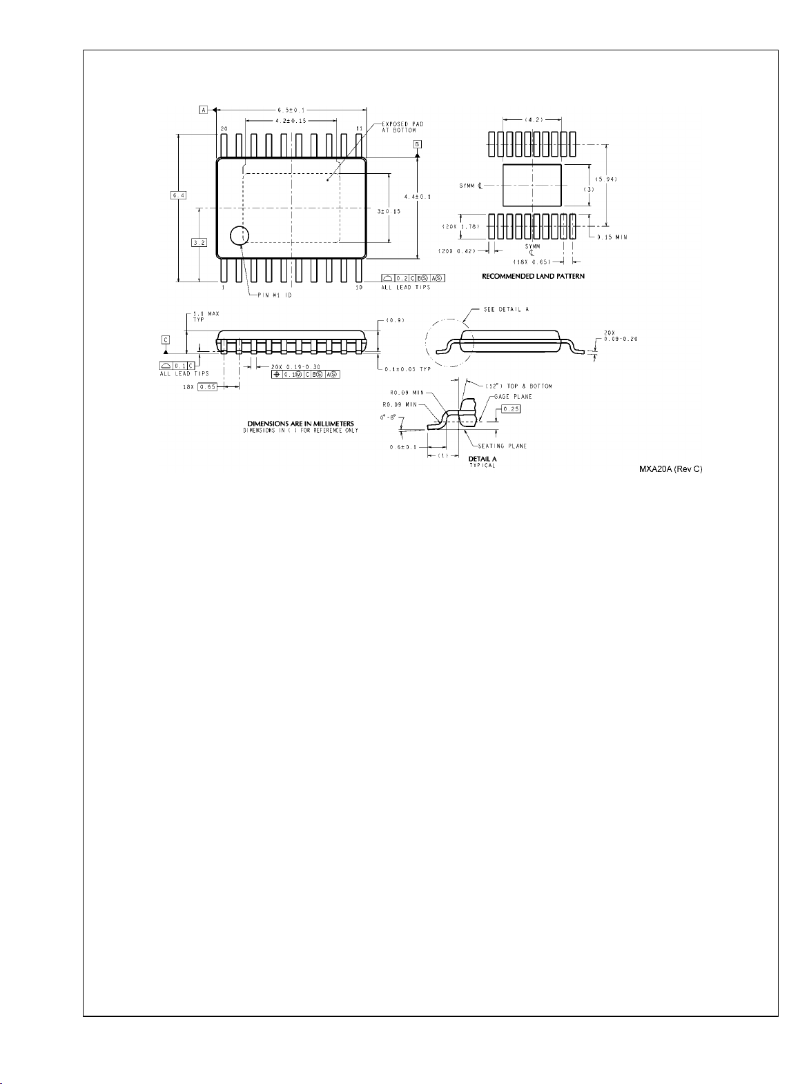
Physical Dimensions inches (millimeters) unless otherwise noted
LM5118
TSSOP-20EP Outline Drawing
NS Package Number MXA20A
www.national.com 24

Notes
LM5118
25 www.national.com

Notes
For more National Semiconductor product information and proven design tools, visit the following Web sites at:
Products Design Support
Amplifiers www.national.com/amplifiers WEBENCH www.national.com/webench
Audio www.national.com/audio Analog University www.national.com/AU
Clock Conditioners www.national.com/timing App Notes www.national.com/appnotes
Data Converters www.national.com/adc Distributors www.national.com/contacts
Displays www.national.com/displays Green Compliance www.national.com/quality/green
Ethernet www.national.com/ethernet Packaging www.national.com/packaging
Interface www.national.com/interface Quality and Reliability www.national.com/quality
LVDS www.national.com/lvds Reference Designs www.national.com/refdesigns
Power Management www.national.com/power Feedback www.national.com/feedback
Switching Regulators www.national.com/switchers
LDOs www.national.com/ldo
LED Lighting www.national.com/led
PowerWise www.national.com/powerwise
Serial Digital Interface (SDI) www.national.com/sdi
Temperature Sensors www.national.com/tempsensors
Wireless (PLL/VCO) www.national.com/wireless
THE CONTENTS OF THIS DOCUMENT ARE PROVIDED IN CONNECTION WITH NATIONAL SEMICONDUCTOR CORPORATION
(“NATIONAL”) PRODUCTS. NATIONAL MAKES NO REPRESENTATIONS OR WARRANTIES WITH RESPECT TO THE ACCURACY
OR COMPLETENESS OF THE CONTENTS OF THIS PUBLICATION AND RESERVES THE RIGHT TO MAKE CHANGES TO
SPECIFICATIONS AND PRODUCT DESCRIPTIONS AT ANY TIME WITHOUT NOTICE. NO LICENSE, WHETHER EXPRESS,
LM5118 Wide Voltage Range Buck-Boost Controller
IMPLIED, ARISING BY ESTOPPEL OR OTHERWISE, TO ANY INTELLECTUAL PROPERTY RIGHTS IS GRANTED BY THIS
DOCUMENT.
TESTING AND OTHER QUALITY CONTROLS ARE USED TO THE EXTENT NATIONAL DEEMS NECESSARY TO SUPPORT
NATIONAL’S PRODUCT WARRANTY. EXCEPT WHERE MANDATED BY GOVERNMENT REQUIREMENTS, TESTING OF ALL
PARAMETERS OF EACH PRODUCT IS NOT NECESSARILY PERFORMED. NATIONAL ASSUMES NO LIABILITY FOR
APPLICATIONS ASSISTANCE OR BUYER PRODUCT DESIGN. BUYERS ARE RESPONSIBLE FOR THEIR PRODUCTS AND
APPLICATIONS USING NATIONAL COMPONENTS. PRIOR TO USING OR DISTRIBUTING ANY PRODUCTS THAT INCLUDE
NATIONAL COMPONENTS, BUYERS SHOULD PROVIDE ADEQUATE DESIGN, TESTING AND OPERATING SAFEGUARDS.
EXCEPT AS PROVIDED IN NATIONAL’S TERMS AND CONDITIONS OF SALE FOR SUCH PRODUCTS, NATIONAL ASSUMES NO
LIABILITY WHATSOEVER, AND NATIONAL DISCLAIMS ANY EXPRESS OR IMPLIED WARRANTY RELATING TO THE SALE
AND/OR USE OF NATIONAL PRODUCTS INCLUDING LIABILITY OR WARRANTIES RELATING TO FITNESS FOR A PARTICULAR
PURPOSE, MERCHANTABILITY, OR INFRINGEMENT OF ANY PATENT, COPYRIGHT OR OTHER INTELLECTUAL PROPERTY
RIGHT.
LIFE SUPPORT POLICY
NATIONAL’S PRODUCTS ARE NOT AUTHORIZED FOR USE AS CRITICAL COMPONENTS IN LIFE SUPPORT DEVICES OR
SYSTEMS WITHOUT THE EXPRESS PRIOR WRITTEN APPROVAL OF THE CHIEF EXECUTIVE OFFICER AND GENERAL
COUNSEL OF NATIONAL SEMICONDUCTOR CORPORATION. As used herein:
Life support devices or systems are devices which (a) are intended for surgical implant into the body, or (b) support or sustain life and
whose failure to perform when properly used in accordance with instructions for use provided in the labeling can be reasonably expected
to result in a significant injury to the user. A critical component is any component in a life support device or system whose failure to perform
can be reasonably expected to cause the failure of the life support device or system or to affect its safety or effectiveness.
National Semiconductor and the National Semiconductor logo are registered trademarks of National Semiconductor Corporation. All other
brand or product names may be trademarks or registered trademarks of their respective holders.
Copyright© 2008 National Semiconductor Corporation
For the most current product information visit us at www.national.com
www.national.com
National Semiconductor
Americas Technical
Support Center
Email: support@nsc.com
Tel: 1-800-272-9959
National Semiconductor Europe
Technical Support Center
Email: europe.support@nsc.com
German Tel: +49 (0) 180 5010 771
English Tel: +44 (0) 870 850 4288
National Semiconductor Asia
Pacific Technical Support Center
Email: ap.support@nsc.com
National Semiconductor Japan
Technical Support Center
Email: jpn.feedback@nsc.com
 Loading...