

April 2007
LM5116
Wide Range Synchronous Buck Controller
General Description
The LM5116 is a synchronous buck controller intended for
step-down regulator applications from a high voltage or widely
varying input supply. The control method is based upon current mode control utilizing an emulated current ramp. Current
mode control provides inherent line feed-forward, cycle by
cycle current limiting and ease of loop compensation. The use
of an emulated control ramp reduces noise sensitivity of the
pulse-width modulation circuit, allowing reliable control of
very small duty cycles necessary in high input voltage applications. The operating frequency is programmable from
50kHz to 1MHz. The LM5116 drives external high-side and
low-side NMOS power switches with adaptive dead-time control. A user-selectable diode emulation mode enables discontinuous mode operation for improved efficiency at light load
conditions. A low quiescent current shutdown disables the
controller and consumes less than 10µA of total input current.
Additional features include a high voltage bias regulator, automatic switch-over to external bias for improved efficiency,
thermal shutdown, frequency synchronization, cycle by cycle
current limit and adjustable line under-voltage lockout. The
device is available in a power enhanced TSSOP-20 package
featuring an exposed die attach pad to aid thermal dissipation.
Features
■
Emulated peak current mode
■
Wide operating range up to 100V
■
Low IQ shutdown (<10µA)
■
Drives standard or logic level MOSFETs
■
Robust 3.5A peak gate drive
■
Free-run or synchronous operation to 1MHz
■
Optional diode emulation mode
■
Programmable output from 1.215V to 80V
■
Precision 1.5% voltage reference
■
Programmable current limit
■
Programmable soft-start
■
Programmable line under-voltage lockout
■
Automatic switch to external bias supply
■
TSSOP-20EP exposed pad
■
Thermal shutdown
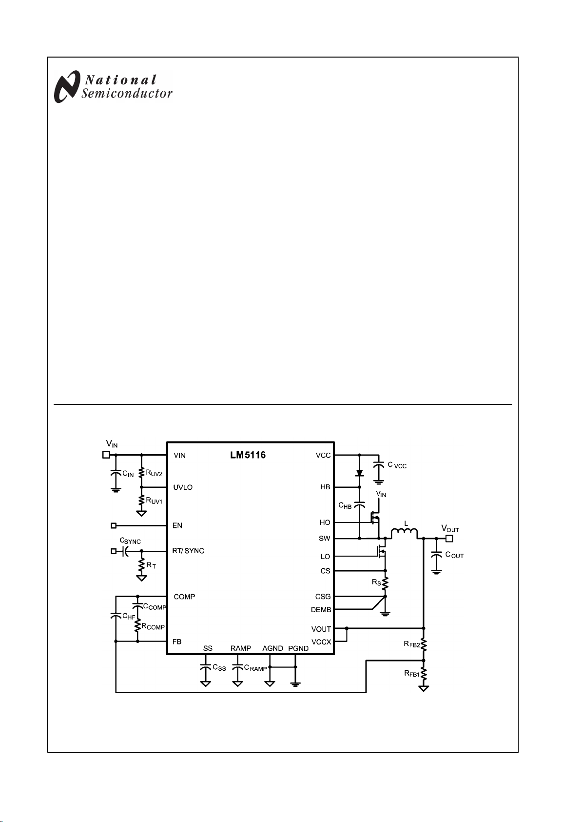
Typical Application
30007501
© 2007 National Semiconductor Corporation 300075 www.national.com
LM5116 Wide Range Synchronous Buck Controller
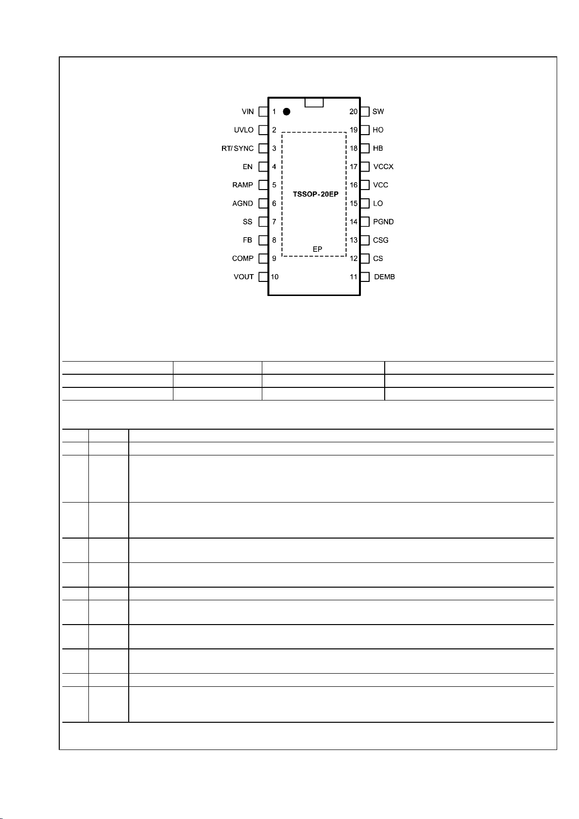
Connection Diagram
30007502
Top View
See NS Package Numbers MXA20A
Ordering Information
Ordering Number Package Type NSC Package Drawing Supplied As
LM5116MH TSSOP-20EP MXA20A 73 Units Per Anti-Static Tube
LM5116MHX TSSOP-20EP MXA20A 2500 units shipped as Tape & Reel
Pin Descriptions
Pin Name Description
1 VIN Chip supply voltage, input voltage monitor and input to the VCC regulator.
2 UVLO If the UVLO pin is below 1.215V, the regulator will be in standby mode (VCC regulator running, switching regulator
disabled). If the UVLO pin voltage is above 1.215V, the regulator is operational. An external voltage divider can be
used to set an under-voltage shutdown threshold. There is a fixed 5µA pull up current on this pin when EN is high.
UVLO is pulled to ground in the event a current limit condition exists for 256 clock cycles.
3 RT/
SYNC
The internal oscillator is set with a single resistor between this pin and the AGND pin. The recommended frequency
range is 50kHz to 1MHz. The internal oscillator can be synchronized to an external clock by AC coupling a positive
edge onto this node.
4 EN If the EN pin is below 0.5V, the regulator will be in a low power state drawing less than 10µA from VIN. EN must be
pulled above 3.3V for normal operation.
5 RAMP Ramp control signal. An external capacitor connected between this pin and the AGND pin sets the ramp slope used
for current mode control.
6 AGND Analog ground.
7 SS An external capacitor and an internal 10µA current source set the soft start time constant for the rise of the error amp
reference. The SS pin is held low during VCC < 4.5V, UVLO < 1.215V, EN input low or thermal shutdown.
8 FB Feedback signal from the regulated output. This pin is connected to the inverting input of the internal error amplifier.
The regulation threshold is 1.215V.
9 COMP Output of the internal error amplifier. The loop compensation network should be connected between this pin and the
FB pin.
10 VOUT Output monitor. Connect directly to the output voltage.
11 DEMB Low-side MOSFET source voltage monitor for diode emulation. For start-up into a pre-biased load, tie this pin to
ground at the CSG connection. For fully synchronous operation, use an external series resistor between DEMB and
ground to raise the diode emulation threshold above the low-side SW on-voltage.
www.national.com 2
LM5116
Pin Name Description
12 CS Current sense amplifier input. Connect to the top of the current sense resistor or the drain of the low-sided MOSFET
if R
DS(ON)
current sensing is used.
13 CSG Current sense amplifier input. Connect to the bottom of the sense resistor or the source of the low-side MOSFET if
R
DS(ON)
current sensing is used.
14 PGND Power ground.
15 LO Connect to the gate of the low-side synchronous MOSFET through a short, low inductance path.
16 VCC Locally decouple to PGND using a low ESR/ESL capacitor located as close to the controller as possible.
17 VCCX Optional input for an externally supplied VCC. If VCCX > 4.5V, VCCX is internally connected to VCC and the internal
VCC regulator is disabled. If VCCX is unused, it should be connected to ground.
18 HB High-side driver supply for bootstrap gate drive. Connect to the cathode of the bootstrap diode and the positive
terminal of the bootstrap capacitor. The bootstrap capacitor supplies current to charge the high-side MOSFET gate
and should be placed as close to the controller as possible.
19 HO Connect to the gate of the high-side synchronous MOSFET through a short, low inductance path
20 SW Switch node. Connect to the negative terminal of the bootstrap capacitor and the source terminal of the high-side
MOSFET.
EP EP Exposed pad. Solder to ground plane.
3 www.national.com
LM5116
Absolute Maximum Ratings (Note 1)
If Military/Aerospace specified devices are required,
please contact the National Semiconductor Sales Office/
Distributors for availability and specifications.
VIN to GND -0.3V to 100V
VCC, VCCX, UVLO to GND (Note 3) -0.3 to 16V
SW, CS to GND -3.0 to 100V
HB to SW -0.3 to 16V
HO to SW -0.3 to HB+0.3V
VOUT to GND -0.3 to 100V
CSG to GND -1V to 1V
LO to GND -0.3 to VCC+0.3V
SS to GND -0.3 to 7V
FB to GND -0.3 to 7V
DEMB to GND -0.3 to VCC
RT to GND -0.3 to 7V
EN to GND -0.3 to 100V
ESD Rating
HBM (Note 2) 2 kV
Storage Temperature Range -55°C to +150°C
Junction Temperature +150°C
Operating Ratings (Note 1)
VIN 6V to 100V
VCC, VCCX 4.75V to 15V
HB to SW 4.75V to 15V
DEMB to GND -0.3V to 2V
Junction Temperature -40°C to +125°C
Note: RAMP, COMP are output pins. As such they are not specified to have
an external voltage applied.
Electrical Characteristics Limits in standard type are for T
J
= 25°C only; limits in boldface type apply over the
junction temperature range of -40°C to +125°C and are provided for reference only. Unless otherwise specified, the following
conditions apply: VIN = 48V, VCC = 7.4V, VCCX = 0V, EN = 5V, RT = 16kΩ, no load on LO and HO.
Symbol Parameter Conditions Min Typ Max Units
VIN Supply
I
BIAS
VIN Operating Current VCCX = 0V, VIN = 48V 5 7 mA
VCCX = 0V, VIN = 100V 5.9 8 mA
I
BIASX
VIN Operating Current VCCX = 5V, VIN = 48V 1.2 1.7 mA
VCCX = 5V, VIN = 100V 1.6 2.3 mA
I
STDBY
VIN Shutdown Current EN = 0V, VIN = 48V 1 10 µA
EN = 0V, VIN = 100V 1 µA
VCC Regulator
V
CC(REG)
VCC Regulation 7.1 7.4 7.7 V
VCC LDO Mode Turn-off 10.6 V
VCC Regulation VIN = 6V 5.0 5.9 6.0 V
VCC Sourcing Current Limit VCC = 0V 15 26 mA
VCCX Switch Threshold VCCX Rising 4.3 4.5 4.7 V
VCCX Switch Hysteresis 0.25 V
VCCX Switch R
DS(ON)
ICCX = 10mA 3.8 6.2
Ω
VCCX Leakage VCCX = 0V -200 nA
VCCX Pull- down Resistance VCCX = 3V 100
kΩ
VCC Under-voltage Threshold VCC Rising 4.3 4.5 4.7 V
VCC Under-voltage Hysteresis 0.2 V
HB DC Bias Current HB-SW = 15V 125 200 µA
EN Input
VIL max EN Input Low Threshold 0.5 V
VIH min EN Input High Threshold 3.3 V
EN Input Bias Current VEN = 3V -7.5 -3 1 µA
EN Input Bias Current VEN = 0.5V -1 0 1 µA
EN Input Bias Current VEN = 100V 20 90 µA
UVLO Thresholds
UVLO Standby Threshold UVLO Rising 1.170 1.215 1.262 V
UVLO Threshold Hysteresis 0.1 V
UVLO Pull-up Current Source UVLO = 0V 5.4 µA
UVLO Pull-down R
DS(ON)
80 210
Ω
www.national.com 4
LM5116
Symbol Parameter Conditions Min Typ Max Units
Soft Start
SS Current Source SS = 0V 8 11 14 µA
SS Diode Emulation Ramp Disable
Threshold
SS Rising 3 V
SS to FB Offset FB = 1.25V 160 mV
SS Output Low Voltage Sinking 100µA, UVLO = 0V 45 mV
Error Amplifier
V
REF
FB Reference Voltage Measured at FB pin, FB =
COMP
1.195 1.215 1.231 V
FB Input Bias Current FB = 2V 15 500 nA
COMP Sink/Source Current 3 mA
A
OL
DC Gain 80 dB
f
BW
Unity Gain Bandwidth 3 MHz
PWM Comparators
t
HO(OFF)
Forced HO Off-time 320 450 580 ns
t
ON(min)
Minimum HO On-time VIN = 80V, C
RAMP
= 50pF 100 ns
Oscillator
f
SW1
Frequency 1
RT = 16kΩ
180 200 220 kHz
f
SW2
Frequency 2
RT = 5kΩ
480 535 590 kHz
RT output voltage 1.191 1.215 1.239 V
RT sync positive threshold 3.0 3.5 4.0 V
Current Limit
V
CS(TH)
Cycle-by-cycle Sense Voltage
Threshold (CSG-CS)
VCCX = 0V, RAMP = 0V 94 110 126 mV
V
CS(THX)
Cycle-by-cycle Sense Voltage
Threshold (CSG-CS)
VCCX = 5V, RAMP = 0V 105 122 139 mV
CS Bias Current CS = 100V -1 1 µA
CS Bias Current CS = 0V 90 125 µA
CSG Bias Current CSG = 0V 90 125 µA
Current Limit Fault Timer
RT = 16kΩ, (200kHz), (256
clock cycles)
1.28 ms
RAMP Generator
I
R1
RAMP Current 1 VIN = 60V, VOUT=10V 235 285 335 µA
I
R2
RAMP Current 2 VIN = 10V, VOUT = 10V 21 28 35 µA
VOUT Bias Current VOUT = 36V 200 µA
RAMP Output Low Voltage VIN = 60V, VOUT = 10V 265 mV
Diode Emulation
SW Zero Cross Threshold -6 mV
DEMB Output Current DEMB = 0V, SS = 1.25V 1.6 2.7 3.8 µA
DEMB Output Current DEMB =0V, SS = 2.8V 28 38 48 µA
DEMB Output Current DEMB = 0V, SS = Regulated
by FB
45 65 85 µA
LO Gate Driver
V
OLL
LO Low-state Output Voltage ILO = 100mA 0.08 0.17 V
V
OHL
LO High-state Output Voltage ILO = -100mA, V
OHL
= VCC -
V
LO
0.25 V
LO Rise Time C-load = 1000pF 18 ns
LO Fall Time C-load = 1000pF 12 ns
I
OHL
Peak LO Source Current VLO = 0V 1.8 A
I
OLL
Peak LO Sink Current VLO = VCC 3.5 A
5 www.national.com
LM5116
Symbol Parameter Conditions Min Typ Max Units
HO Gate Driver
V
OLH
HO Low-state Output Voltage IHO = 100mA 0.17 0.27 V
V
OHH
HO High-state Output Voltage IHO = -100mA, V
OHH
= VHB –
V
HO
0.45 V
HO Rise Time C-load = 1000pF 19 ns
HO High-side Fall Time C-load = 1000pF 13 ns
I
OHH
Peak HO Source Current VHO = 0V 1 A
I
OLH
Peak HO Sink Current VHO = VCC 2.2 A
HB to SW under-voltage 3 V
Switching Characteristics
LO Fall to HO Rise Delay C-load = 0 75 ns
HO Fall to LO Rise Delay C-load = 0 70 ns
Thermal
T
SD
Thermal Shutdown Rising 170 °C
Thermal Shutdown Hysteresis 15 °C
θ
JA
Junction to Ambient 40 °C/W
θ
JC
Junction to Case 4 °C/W
Note 1: Absolute Maximum Ratings indicate limits beyond which damage to the component may occur. Operating Ratings are conditions under which operation
of the device is guaranteed. Operating Ratings do not imply guaranteed performance limits. For guaranteed performance limits and associated test conditions,
see the Electrical Characteristics tables.
Note 2: The human body model is a 100pF capacitor discharged through a 1.5kΩ resistor into each pin. LO, HO and HB are rated at 1kV. 2kV rating for all pins
except VIN which is rated for 1.5kV.
Note 3: These pins must not exceed VIN.
www.national.com 6
LM5116
Typical Performance Characteristics
Typical Application Circuit Efficiency
30007503
Driver Source Current vs VCC
30007504
Driver Dead-time vs Temperature
30007505
HO High R
DS(ON)
vs VCC
30007506
Driver Sink Current vs VCC
30007507
HO Low R
DS(ON)
vs VCC
30007508
7 www.national.com
LM5116
LO High R
DS(ON)
vs VCC
30007509
EN Input Threshold vs Temperature
30007510
LO Low R
DS(ON)
vs VCC
30007511
HB to SW UVLO vs Temperature
30007512
Forced HO Off-time vs Temperature
VCCX = 5V
30007513
HB DC Bias Current vs Temperature
30007514
www.national.com 8
LM5116

Frequency vs R
T
30007515
Error Amp Gain vs Frequency
30007516
Frequency vs Temperature
30007517
Error Amp Phase vs Frequency
30007518
Frequency vs Temperature
30007519
Current Limit Threshold vs. Temperature
30007520
9 www.national.com
LM5116

VIN Operating Current vs Temperature
30007521
VCC vs Temperature
30007522
VCC UVLO vs Temperature
30007523
VCC vs VIN
30007524
VCC vs ICC
30007525
VCCX Switch R
DS(ON)
vs VCCX
30007526
www.national.com 10
LM5116

Block Diagram and Typical Application Circuit
30007527
FIGURE 1.
11 www.national.com
LM5116

Detailed Operating Description
The LM5116 high voltage switching regulator features all of
the functions necessary to implement an efficient high voltage
buck regulator using a minimum of external components. This
easy to use regulator integrates high-side and low-side MOSFET drivers capable of supplying peak currents of 2 Amps.
The regulator control method is based on current mode control utilizing an emulated current ramp. Emulated peak current
mode control provides inherent line feed-forward, cycle by
cycle current limiting and ease of loop compensation. The use
of an emulated control ramp reduces noise sensitivity of the
pulse-width modulation circuit, allowing reliable processing of
the very small duty cycles necessary in high input voltage applications. The operating frequency is user programmable
from 50kHz to 1MHz. An oscillator/synchronization pin allows
the operating frequency to be set by a single resistor or synchronized to an external clock. Fault protection features include current limiting, thermal shutdown and remote shutdown capability. An under-voltage lockout input allows
regulator shutdown when the input voltage is below a user
selected threshold, and an enable function will put the regulator into an extremely low current shutdown via the enable
input. The TSSOP-20EP package features an exposed pad
to aid in thermal dissipation.
High Voltage Start-Up Regulator
The LM5116 contains a dual mode internal high voltage startup regulator that provides the VCC bias supply for the PWM
controller and a boot-strap gate drive for the high-side buck
MOSFET. The input pin (VIN) can be connected directly to an
input voltage source as high as 100 volts. For input voltages
below 10.6V, a low dropout switch connects VCC directly to
VIN. In this supply range, VCC is approximately equal to VIN.
For VIN voltages greater than 10.6V, the low dropout switch
is disabled and the VCC regulator is enabled to maintain VCC
at approximately 7.4V. The wide operating range of 6V to
100V is achieved through the use of this dual mode regulator.
The output of the VCC regulator is current limited to 26mA
(typical). Upon power-up, the regulator sources current into
the capacitor connected to the VCC pin. When the voltage at
the VCC pin exceeds 4.5V and the UVLO pin is greater than
1.215V, the output switch is enabled and a soft-start sequence begins. The output switch remains enabled until VCC
falls below 4.5V, EN is pulled low, the UVLO pin falls below
1.215V or the die temperature exceeds the thermal limit
threshold.
30007548
FIGURE 2. VCCX Bias Supply with Additional Inductor
Winding
An output voltage derived bias supply can be applied to the
VCCX pin to reduce the IC power dissipation. If the bias sup-
ply voltage is greater than 4.5V, the internal regulator will
essentially shut off, reducing the IC power dissipation. The
VCC regulator series pass transistor includes a diode between VCC and VIN that should not be forward biased in
normal operation. For an output voltage between 5V and 15V,
VOUT can be connected directly to VCCX. For VOUT < 5V,
a bias winding on the output inductor can be added to VOUT.
If the bias winding can supply VCCX greater than VIN, an
external blocking diode is required from the input power supply to the VIN pin to prevent VCC from discharging into the
input supply.
In high voltage applications extra care should be taken to ensure the VIN pin does not exceed the absolute maximum
voltage rating of 100V. During line or load transients, voltage
ringing on the VIN line that exceeds the Absolute Maximum
Ratings can damage the IC. Both careful PC board layout and
the use of quality bypass capacitors located close to the VIN
and GND pins are essential.
Enable
The LM5116 contains an enable function allowing a very low
input current shutdown. If the enable pin is pulled below 0.5V,
the regulator enters shutdown, drawing less than 10µA from
the VIN pin. Raising the EN input above 3.3V returns the regulator to normal operation. The EN pin can be tied directly to
VIN if this function is not needed. It must not be left floating.
A 1MΩ pull-up resistor to VIN can be used to interface with
an open collector control signal.
30007549
FIGURE 3. Enable Circuit
30007550
FIGURE 4. EN Bias Current vs Voltage
www.national.com 12
LM5116

UVLO
An under-voltage lockout pin is provided to disable the regulator without entering shutdown. If the UVLO pin is pulled
below 1.215V, the regulator enters a standby mode of operation with the soft-start capacitor discharged and outputs
disabled, but with the VCC regulator running. If the UVLO input is pulled above 1.215V, the controller will resume normal
operation. A voltage divider from input to ground can be used
to set a VIN threshold to disable the supply in brown-out conditions or for low input faults. The UVLO pin has a 5µA internal
pull up current that allows this pin to left open if the input under-voltage lockout function is not needed.
The UVLO pin can also be used to implement a “hiccup” current limit. If a current limit fault exists for more than 256
consecutive clock cycles, the UVLO pin will be internally
pulled down to 200mV and then released. A capacitor to
ground connected to the UVLO pin will set the timing for hiccup mode current limit. When this feature is used in conjunction with the voltage divider, a diode across the top resistor
may be used to discharge the capacitor in the event of an
input under-voltage condition.
Oscillator and Sync Capability
The LM5116 oscillator frequency is set by a single external
resistor connected between the RT/SYNC pin and the AGND
pin. The resistor should be located very close to the device
and connected directly to the pins of the IC (RT/SYNC and
AGND). To set a desired oscillator frequency (fSW), the necessary value for the resistor can be calculated from the following equation:
Where T = 1 / fSW and RT is in ohms. 450ns represents the
fixed minimum off time.
The RT/SYNC pin can be used to synchronize the internal
oscillator to an external clock. The external clock must be a
higher frequency than the free-running frequency set by the
RT resistor. The internal oscillator can be synchronized to an
external clock by AC coupling a positive edge into the RT/
SYNC pin. The voltage at the RT/SYNC pin is nominally
1.215V and must exceed 4V to trip the internal synchronization pulse detection. A 5V amplitude signal and 100pF coupling capacitor are recommended. The free-running frequency should be set nominally 15% below the external clock.
Synchronizing above twice the free-running frequency may
result in abnormal behavior of the pulse width modulator.
Error Amplifier and PWM
Comparator
The internal high-gain error amplifier generates an error signal proportional to the difference between the regulated output voltage and an internal precision reference (1.215V). The
output of the error amplifier is connected to the COMP pin
allowing the user to provide loop compensation components,
generally a type II network. This network creates a pole at
very low frequency, a mid-band zero, and a noise reducing
high frequency pole. The PWM comparator compares the
emulated current sense signal from the RAMP generator to
the error amplifier output voltage at the COMP pin.
Ramp Generator
The ramp signal used in the pulse width modulator for current
mode control is typically derived directly from the buck switch
current. This switch current corresponds to the positive slope
portion of the inductor current. Using this signal for the PWM
ramp simplifies the control loop transfer function to a single
pole response and provides inherent input voltage feed-forward compensation. The disadvantage of using the buck
switch current signal for PWM control is the large leading
edge spike due to circuit parasitics that must be filtered or
blanked. Also, the current measurement may introduce significant propagation delays. The filtering, blanking time and
propagation delay limit the minimal achievable pulse width. In
applications where the input voltage may be relatively large
in comparison to the output voltage, controlling small pulse
widths and duty cycles is necessary for regulation. The
LM5116 utilizes a unique ramp generator which does not actually measure the buck switch current but rather reconstructs
the signal. Representing or emulating the inductor current
provides a ramp signal to the PWM comparator that is free of
leading edge spikes and measurement or filtering delays. The
current reconstruction is comprised of two elements, a sample-and-hold DC level and an emulated current ramp.
30007546
FIGURE 5. Composition of Current Sense Signal
13 www.national.com
LM5116

The sample-and-hold DC level is derived from a measurement of the recirculating current through either the low-side
MOSFET or current sense resistor. The voltage level across
the MOSFET or sense resistor is sampled and held just prior
to the onset of the next conduction interval of the buck switch.
The current sensing and sample-and-hold provide the DC
level of the reconstructed current signal. The positive slope
inductor current ramp is emulated by an external capacitor
connected from the RAMP pin to the AGND and an internal
voltage controlled current source. The ramp current source
that emulates the inductor current is a function of the VIN and
VOUT voltages per the following equation:
IR = 5µA/V x (VIN-VOUT) + 25µA
Proper selection of the RAMP capacitor (C
RAMP
) depends upon the value of the output inductor (L) and the current sense
resistor (RS). For proper current emulation, the DC sample
and hold value and the ramp amplitude must have the same
dependence on the load current. That is:
Where gm is the ramp generator transconductance (5µA/V)
and A is the current sense amplifier gain (10V/V). The ramp
capacitor should be located very close to the device and connected directly to the pins of the IC (RAMP and AGND).
The difference between the average inductor current and the
DC value of the sampled inductor current can cause instability
for certain operating conditions. This instability is known as
sub-harmonic oscillation, which occurs when the inductor ripple current does not return to its initial value by the start of
next switching cycle. Sub-harmonic oscillation is normally
characterized by observing alternating wide and narrow pulses at the switch node. Adding a fixed slope voltage ramp
(slope compensation) to the current sense signal prevents
this oscillation. The 25µA of offset current provided from the
emulated current source adds the optimal slope compensation to the ramp signal for a 5V output. For higher output
voltages, additional slope compensation may be required. In
these applications, the ramp capacitor can be decreased from
its nominal value to increase the ramp slope compensation.
30007547
FIGURE 6. R
DS(ON)
Current Sensing without Diode
Emulation
The DC current sample is obtained using the CS and CSG
pins connected to either a source sense resistor (RS) or the
R
DS(ON)
of the low-side MOSFET. For R
DS(ON)
sensing, RS =
R
DS(ON)
of the low-side MOSFET. In this case it is sometimes
helpful to adjust the current sense amplifier gain (A) to a lower
value in order to obtain the desired current limit. Adding external resistors RG in series with CS and CSG, the current
sense amplifier gain A becomes:
Current Limit
The LM5116 contains a current limit monitoring scheme to
protect the circuit from possible over-current conditions.
When set correctly, the emulated current sense signal is proportional to the buck switch current with a scale factor determined by the current limit sense resistor. The emulated ramp
signal is applied to the current limit comparator. If the emulated ramp signal exceeds 1.6V, the current cycle is terminated (cycle-by-cycle current limiting). Since the ramp
amplitude is proportional to VIN - V
OUT
, if V
OUT
is shorted, there
is an immediate reduction in duty cycle. To further protect the
external switches during prolonged current limit conditions,
an internal counter counts clock pulses when in current limit.
When the counter detects 256 consecutive clock cycles, the
regulator enters a low power dissipation hiccup mode of current limit. The regulator is shut down by momentarily pulling
UVLO low, and the soft-start capacitor discharged. The regulator is restarted with a full soft-start cycle once UVLO
charges back to 1.215V. This process is repeated until the
fault is removed. The hiccup off-time can be controlled by a
capacitor to ground on the UVLO pin. In applications with low
output inductance and high input voltage, the switch current
may overshoot due to the propagation delay of the current
limit comparator. If an overshoot should occur, the sampleand-hold circuit will detect the excess recirculating current. If
the sample-and-hold DC level exceeds the internal current
limit threshold, the buck switch will be disabled and skip pulses until the current has decayed below the current limit threshold. This approach prevents current runaway conditions due
to propagation delays or inductor saturation since the inductor
current is forced to decay following any current overshoot.
www.national.com 14
LM5116

30007543
FIGURE 7. Current Limit and Ramp Circuit
Using a current sense resistor in the source of the low-side
MOSFET provides superior current limit accuracy compared
to R
DS(ON)
sensing. R
DS(ON)
sensing is far less accurate due
to the large variation of MOSFET R
DS(ON)
with temperature
and part-to-part variation. The CS and CSG pins should be
Kelvin connected to the current sense resistor or MOSFET
drain and source.
The peak current which triggers the current limit comparator
is:
Where tON is the on-time of the high-side MOSFET. The 1.1V
threshold is the difference between the 1.6V reference at the
current limit comparator and the 0.5V offset at the current
sense amplifier. This offset at the current sense amplifier allows the inductor ripple current to go negative by 0.5V / (A x
RS) when running full synchronous operation.
Current limit hysteresis prevents chatter around the threshold
when VCCX is powered from VOUT. When 4.5V < VCC <
5.8V, the 1.6V reference is increased to 1.72V. The peak current which triggers the current limit comparator becomes:
This has the effect of a 10% fold-back of the peak current
during a short circuit when VCCX is powered from a 5V output.
Soft-Start and Diode Emulation
The soft-start feature allows the regulator to gradually reach
the initial steady state operating point, thus reducing start-up
stresses and surges. The LM5116 will regulate the FB pin to
the SS pin voltage or the internal 1.215V reference, whichever
is lower. At the beginning of the soft-start sequence when SS
= 0V, the internal 10µA soft-start current source gradually increases the voltage of an external soft-start capacitor (CSS)
connected to the SS pin resulting in a gradual rise of FB and
the output voltage.
30007544
FIGURE 8. Diode Emulation Control
During this initial charging of CSS to the internal reference
voltage, the LM5116 will force diode emulation. That is, the
low-side MOSFET will turn off for the remainder of a cycle if
the sensed inductor current becomes negative. The inductor
current is sensed by monitoring the voltage between SW and
DEMB. As the SS capacitor continues to charge beyond
1.215V to 3V, the DEMB bias current will increase from 0µA
up to 40µA. With the use of an external DEMB resistor
(R
DEMB
), the current sense threshold for diode emulation will
increase resulting in the gradual transition to synchronous
operation. Forcing diode emulation during soft-start allows
the LM5116 to start up into a pre-biased output without unnecessarily discharging the output capacitor. Full synchronous operation is obtained if the DEMB pin is always
biased to a higher potential than the SW pin when LO is high.
R
DEMB
= 10kΩ will bias the DEMB pin to 0.45V minimum,
which is adequate for most applications. The DEMB bias potential should always be kept below 2V. When R
DEMB
= 0Ω,
the LM5116 will always run in diode emulation.
Once SS charges to 3V the SS latch is set, increasing the
DEMB bias current to 65µA. An amplifier is enabled that regulates SS to 160mV above the FB voltage. This feature can
prevent overshoot of the output voltage in the event the output
15 www.national.com
LM5116

voltage momentarily dips out of regulation. When a fault is
detected (VCC under-voltage, UVLO pin < 1.215, or EN = 0V)
the soft-start capacitor is discharged. Once the fault condition
is no longer present, a new soft-start sequence begins.
HO Ouput
The LM5116 contains a high current, high-side driver and associated high voltage level shift. This gate driver circuit works
in conjunction with an external diode and bootstrap capacitor.
A 1µF ceramic capacitor, connected with short traces between the HB pin and SW pin, is recommended. During the
off-time of the high-side MOSFET, the SW pin voltage is approximately -0.5V and the bootstrap capacitor charges from
VCC through the external bootstrap diode. When operating
with a high PWM duty cycle, the buck switch will be forced off
each cycle for 450ns to ensure that the bootstrap capacitor is
recharged.
The LO and HO outputs are controlled with an adaptive deadtime methodology which insures that both outputs are never
enabled at the same time. When the controller commands HO
to be enabled, the adaptive block first disables LO and waits
for the LO voltage to drop below approximately 25% of VCC.
HO is then enabled after a small delay. Similarly, LO is enabled once HO has discharged. This methodology insures
adequate dead-time for any size MOSFET.
Thermal Protection
Internal thermal shutdown circuitry is provided to protect the
integrated circuit in the event the maximum junction temperature is exceeded. When activated, typically at 170°C, the
controller is forced into a low power reset state, disabling the
output driver and the bias regulator. This is designed to prevent catastrophic failures from accidental device overheating.
Application Information
EXTERNAL COMPONENTS
The procedure for calculating the external components is illustrated with the following design example. The Bill of Materials for this design is listed in Table 1. The circuit shown in
Figure 15 is configured for the following specifications:
•
Output voltage = 5V
•
Input voltage = 7V to 60V
•
Maximum load current = 7A
•
Switching frequency = 250kHz
Simplified equations are used as a general guideline for the
design method. Comprehensive equations are provided at
the end of this section.
TIMING RESISTOR
RT sets the oscillator switching frequency. Generally, higher
frequency applications are smaller but have higher losses.
Operation at 250kHz was selected for this example as a reasonable compromise for both small size and high efficiency.
The value of RT for 250kHz switching frequency can be calculated as follows:
The nearest standard value of 12.4kΩ was chosen for RT.
OUTPUT INDUCTOR
The inductor value is determined based on the operating frequency, load current, ripple current and the input and output
voltages.
30007545
FIGURE 9. Inductor Current
Knowing the switching frequency (fSW), maximum ripple current (IPP), maximum input voltage (V
IN(MAX)
) and the nominal
output voltage (V
OUT
), the inductor value can be calculated:
The maximum ripple current occurs at the maximum input
voltage. Typically, IPP is 20% to 40% of the full load current.
When running diode emulation mode, the maximum ripple
current should be less than twice the minimum load current.
For full synchronous operation, higher ripple current is acceptable. Higher ripple current allows for a smaller inductor
size, but places more of a burden on the output capacitor to
smooth the ripple current for low output ripple voltage. For this
example, 40% ripple current was chosen for a smaller sized
inductor.
The nearest standard value of 6µH will be used. The inductor
must be rated for the peak current to prevent saturation. During normal operation, the peak current occurs at maximum
load current plus maximum ripple. During overload conditions
with properly scaled component values, the peak current is
limited to V
CS(TH)
/ RS (See next section). At the maximum
input voltage with a shorted output, the valley current must fall
below V
CS(TH)
/ RS before the high-side MOSFET is allowed
to turn on. The peak current in steady state will increase to
V
IN(MAX)
x t
ON(min)
/ L above this level. The chosen inductor
must be evaluated for this condition, especially at elevated
temperature where the saturation current rating may drop significantly.
CURRENT SENSE RESISTOR
The current limit is set by the current sense resistor value
(RS).
www.national.com 16
LM5116

For a 5V output, the maximum current sense signal occurs at
the minimum input voltage, so RS is calculated from:
For this example VCCX = 0V, so V
CS(TH)
= 0.11V. The current
sense resistor is calculated as:
The next lowest standard value of 10mΩ was chosen for RS.
RAMP CAPACITOR
With the inductor and sense resistor value selected, the value
of the ramp capacitor (C
RAMP
) necessary for the emulation
ramp circuit is:
Where L is the value of the output inductor in Henrys, gm is
the ramp generator transconductance (5µA/V), and A is the
current sense amplifier gain (10V/V). For the 5V output design
example, the ramp capacitor is calculated as:
The next lowest standard value of 270pF was selected for
C
RAMP
. A COG type capacitor with 5% or better tolerance is
recommended.
OUTPUT CAPACITORS
The output capacitors smooth the inductor ripple current and
provide a source of charge for transient loading conditions.
For this design example, five 100µF ceramic capacitors
where selected. Ceramic capacitors provide very low equivalent series resistance (ESR), but can exhibit a significant
reduction in capacitance with DC bias. From the
manufacturer’s data, the ESR at 250kHz is 2mΩ / 5 =
0.4mΩ, with a 36% reduction in capacitance at 5V. This is
verified by measuring the output ripple voltage and frequency
response of the circuit. The fundamental component of the
output ripple voltage is calculated as:
With typical values for the 5V design example:
INPUT CAPACITORS
The regulator supply voltage has a large source impedance
at the switching frequency. Good quality input capacitors are
necessary to limit the ripple voltage at the VIN pin while supplying most of the switch current during the on-time. When the
buck switch turns on, the current into the switch steps to the
valley of the inductor current waveform, ramps up to the peak
value, and then drops to zero at turn-off. The input capacitors
should be selected for RMS current rating and minimum ripple
voltage. A good approximation for the required ripple current
rating is I
RMS
> I
OUT
/ 2.
Quality ceramic capacitors with a low ESR were selected for
the input filter. To allow for capacitor tolerances and voltage
rating, four 2.2µF, 100V ceramic capacitors were used for the
typical application circuit. With ceramic capacitors, the input
ripple voltage will be triangular and peak at 50% duty cycle.
Taking into account the capacitance change with DC bias, the
input ripple voltage is approximated as:
When the converter is connected to an input power source, a
resonant circuit is formed by the line impedance and the input
capacitors. If step input voltage transients are expected near
the maximum rating of the LM5116, a careful evaluation of the
ringing and possible overshoot at the device VIN pin should
be completed. To minimize overshoot make CIN > 10 x LIN.
The characteristic source impedance and resonant frequency
are:
The converter exhibits a negative input impedance which is
lowest at the minimum input voltage:
The damping factor for the input filter is given by:
When δ = 1, the input filter is critically damped. This may be
difficult to achieve with practical component values. With δ <
0.2, the input filter will exhibit significant ringing. If δ is zero or
negative, there is not enough resistance in the circuit and the
input filter will sustain an oscillation. When operating near the
minimum input voltage, an aluminum electrolytic capacitor
across CIN may be needed to damp the input for a typical
bench test setup. Any parallel capacitor should be evaluated
for its RMS current rating. The current will split between the
ceramic and aluminum capacitors based on the relative
impedance at the switching frequency.
VCC CAPACITOR
The primary purpose of the VCC capacitor (C
VCC
) is to supply
the peak transient currents of the LO driver and bootstrap
diode (D1) as well as provide stability for the VCC regulator.
17 www.national.com
LM5116

These current peaks can be several amperes. The recommended value of C
VCC
should be no smaller than 0.47µF, and
should be a good quality, low ESR, ceramic capacitor located
at the pins of the IC to minimize potentially damaging voltage
transients caused by trace inductance. A value of 1µF was
selected for this design.
BOOTSTRAP CAPACITOR
The bootstrap capacitor (CHB) between the HB and SW pins
supplies the gate current to charge the high-side MOSFET
gate at each cycle’s turn-on as well as supplying the recovery
charge for the bootstrap diode (D1). These current peaks can
be several amperes. The recommended value of the bootstrap capacitor is at least 0.1µF, and should be a good quality,
low ESR, ceramic capacitor located at the pins of the IC to
minimize potentially damaging voltage transients caused by
trace inductance. The absolute minimum value for the bootstrap capacitor is calculated as:
Where Qg is the high-side MOSFET gate charge and ΔVHB is
the tolerable voltage droop on CHB, which is typically less than
5% of VCC. A value of 1µF was selected for this design.
SOFT START CAPACITOR
The capacitor at the SS pin (CSS) determines the soft-start
time, which is the time for the reference voltage and the output
voltage to reach the final regulated value. The value of C
SS
for a given time is determined from:
For this application, a value of 0.01µF was chosen for a softstart time of 1.2ms.
OUTPUT VOLTAGE DIVIDER
R
FB1
and R
FB2
set the output voltage level, the ratio of these
resistors is calculated from:
R
FB1
is typically 1.21kΩ for a divider current of 1mA. The di-
vider current can be reduced to 100µA with R
FB1
=12.1kΩ. For
the 5V output design example used here, R
FB1
= 1.21kΩ and
R
FB2
= 3.74kΩ.
UVLO DIVIDER
A voltage divider and filter can be connected to the UVLO pin
to set a minimum operating voltage V
IN(MIN)
for the regulator.
If this feature is required, the following procedure can be used
to determine appropriate resistor values for R
UV2
, R
UV1
and
CFT.
1.
R
UV2
must be large enough such that in the event of a
current limit, the internal UVLO switch can pull UVLO <
200mV. This can be guaranteed if:
R
UV2
> 500 x V
IN(MAX)
Where V
IN(MAX)
is the maximum input voltage and R
UV2
is in ohms.
2.
2. With an appropriate value for R
UV2
, R
UV1
can be
selected using the following equation:
Where V
IN(MIN)
is the desired shutdown voltage.
3.
Capacitor CFT provides filtering for the divider and
determines the off-time of the “hiccup” duty cycle during
current limit. When CFT is used in conjunction with the
voltage divider, a diode across the top resistor should be
used to discharge CFT in the event of an input undervoltage condition.
If under-voltage shutdown is not required, R
UV1
and R
UV2
can
be eliminated and the off-time becomes:
The voltage at the UVLO pin should never exceed 16V when
using an external set-point divider. It may be necessary to
clamp the UVLO pin at high input voltages. For the design
example, R
UV2
= 102kΩ and R
UV1
= 21kΩ for a shut-down
voltage of 6.6V. If sustained short circuit protection is required, CFT ≥ 1µF will limit the short circuit power dissipation.
D2 may be installed when using CFT with R
UV1
and R
UV2
.
MOSFETs
Selection of the power MOSFETs is governed by the same
tradeoffs as switching frequency. Breaking down the losses
in the high-side and low-side MOSFETs is one way to determine relative efficiencies between different devices. When
using discrete SO-8 MOSFETs the LM5116 is most efficient
for output currents of 2A to 10A. Losses in the power MOSFETs can be broken down into conduction loss, gate charging
loss, and switching loss. Conduction, or I2R loss PDC, is approximately:
P
DC(HO-MOSFET)
= D x (I
O
2
x R
DS(ON)
x 1.3)
P
DC(LO-MOSFET)
= (1 - D) x (I
O
2
x R
DS(ON)
x 1.3)
Where D is the duty cycle. The factor 1.3 accounts for the
increase in MOSFET on-resistance due to heating. Alternatively, the factor of 1.3 can be ignored and the on-resistance
of the MOSFET can be estimated using the R
DS(ON)
vs Temperature curves in the MOSFET datasheet. Gate charging
loss, PGC, results from the current driving the gate capacitance of the power MOSFETs and is approximated as:
PGC = n x VCC x Qg x f
SW
Qg refer to the total gate charge of an individual MOSFET,
and ‘n’ is the number of MOSFETs. If different types of MOSFETs are used, the ‘n’ term can be ignored and their gate
charges summed to form a cumulative Qg. Gate charge loss
differs from conduction and switching losses in that the actual
dissipation occurs in the LM5116 and not in the MOSFET itself. Further loss in the LM5116 is incurred as the gate driving
current is supplied by the internal linear regulator. Switching
loss occurs during the brief transition period as the MOSFET
turns on and off. During the transition period both current and
voltage are present in the channel of the MOSFET. The
switching loss can be approximated as:
www.national.com 18
LM5116

PSW = 0.5 x VIN x IO x (tR + tF) x f
SW
Where tR and tF are the rise and fall times of the MOSFET.
Switching loss is calculated for the high-side MOSFET only.
Switching loss in the low-side MOSFET is negligible because
the body diode of the low-side MOSFET turns on before the
MOSFET itself, minimizing the voltage from drain to source
before turn-on. For this example, the maximum drain-tosource voltage applied to either MOSFET is 60V. VCC provides the drive voltage at the gate of the MOSFETs. The
selected MOSFETs must be able to withstand 60V plus any
ringing from drain to source, and be able to handle at least
VCC plus ringing from gate to source. A good choice of MOSFET for the 60V input design example is the Si7850DP. It has
an R
DS(ON)
of 20mΩ, total gate charge of 14nC, and rise and
fall times of 10ns and 12ns respectively. In applications where
a high step-down ratio is maintained for normal operation, efficiency may be optimized by choosing a high-side MOSFET
with lower Qg, and low-side MOSFET with lower R
DS(ON)
.
For higher voltage MOSFETs which are not true logic level, it
is important to use the UVLO feature. Choose a minimum operating voltage which is high enough for VCC and the bootstrap (HB) supply to fully enhance the MOSFET gates. This
will prevent operation in the linear region during power-on or
power-off which can result in MOSFET failure. Similar consideration must be made when powering VCCX from the
output voltage.
MOSFET SNUBBER
A resistor-capacitor snubber network across the low-side
MOSFET reduces ringing and spikes at the switching node.
Excessive ringing and spikes can cause erratic operation and
couple spikes and noise to the output. Selecting the values
for the snubber is best accomplished through empirical methods. First, make sure the lead lengths for the snubber connections are very short. Start with a resistor value between
5Ω and 50Ω. Increasing the value of the snubber capacitor
results in more damping, but higher snubber losses. Select a
minimum value for the snubber capacitor that provides adequate damping of the spikes on the switch waveform at high
load.
ERROR AMPLIFIER COMPENSATION
R
COMP
, C
COMP
and CHF configure the error amplifier gain
characteristics to accomplish a stable voltage loop gain. One
advantage of current mode control is the ability to close the
loop with only two feedback components, R
COMP
and C
COMP
.
The voltage loop gain is the product of the modulator gain and
the error amplifier gain. For the 5V output design example,
the modulator is treated as an ideal voltage-to-current converter. The DC modulator gain of the LM5116 can be modeled
as:
DC Gain
(MOD)
= R
LOAD
/ (A x RS)
The dominant low frequency pole of the modulator is determined by the load resistance (R
LOAD
) and output capacitance
(C
OUT
). The corner frequency of this pole is:
f
P(MOD)
= 1 / (2π x R
LOAD
x C
OUT
)
For R
LOAD
= 5V / 7A = 0.714Ω and C
OUT
= 320µF (effective)
then f
P(MOD)
= 700Hz
DC Gain
(MOD)
= 0.714Ω / (10 x 10mΩ) = 7.14 = 17dB
For the 5V design example the modulator gain vs. frequency
characteristic was measured as shown in Figure 10.
30007563
FIGURE 10. Modulator Gain and Phase
Components R
COMP
and C
COMP
configure the error amplifier
as a type II configuration. The DC gain of the amplifier is 80dB
which has a pole at low frequency and a zero at f
ZEA
= 1 /
(2π x R
COMP
x C
COMP
). The error amplifier zero cancels the
modulator pole leaving a single pole response at the
crossover frequency of the voltage loop. A single pole response at the crossover frequency yields a very stable loop
with 90° of phase margin. For the design example, a target
loop bandwidth (crossover frequency) of one-tenth the
switching frequency or 25kHz was selected. The compensation network zero (f
ZEA
) should be selected at least an order
of magnitude less than the target crossover frequency. This
constrains the product of R
COMP
and C
COMP
for a desired
compensation network zero 1 / (2π x R
COMP
x C
COMP
) to be
2.5kHz. Increasing R
COMP
, while proportionally decreasing
C
COMP
, increases the error amp gain. Conversely, decreasing
R
COMP
while proportionally increasing C
COMP
, decreases the
error amp gain. For the design example C
COMP
was selected
as 3300pF and R
COMP
was selected as 18kΩ. These values
configure the compensation network zero at 2.7kHz. The error amp gain at frequencies greater than f
ZEA
is: R
COMP
/
R
FB2
, which is approximately 4.8 (13.6dB).
30007564
FIGURE 11. Error Amplifier Gain and Phase
The overall voltage loop gain can be predicted as the sum (in
dB) of the modulator gain and the error amp gain.
19 www.national.com
LM5116

30007565
FIGURE 12. Overall Voltage Loop Gain and Phase
If a network analyzer is available, the modulator gain can be
measured and the error amplifier gain can be configured for
the desired loop transfer function. If a network analyzer is not
available, the error amplifier compensation components can
be designed with the guidelines given. Step load transient
tests can be performed to verify acceptable performance. The
step load goal is minimum overshoot with a damped response. CHF can be added to the compensation network to
decrease noise susceptibility of the error amplifier. The value
of CHF must be sufficiently small since the addition of this capacitor adds a pole in the error amplifier transfer function. This
pole must be well beyond the loop crossover frequency. A
good approximation of the location of the pole added by C
HF
is: fP2 = f
ZEA
x C
COMP
/ CHF. The value of CHF was selected as
100pF for the design example.
PCB BOARD LAYOUT and THERMAL CONSIDERATIONS
In a buck regulator there are two loops where currents are
switched very fast. The first loop starts from the input capacitors, through the high-side MOSFET, to the inductor then out
to the load. The second loop starts from the output capacitor
ground, to the regulator PGND pins, to the current sense resistor, through the low-side MOSFET, to the inductor and then
out to the load. Minimizing the area of these two loops reduces
the stray inductance and minimizes noise and possible erratic
operation. A ground plane in the PC board is recommended
as a means to connect the input filter capacitors to the output
filter capacitors and the PGND pin of the regulator. Connect
all of the low power ground connections (CSS, RT, C
RAMP
) directly to the regulator AGND pin. Connect the AGND and
PGND pins together through to topside copper area covering
the entire underside of the device. Place several vias in this
underside copper area to the ground plane. The input capacitor ground connection should be as close as possible to the
low-side source or current sense ground connection.
The highest power dissipating components are the two power
MOSFETs. The easiest way to determine the power dissipated in the MOSFETs is to measure the total conversion losses
(PIN - P
OUT
), then subtract the power losses in the output in-
ductor and any snubber resistors.
If a snubber is used, the power loss can be estimated with an
oscilloscope by observation of the resistor voltage drop at
both turn-on and turn-off transitions. Assuming that the RC
time constant is << 1 / fSW.
P = C x V2 x f
SW
The regulator has an exposed thermal pad to aid power dissipation. Selecting MOSFETs with exposed pads will aid the
power dissipation of these devices. The resulting power losses are primarily in the switching MOSFETs. Careful attention
to R
DS(ON)
at high temperature should be observed. Also, at
250 kHz, a MOSFET with low gate capacitance will result in
lower switching losses.
Comprehensive Equations
CURRENT SENSE RESISTOR AND RAMP CAPACITOR
T = 1 / fSW, gm = 5µA/V, A = 10V/V. I
OUT
is the maximum output
current at current limit.
General Method for V
OUT
< 5V:
General Method for 5V < V
OUT
< 7.5V:
Best Performance Method:
This minimizes the current limit deviation due to changes in
line voltage, while maintaining near optimal slope compensation.
Calculate optimal slope current, IOS = (V
OUT
/ 3) x 10µA/V. For
example, at V
OUT
= 7.5V, IOS = 25µA.
Calculate V
RAMP
at the nominal input voltage.
For V
OUT
> 7.5V, install a resistor from the RAMP pin to VCC.
www.national.com 20
LM5116

30007573
FIGURE 13. R
RAMP
to VCC for V
OUT
> 7.5V
For V
OUT
< 7.5V, a negative VCC is required. This can be
made with a simple charge pump from the LO gate output.
Install a resistor from the RAMP pin to the negative VCC.
30007575
FIGURE 14. R
RAMP
to -VCC for V
OUT
< 7.5V
If a large variation is expected in VCC, say for VIN < 11V, a
Zener regulator may be added to supply a constant voltage
for R
RAMP
.
MODULATOR TRANSFER FUNCTION
The following equations can be used to calculate the controlto-output transfer function:
Km is the effective DC gain of the modulating comparator. The
duty cycle D = V
OUT
/ VIN. KSL is the proportional slope compensation term. VSL is the fixed slope compensation term.
Slope compensation is set by mc, which is the ratio of the external ramp to the natural ramp. The switching frequency
sampling gain is characterized by ωn and Q, which accounts
for the high frequency inductor pole.
ERROR AMPLIFIER TRANSFER FUNCTION
The following equations are used to calculate the error amplifier transfer function:
Where AOL = 10,000 (80dB) and ωBW = 2π x fBW. G
EA(S)
is the
ideal error amplifier gain, which is modified at DC and high
frequency by the open loop gain of the amplifier and the feedback divider ratio.
21 www.national.com
LM5116

30007542
5V 7A Typical Application Schematic
FIGURE 15.
www.national.com 22
LM5116

TABLE 1. Bill of Materials for 7V-60V Input, 5V 7A Output, 250kHz
ID Part Number Type Size Parameters Qty Vendor
C1, C2, C14 C2012X7R1E105K Capacitor, Ceramic 0805 1µF, 25V, X7R 3 TDK
C3 VJ0603Y103KXAAT Capacitor, Ceramic 0603 0.01µF, 50V, X7R 1 Vishay
C4 VJ0603A271JXAAT Capacitor, Ceramic 0603 270pF, 50V, COG, 5% 1 Vishay
C5, C15 VJ0603Y101KXAT
W1BC
Capacitor, Ceramic 0603 100pF, 50V, X7R 2 Vishay
C6 VJ0603Y332KXXAT Capacitor, Ceramic 0603 3300pF, 25V, X7R 1 Vishay
C7 Capacitor, Ceramic 0603 Not Used 0
C8, C9, C10,
C11
C4532X7R2A225M Capacitor, Ceramic 1812 2.2µF, 100V X7R 4 TDK
C12 C3225X7R2A105M Capacitor, Ceramic 1210 1µF, 100V X7R 1 TDK
C13 C2012X7R2A104M Capacitor, Ceramic 0805 0.1µF, 100V X7R 1 TDK
C16, C17, C18,
C19, C20
C4532X6S0J107M Capacitor, Ceramic 1812 100µF, 6.3V, X6S, 105°C 5 TDK
C21, C22 Capacitor, Tantalum D Case Not Used 0
C23 Capacitor, Ceramic 0805 Not Used 0
D1 CMPD2003 Diode, Switching SOT-23 200mA, 200V 1 Central
Semi
D2 CMPD2003 Diode, Switching SOT-23 Not Used 0 Central
Semi
JMP1 Connector, Jumper 2 pin sq. post 1
L1 HC2LP-6R0 Inductor 6µH, 16.5A 1 Cooper
P1-P4 1514-2 Turret Terminal .090” dia. 4 Keystone
TP1-TP5 5012 Test Point .040” dia. 5 Keystone
Q1, Q2 Si7850DP N-CH MOSFET SO-8 Power PAK 10.3A, 60V 2 Vishay
Siliconix
R1 CRCW06031023F Resistor 0603
102kΩ, 1%
1 Vishay
R2 CRCW06032102F Resistor 0603
21.0kΩ, 1%
1 Vishay
R3 CRCW06033741F Resistor 0603
3.74kΩ, 1%
1 Vishay
R4 CRCW06031211F Resistor 0603
1.21kΩ, 1%
1 Vishay
R5 Resistor 0603 Not Used 0
R6, R7 CRCW06030R0J Resistor 0603
0Ω
2 Vishay
R8 CRCW0603103J Resistor 0603
10kΩ, 5%
1 Vishay
R9 CRCW06031242F Resistor 0603
12.4kΩ, 1%
1 Vishay
R10 CRCW0603183J Resistor 0603
18kΩ, 5%
1 Vishay
R11 LRC-LRF2010-01-
R010-F
Resistor 2010
0.010Ω, 1%
1 IRC
R12 Resistor 0603 Not Used 0
R13 CRCW0603105J Resistor 0603
1MΩ, 5%
1 Vishay
R14 Resistor 1206 Not Used 0
U1 LM5116MHX Synchronous Buck
Controller
TSSOP-20EP 1 NSC
23 www.national.com
LM5116

Physical Dimensions inches (millimeters) unless otherwise noted
TSSOP-20EP Outline Drawing
NS Package Number MXA20A
www.national.com 24
LM5116

Notes
25 www.national.com
LM5116

Notes
LM5116 Wide Range Synchronous Buck Controller
THE CONTENTS OF THIS DOCUMENT ARE PROVIDED IN CONNECTION WITH NATIONAL SEMICONDUCTOR CORPORATION
(“NATIONAL”) PRODUCTS. NATIONAL MAKES NO REPRESENTATIONS OR WARRANTIES WITH RESPECT TO THE ACCURACY
OR COMPLETENESS OF THE CONTENTS OF THIS PUBLICATION AND RESERVES THE RIGHT TO MAKE CHANGES TO
SPECIFICATIONS AND PRODUCT DESCRIPTIONS AT ANY TIME WITHOUT NOTICE. NO LICENSE, WHETHER EXPRESS,
IMPLIED, ARISING BY ESTOPPEL OR OTHERWISE, TO ANY INTELLECTUAL PROPERTY RIGHTS IS GRANTED BY THIS
DOCUMENT.
TESTING AND OTHER QUALITY CONTROLS ARE USED TO THE EXTENT NATIONAL DEEMS NECESSARY TO SUPPORT
NATIONAL’S PRODUCT WARRANTY. EXCEPT WHERE MANDATED BY GOVERNMENT REQUIREMENTS, TESTING OF ALL
PARAMETERS OF EACH PRODUCT IS NOT NECESSARILY PERFORMED. NATIONAL ASSUMES NO LIABILITY FOR
APPLICATIONS ASSISTANCE OR BUYER PRODUCT DESIGN. BUYERS ARE RESPONSIBLE FOR THEIR PRODUCTS AND
APPLICATIONS USING NATIONAL COMPONENTS. PRIOR TO USING OR DISTRIBUTING ANY PRODUCTS THAT INCLUDE
NATIONAL COMPONENTS, BUYERS SHOULD PROVIDE ADEQUATE DESIGN, TESTING AND OPERATING SAFEGUARDS.
EXCEPT AS PROVIDED IN NATIONAL’S TERMS AND CONDITIONS OF SALE FOR SUCH PRODUCTS, NATIONAL ASSUMES NO
LIABILITY WHATSOEVER, AND NATIONAL DISCLAIMS ANY EXPRESS OR IMPLIED WARRANTY RELATING TO THE SALE
AND/OR USE OF NATIONAL PRODUCTS INCLUDING LIABILITY OR WARRANTIES RELATING TO FITNESS FOR A PARTICULAR
PURPOSE, MERCHANTABILITY, OR INFRINGEMENT OF ANY PATENT, COPYRIGHT OR OTHER INTELLECTUAL PROPERTY
RIGHT.
LIFE SUPPORT POLICY
NATIONAL’S PRODUCTS ARE NOT AUTHORIZED FOR USE AS CRITICAL COMPONENTS IN LIFE SUPPORT DEVICES OR
SYSTEMS WITHOUT THE EXPRESS PRIOR WRITTEN APPROVAL OF THE CHIEF EXECUTIVE OFFICER AND GENERAL
COUNSEL OF NATIONAL SEMICONDUCTOR CORPORATION. As used herein:
Life support devices or systems are devices which (a) are intended for surgical implant into the body, or (b) support or sustain life and
whose failure to perform when properly used in accordance with instructions for use provided in the labeling can be reasonably expected
to result in a significant injury to the user. A critical component is any component in a life support device or system whose failure to perform
can be reasonably expected to cause the failure of the life support device or system or to affect its safety or effectiveness.
National Semiconductor and the National Semiconductor logo are registered trademarks of National Semiconductor Corporation. All other
brand or product names may be trademarks or registered trademarks of their respective holders.
Copyright© 2007 National Semiconductor Corporation
For the most current product information visit us at www.national.com
National Semiconductor
Americas Customer
Support Center
Email:
new.feedback@nsc.com
Tel: 1-800-272-9959
National Semiconductor Europe
Customer Support Center
Fax: +49 (0) 180-530-85-86
Email: europe.support@nsc.com
Deutsch Tel: +49 (0) 69 9508 6208
English Tel: +49 (0) 870 24 0 2171
Français Tel: +33 (0) 1 41 91 8790
National Semiconductor Asia
Pacific Customer Support Center
Email: ap.support@nsc.com
National Semiconductor Japan
Customer Support Center
Fax: 81-3-5639-7507
Email: jpn.feedback@nsc.com
Tel: 81-3-5639-7560
www.national.com
 Loading...