


March 2005
LM5100A/LM5101A
3.0 Amp High Voltage High Side and Low Side Driver
General Description
The LM5100A/LM5101A High Voltage Gate Drivers are designed to drive both the high side and the low side
N-Channel MOSFETs in a synchronous buck or a half bridge
configuration. The floating high-side driver is capable of
operating with supply voltages up to 100V. The outputs are
independently controlled with CMOS input thresholds
(LM5100A) or TTL input thresholds (LM5101A). An integrated high voltage diode is provided to charge the high side
gate drive bootstrap capacitor. A robust level shifter operates
at high speed while consuming low power and providing
clean level transitions from the control logic to the high side
gate driver. Under-voltage lockout is provided on both the
low side and the high side power rails. This device is available in the standard SOIC-8 pin and the LLP-10 pin packages.
n Bootstrap supply voltage range up to 118V DC
n Fast propagation times (25 ns typical)
n Drives 1000 pF load with 8 ns rise and fall times
n Excellent propagation delay matching (3 ns typical)
n Supply rail under-voltage lockouts
n Low power consumption
n Pin compatible with HIP2100/HIP2101 and
LM5100/LM5101
Typical Applications
n Current Fed push-pull converters
n Half and Full Bridge power converters
n Synchronous buck converters
n Two switch forward power converters
n Forward with Active Clamp converters
LM5100A/LM5101A 3.0 Amp High Voltage High Side and Low Side Driver
Features
n 3.0A Sink/Source current gate drive
n Drives both a high side and low side N-Channel
MOSFET
n Independent high and low driver logic inputs (TTL for
LM5101A or CMOS for LM5100A)
Simplified Block Diagram
Package
n SOIC-8
n LLP-10 (4 mmx4mm)
20124003
FIGURE 1.
© 2005 National Semiconductor Corporation DS201240 www.national.com
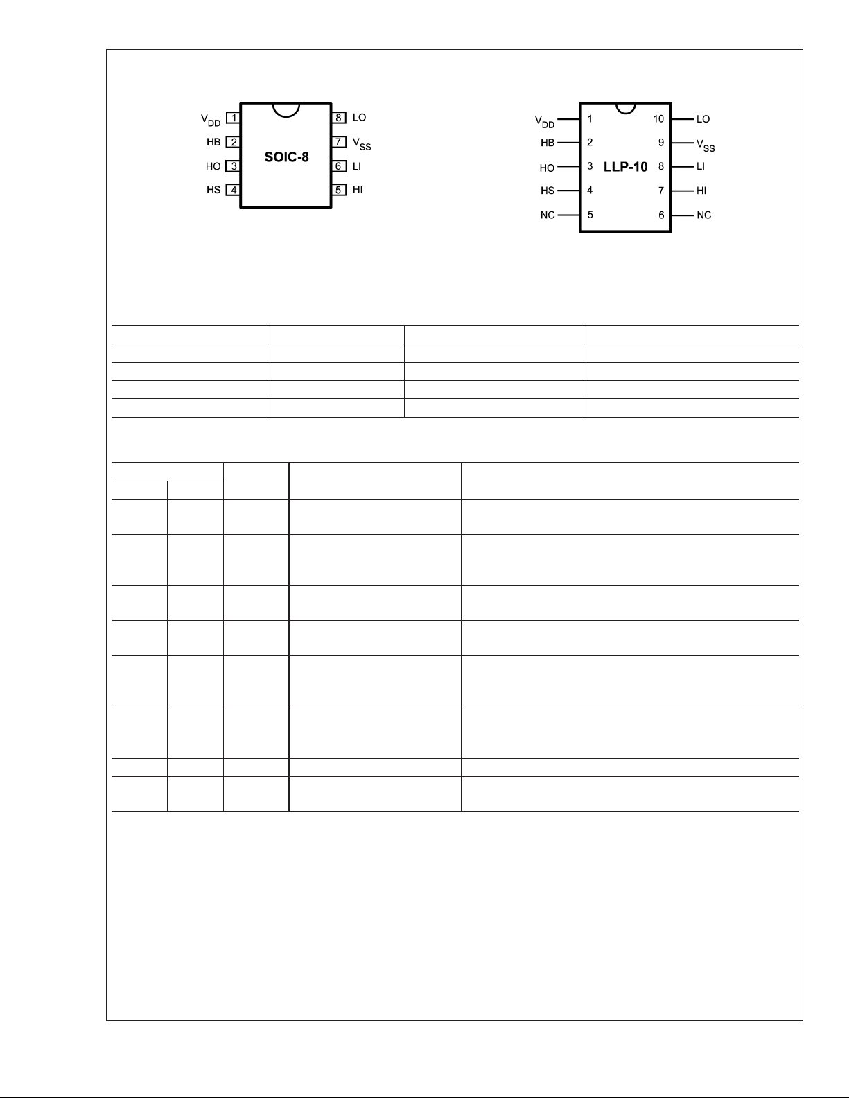
Connection Diagrams
LM5100A/LM5101A
20124001
20124002
FIGURE 2.
Ordering Information
Ordering Number Package Type NSC Package Drawing Supplied As
LM5100A/01A M SOIC-8 M08A Shipped in anti static rails
LM5100A/01A MX SOIC-8 M08A 2500 shipped as Tape & Reel
LM5100A/01A SD LLP-10 SDC10A 1000 shipped as Tape & Reel
LM5100A/01A SDX LLP-10 SDC10A 4500 shipped as Tape & Reel
Pin Description
Pin #
SO-8 LLP-10
11V
2 2 HB High side gate driver
3 3 HO High side gate driver output Connect to gate of high side MOSFET with a short low
4 4 HS High side MOSFET source
5 7 HI High side driver control input The LM5100A inputs have CMOS type thresholds. The
6 8 LI Low side driver control input The LM5100A inputs have CMOS type thresholds. The
79V
8 10 LO Low side gate driver output Connect to the gate of the low side MOSFET with a short low
Note: For LLP-10 package, it is recommended that the exposed pad on the bottom of the LM5100A / LM5101A be soldered to ground plane on the PC
board, and the ground plane should extend out from beneath the IC to help dissipate the heat. Pins 5 and 6 have no connection.
Name Description Application Information
DD
Positive gate drive supply Locally decouple to VSSusing low ESR/ESL capacitor located
as close to IC as possible.
Connect the positive terminal of the bootstrap capacitor to HB
bootstrap rail
and the negative terminal to HS. The Bootstrap capacitor
should be place as close to IC as possible.
inductance path.
Connect to bootstrap capacitor negative terminal and the
connection
source of the high side MOSFET.
LM5101A inputs have TTL type thresholds. Unused inputs
should be tied to ground and not left open.
LM5101A inputs have TTL type thresholds. Unused inputs
should be tied to ground and not left open.
SS
Ground return All signals are referenced to this ground.
inductance path.
www.national.com 2
LM5100A/LM5101A
Absolute Maximum Ratings (Note 1)
If Military/Aerospace specified devices are required,
Storage Temperature Range −55˚C to +150˚C
ESD Rating HBM (Note 2) 2 KV
please contact the National Semiconductor Sales Office/
Distributors for availability and specifications.
Recommended Operating
to V
V
DD
SS
V
to V
HB
HS
LI or HI Inputs −0.3V to V
LO Output −0.3V to V
HO Output V
V
to V
HS
SS
V
to V
HB
SS
HS
Junction Temperature +150˚C
−0.3V to +18V
−0.3V to +18V
+0.3V
DD
+0.3V
DD
−0.3V to VHB+0.3V
−1V to +100V
118V
Conditions
V
DD
HS −1V to 100V
HB V
HS Slew Rate
Junction Temperature −40˚C to +125˚C
+9V to +14V
+8V to VHS+14V
HS
<
50 V/ns
Electrical Characteristics
Specifications in standard typeface are for TJ= +25˚C, and those in boldface type apply over the full operating junction temperature range. Unless otherwise specified, V
DD=VHB
Symbol Parameter Conditions Min Typ Max Units
SUPPLY CURRENTS
I
DD
I
DDO
I
HB
I
HBO
I
HBS
I
HBSO
VDDQuiescent Current LI = HI = 0V (LM5100A) 0.1 0.2
VDDOperating Current f = 500 kHz 2.0 3 mA
Total HB Quiescent Current LI = HI = 0V 0.06 0.2 mA
Total HB Operating Current f = 500 kHz 1.6 3 mA
HB to VSSCurrent, Quiescent VHS=VHB= 100V 0.1 10 µA
HB to VSSCurrent, Operating f = 500 kHz 0.4 mA
INPUT PINS
V
IL
V
IL
V
IHYS
V
IHYS
R
I
Input Voltage Threshold (LM5100A) Rising Edge 4.5 5.4 6.3 V
Input Voltage Threshold (LM5101A) Rising Edge 1.3 1.8 2.3 V
Input Voltage Hysteresis (LM5101A) 50 mV
Input Voltage Hysteresis (LM5100A) 500 mV
Input Pulldown Resistance 100 200 400 kΩ
UNDER VOLTAGE PROTECTION
V
DDR
V
DDH
V
HBR
V
HBH
VDDRising Threshold 6.0 6.8 7.4 V
VDDThreshold Hysteresis 0.5 V
HB Rising Threshold 5.7 6.6 7.1 V
HB Threshold Hysteresis 0.4 V
BOOT STRAP DIODE
V
DL
V
DH
R
D
Low-Current Forward Voltage I
High-Current Forward Voltage I
Dynamic Resistance I
LO GATE DRIVER
V
V
I
I
OLL
OHL
OHL
OLL
Low-Level Output Voltage ILO= 100 mA 0.12 0.25 V
High-Level Output Voltage ILO= −100 mA,
Peak Pullup Current VLO= 0V 3.0 A
Peak Pulldown Current VLO= 12V 3.0 A
HO GATE DRIVER
V
V
I
I
OLH
OHH
OHH
OLH
Low-Level Output Voltage IHO= 100 mA 0.12 0.25 V
High-Level Output Voltage IHO= −100 mA
Peak Pullup Current VHO= 0V 3.0 A
Peak Pulldown Current VHO= 12V 3.0 A
= 12V, VSS=VHS= 0V, No Load on LO or HO .
LI = HI = 0V (LM5101A) 0.25 0.4
= 100 µA 0.52 0.85 V
VDD-HB
= 100 mA 0.80 1.0 V
VDD-HB
= 100 mA 1.0 1.65 Ω
VDD-HB
V
OHL=VDD–VLO
V
OHH=VHB–VHO
0.24 0.45 V
0.24 0.45 V
mA
www.national.com3
Electrical Characteristics (Continued)
Specifications in standard typeface are for TJ= +25˚C, and those in boldface type apply over the full operating junction temperature range. Unless otherwise specified, V
DD=VHB
= 12V, VSS=VHS= 0V, No Load on LO or HO .
Symbol Parameter Conditions Min Typ Max Units
HO GATE DRIVER
THERMAL RESISTANCE
LM5100A/LM5101A
θ
JA
Junction to Ambient SOIC-8 170
LLP-10 (Note 3) 40
Switching Characteristics
Specifications in standard typeface are for TJ= +25˚C, and those in boldface type apply over the full operating junction temperature range. Unless otherwise specified, V
DD=VHB
Symbol Parameter Conditions Min Typ Max Units
LM5100A
t
LPHL
Lower Turn-Off Propagation Delay (LI
Falling to LO Falling)
t
HPHL
Upper Turn-Off Propagation Delay (HI
Falling to HO Falling)
t
LPLH
Lower Turn-On Propagation Delay (LI
Rising to LO Rising)
t
HPLH
Upper Turn-On Propagation Delay (HI
Rising to HO Rising)
t
MON
Delay Matching: Lower Turn-On and
Upper Turn-Off
t
MOFF
Delay Matching: Lower Turn-Off and
Upper Turn-On
t
RC,tFC
t
R,tF
Either Output Rise/Fall Time CL= 1000 pF 8 ns
Either Output Fall Time
(3V to 9V)
Either Output Rise Time
(3V to 9V)
t
PW
Minimum Input Pulse Width that
Changes the Output
t
BS
Bootstrap Diode Turn-Off Time IF= 100 mA,
LM5101A
t
LPHL
Lower Turn-Off Propagation Delay (LI
Falling to LO Falling)
t
HPHL
Upper Turn-Off Propagation Delay (HI
Falling to HO Falling)
t
LPLH
Lower Turn-On Propagation Delay (LI
Rising to LO Rising)
t
HPLH
Upper Turn-On Propagation Delay (HI
Rising to HO Rising)
t
MON
Delay Matching: Lower Turn-On and
Upper Turn-Off
t
MOFF
Delay Matching: Lower Turn-Off and
Upper Turn-On
t
RC,tFC
t
R,tF
Either Output Rise/Fall Time CL= 1000 pF 8 ns
Either Output Fall Time
(3V to 9V)
Either Output Rise Time
(3V to 9V)
= 12V, VSS=VHS= 0V, No Load on LO or HO.
CL= 0.1 µF
CL= 0.1 µF
= 100 mA
I
R
CL= 0.1 µF
CL= 0.1 µF
20 45 ns
20 45 ns
20 45 ns
20 45 ns
1 10 ns
1 10 ns
0.26
0.43
50 ns
38 ns
22 56 ns
22 56 ns
26 56 ns
26 56 ns
4 10 ns
4 10 ns
0.26
0.43
˚C/W
µs
µs
www.national.com 4

Switching Characteristics (Continued)
Specifications in standard typeface are for TJ= +25˚C, and those in boldface type apply over the full operating junction temperature range. Unless otherwise specified, V
DD=VHB
Symbol Parameter Conditions Min Typ Max Units
LM5101A
t
PW
Minimum Input Pulse Width that
Changes the Output
t
BS
Note 1: Absolute Maximum Ratings indicate limits beyond which damage to the component may occur. Operating Ratings are conditions under which operation of
the device is guaranteed. Operating Ratings do not imply guaranteed performance limits. For guaranteed performance limits and associated test conditions, see the
Electrical Characteristics tables.
Note 2: The human body model is a 100 pF capacitor discharged through a 1.5kΩ resistor into each pin. 2 KV for all pins except Pin 2, Pin 3 and Pin 4 which are
rated at 1000V.
Note 3: 4 layer board with Cu finished thickness 1.5/1/1/1.5 oz. Maximum die size used. 5x body length of Cu trace on PCB top. 50 x 50mm ground and power
planes embedded in PCB. See Application Note AN-1187.
Note 4: Min and Max limits are 100% production tested at 25˚C. Limits over the operating temperature range are guaranteed through correlation using Statistical
Quality Control (SQC) methods. Limits are used to calculate National’s Average Outgoing Quality Level (AOQL).
Note 5: The θ
Bootstrap Diode Turn-Off Time IF= 100 mA,
is not a given constant for the package and depends on the printed circuit board design and the operating environment.
JA
= 12V, VSS=VHS= 0V, No Load on LO or HO.
= 100 mA
I
R
50 ns
38 ns
LM5100A/LM5101A
www.national.com5

Typical performance Characteristics
LM5100A IDDvs Frequency LM5101A IDDvs Frequency
LM5100A/LM5101A
20124009 20124010
LM5100A/LM5101A Operating Current vs Temperature IHB vs Frequency
20124011
Quiescent Current vs Supply Voltage LM5100A/LM5101A Quiescent Current vs Temperature
20124018
www.national.com 6
20124014
20124019

Typical performance Characteristics (Continued)
LM5100A Undervoltage Threshold Hysteresis vs
Undervoltage Rising Thresholds vs Temperature
LM5100A/LM5101A
Temperature
20124022
Bootstrap Diode Forward Voltage HO and LO Peak Output Current vs Output Voltage
20124015
LO and HO Gate Drive — High Level Output Voltage vs
Temperature
20124017
20124016
LO and HO Gate Drive — Low Level Output Voltage vs
Temperature
20124020
20124021
www.national.com7

Typical performance Characteristics (Continued)
LM5100A Propagation Delay vs Temperature LM5101A Propagation Delay vs Temperature
LM5100A/LM5101A
20124012
20124013
LM5100A Input Threshold vs Temperature LM5101A Input Threshold vs Temperature
20124023 20124024
LM5100A Input Threshold vs V
DD
LM5101A Input Threshold vs V
DD
20124025 20124026
www.national.com 8

Timing Diagram
LM5100A/LM5101A
20124004
FIGURE 3.
Layout Considerations
The optimum performance of high and low side gate drivers
cannot be achieved without taking due considerations during
circuit board layout. Following points are emphasized.
1. A low ESR / ESL capacitor must be connected close to
the IC, and between V
and VSSpins and between HB
DD
and HS pins to support high peak currents being drawn
from VDD during turn-on of the external MOSFET.
2. To prevent large voltage transients at the drain of the top
MOSFET, a low ESR electrolytic capacitor must be connected between MOSFET drain and ground (V
).
SS
3. In order to avoid large negative transients on the switch
node (HS) pin, the parasitic inductances in the source of
top MOSFET and in the drain of the bottom MOSFET
(synchronous rectifier) must be minimized.
4. Grounding Considerations:
a) The first priority in designing grounding connections
is to confine the high peak currents from charging and
discharging the MOSFET gate in a minimal physical
area. This will decrease the loop inductance and minimize noise issues on the gate terminal of the MOSFET.
The MOSFETs should be placed as close as possible to
the gate driver.
b) The second high current path includes the bootstrap capacitor, the bootstrap diode, the local ground
referenced bypass capacitor and low side MOSFET
body diode. The bootstrap capacitor is recharged on the
cycle-by-cycle basis through the bootstrap diode from
the ground referenced V
bypass capacitor. The re-
DD
charging occurs in a short time interval and involves high
peak current. Minimizing this loop length and area on the
circuit board is important to ensure reliable operation.
Power Dissipation Considerations
The total IC power dissipation is the sum of the gate driver
losses and the bootstrap diode losses. The gate driver
losses are related to the switching frequency (f), output load
capacitance on LO and HO (C
), and supply voltage (VDD)
L
and can be roughly calculated as:
P
DGATES
=2•f•C
2
V
•
L
DD
There are some additional losses in the gate drivers due to
the internal CMOS stages used to buffer the LO and HO
outputs. The following plot shows the measured gate driver
power dissipation versus frequency and load capacitance.At
higher frequencies and load capacitance values, the power
dissipation is dominated by the power losses driving the
output loads and agrees well with the above equation. This
plot can be used to approximate the power losses due to the
gate drivers.
Gate Driver Power Dissipation (LO + HO)
= 12V, Neglecting Diode Losses
V
DD
20124005
The bootstrap diode power loss is the sum of the forward
bias power loss that occurs while charging the bootstrap
capacitor and the reverse bias power loss that occurs during
reverse recovery. Since each of these events happens once
per cycle, the diode power loss is proportional to frequency.
www.national.com9

Power Dissipation Considerations
(Continued)
Larger capacitive loads require more current to recharge the
bootstrap capacitor resulting in more losses. Higher input
voltages (V
recovery losses. The following plot was generated based on
calculations and lab measurements of the diode recovery
LM5100A/LM5101A
time and current under several operating conditions. This
can be useful for approximating the diode power dissipation.
The total IC power dissipation can be estimated from the
previous plots by summing the gate drive losses with the
bootstrap diode losses for the intended application.
) to the half bridge result in higher reverse
IN
Diode Power Dissipation V
IN
= 50V
20124006
www.national.com 10

Physical Dimensions inches (millimeters) unless otherwise noted
LM5100A/LM5101A
Controlling dimension is inch. Values in [ ] are millimeters.
Notes: Unless otherwise specified.
1. Standard lead finish to be 200 microinches/5.08 micrometers minimum lead/tin (solder) on copper.
2. Dimension does not include mold flash.
3. Reference JEDEC registration MS-012, Variation AA, dated May 1990.
SOIC-8 Outline Drawing
NS Package Number M08A
www.national.com11

Physical Dimensions inches (millimeters) unless otherwise noted (Continued)
Notes: Unless otherwise specified.
1. For solder thickness and composition, see “Solder Information” in the packaging section of the National Semiconductor web
page (www.national.com).
2. Maximum allowable metal burr on lead tips at the package edges is 76 microns.
3. No JEDEC registration as of May 2003.
LLP-10 Outline Drawing
NS Package Number SDC10A
National does not assume any responsibility for use of any circuitry described, no circuit patent licenses are implied and National reserves
the right at any time without notice to change said circuitry and specifications.
For the most current product information visit us at www.national.com.
LIFE SUPPORT POLICY
NATIONAL’S PRODUCTS ARE NOT AUTHORIZED FOR USE AS CRITICAL COMPONENTS IN LIFE SUPPORT DEVICES OR SYSTEMS
LM5100A/LM5101A 3.0 Amp High Voltage High Side and Low Side Driver
WITHOUT THE EXPRESS WRITTEN APPROVAL OF THE PRESIDENT AND GENERAL COUNSEL OF NATIONAL SEMICONDUCTOR
CORPORATION. As used herein:
1. Life support devices or systems are devices or systems
which, (a) are intended for surgical implant into the body, or
(b) support or sustain life, and whose failure to perform when
properly used in accordance with instructions for use
2. A critical component is any component of a life support
device or system whose failure to perform can be reasonably
expected to cause the failure of the life support device or
system, or to affect its safety or effectiveness.
provided in the labeling, can be reasonably expected to result
in a significant injury to the user.
BANNED SUBSTANCE COMPLIANCE
National Semiconductor manufactures products and uses packing materials that meet the provisions of the Customer Products
Stewardship Specification (CSP-9-111C2) and the Banned Substances and Materials of Interest Specification (CSP-9-111S2) and contain
no ‘‘Banned Substances’’ as defined in CSP-9-111S2.
National Semiconductor
Americas Customer
Support Center
Email: new.feedback@nsc.com
Tel: 1-800-272-9959
www.national.com
National Semiconductor
Europe Customer Support Center
Fax: +49 (0) 180-530 85 86
Email: europe.support@nsc.com
Deutsch Tel: +49 (0) 69 9508 6208
English Tel: +44 (0) 870 24 0 2171
Français Tel: +33 (0) 1 41 91 8790
National Semiconductor
Asia Pacific Customer
Support Center
Email: ap.support@nsc.com
National Semiconductor
Japan Customer Support Center
Fax: 81-3-5639-7507
Email: jpn.feedback@nsc.com
Tel: 81-3-5639-7560
 Loading...