

April 2006
LM5071
Power Over Ethernet PD Controller with Auxiliary Power
Interface
General Description
The LM5071 power interface port and pulse width modulation (PWM) controller provides a complete integrated solution for Powered Devices (PD) that connect into Power over
Ethernet (PoE) systems. The LM5071 is specifically de-
signed for the PD that must accept power from auxiliary
sources such as ac adapters. The auxiliary power inter-
face of the LM5071 activates the PWM controller when the
ac adapter is connected to power the PD when PoE network
power is unavailable. The LM5071 integrates an 80V,
400mA line connection switch and associated control for a
fully IEEE 802.3af compliant interface with a full featured
current mode pulse width modulator dc-dc converter. All
power sequencing requirements between the controller interface and switch mode power supply (SMPS) are integrated into the IC.
n Detection Resistor Disconnect Function
n Programmable Classification Current
n Programmable Under-voltage Lockout with
Programmable Hysteresis
n Thermal Shutdown Protection
n Auxiliary Power Enable Pin
n Current Mode Pulse Width Modulator
n Supports both Isolated and Non-Isolated Applications
n Error Amplifier and Reference for Non-Isolated
Applications
n Programmable Oscillator Frequency
n Programmable Soft-start
n 80% Maximum Duty Cycle Limiter, Slope Compensation
(-80 device)
n 50% Maximum Duty Cycle Limiter, No Slope
Compensation (-50 device)
LM5071 Power Over Ethernet PD Controller with Auxiliary Power Interface
Features
n Compatible with 12V ac adapters
n Fully Compliant 802.3af Power Interface Port
n 80V, 1Ω, 400 mA Internal MOSFET
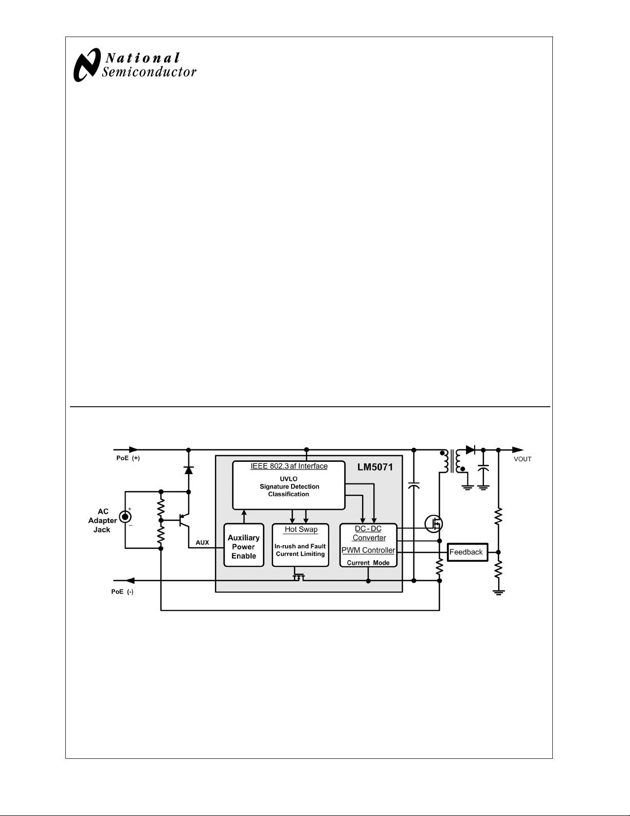
Block Diagram
Packages
n TSSOP-16
20168401
© 2006 National Semiconductor Corporation DS201684 www.national.com
Block Diagram (Continued)
LM5071
20168402
FIGURE 1. Simplified Block Diagram
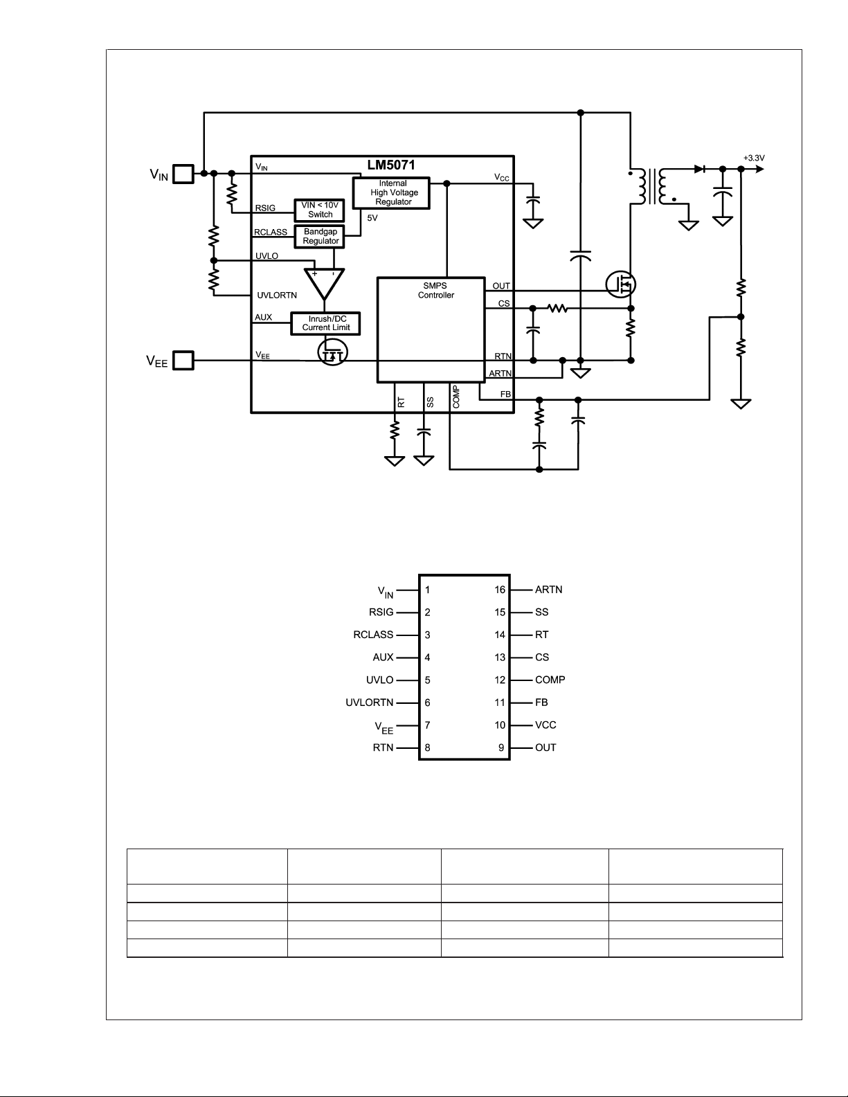
Connection Diagram
16 Lead TSSOP
20168403
Ordering Information
NSC Package Type /
Order Number Description
LM5071MT-50 50% Duty Cycle Limit TSSOP-16/MTC-16 92 units per rail
LM5071MTX-50 50% Duty Cycle Limit TSSOP-16/MTC-16 2500 units on tape and reel
LM5071MT-80 80% Duty Cycle Limit TSSOP-16/MTC-16 92 units per rail
LM5071MTX-80 80% Duty Cycle Limit TSSOP-16/MTC-16 2500 units on tape and reel
Drawing Supplied As
www.national.com 2

Pin Descriptions
Pin Name Description Application Information
1 VIN System high potential input. The diode “OR” of several lines entering the PD, it is the more
positive input potential.
2 RSIG Signature resistor pin. Connect a resistor from V
resistor is in parallel with the UVLO resistors and should be valued
accordingly.
3 RCLASS Classification resistor pin. Connect the classification programming resistor from this pin to V
4 AUX Auxiliary input power startup pin. A resistor divider between the AUX voltage input to VEE programs
the startup levels with a 2.5V threshold. A high value (>300kΩ)
internal pull down resistor is present to pull the pin low if it is left
open. In practice, the divider voltage should be set well above 2.5V
by the programming resistors.
5 UVLO Line under-voltage lockout. An external resistor divider from V
shutdown levels with a 2.00V threshold at the UVLO pin. Hysteresis
is set by a switched internal 10uA current source that forces
additional current into the resistor divider.
6 UVLORTN Return for the external UVLO resistors. Connect the bottom resistor of the resistor divider between the
UVLO pin and this pin.
7 VEE System low potential input. Diode “OR’d” to the RJ45 connector and PSE’s –48V supply, it is
the more negative input potential.
8 RTN System return for the PWM converter. The drain of the internal current limiting power MOSFET which
connects V
to the return path of the dc-dc converter.
EE
9 OUT Output of the PWM controller. DC-DC converter gate driver output with 800mA peak sink current
capability.
10 V
Output of the internal high voltage
CC
series pass regulator. Regulated output
voltage is nominally 7.8V.
When the auxiliary transformer winding (if used) raises the voltage
on this pin above the regulation set point, the internal series pass
regulator will shutdown, reducing the controller power dissipation.
11 FB Feedback signal. Inverting input of the internal error amplifier. The non-inverting input
is internally connected to a 1.25V reference.
12 COMP The output of the error amplifier and
input to the Pulse Width Modulator.
COMP pull-up is provided by an internal 5K resistor which may be
used to bias an opto-coupler transistor.
13 CS Current sense input. Current sense input for current mode control and over-current
protection. Current limiting is accomplished using a dedicated
current sense comparator. If the CS pin voltage exceeds 0.5V the
OUT pin switches low for cycle-by-cycle current limiting. CS is held
low for 50ns after OUT switches high to blank leading edge current
spikes.
14 RT / SYNC Oscillator timing resistor pin and
synchronization input.
An external resistor connected from RT to ARTN sets the oscillator
frequency. This pin will also accept narrow ac-coupled
synchronization pulses from an external clock.
15 SS Soft-start input. An external capacitor and an internal 10uA current source set the
soft-start ramp rate.
16 ARTN Analog PWM supply return. RTN for sensitive analog circuitry including the SMPS current limit
amplifier.
to this pin for signature detection. The
IN
to UVLORTN programs the
IN
EE
LM5071
.
www.national.com3
Absolute Maximum Ratings (Note 1)
If Military/Aerospace specified devices are required,
LM5071
please contact the National Semiconductor Sales Office/
Distributors for availability and specifications.
,RTN to V
V
IN
RSIG to V
AUX to V
UVLO to V
RCLASS to V
ARTN to RTN -0.3V to 0.3V
V
, OUT to ARTN -0.3V to 16V
CC
All other inputs to ARTN -0.3V to 7V
EE
IN
EE
EE
EE
-0.3V to 80V
-12V to 0V
-0.3V to 57V
-0.3V to 13V
-0.3V to 7V
ESD Rating
Human Body Model 2000V
Lead Temperature (Note 2)
Wave (4 seconds)
Infrared (10 seconds)
Vapor Phase (75 seconds)
Operating Ratings
VINvoltage 1.8V to 60V
External voltage applied to V
CC
Operating Junction Temperature -40˚C to 125˚C
8.1V to 15V
Electrical Characteristics (Note 3)
Specifications in standard type face are for TJ= +25˚C and those in boldface type apply over the full operating junction temperature range. Unless otherwise specified: V
Symbol Parameter Conditions Min Typ Max Units
Powered Interface
IOS Offset Current V
VCLSS(ON) Signature Resistor Disable /
Classification Current Turn On
VCLSS(OFF) Classification Current Turn Off VINwith respect to V
Classification Voltage With respect to V
ICLASS Supply Current During
Classification
IDC Supply Current During Normal
Operation
UVLO Pin Reference Voltage V
UVLO Hysteresis Current V
Softstart Release RTN falling with respect to V
Softstart Release Hysteresis RTN rising with respect to V
RDS(ON) PowerFET Resistance I = 350mA,
ILEAK SMPS Bias Current V
AUX Pin Threshold AUX pin rising with respect to
AUX Pin Threshold Hysteresis AUX pin falling with respect to
ZAUX AUX Pin Input Impedance AUX = 0.5V 350 kΩ
I
INRUSH
Inrush Current Limit VEE= 0V, RTN = 3.0V 70 100 130 mA
ILIM DC Current Limit V
ILIM DC Current Limit VEE= 0V, RTN = 3.0V,
Startup Regulator
VinMin Operational VIN Input Voltage AUX = 5V, Vcc = Vin (Note 6) 9.5 V
VccReg V
Regulation Open ckt 7.5 7.8 8.1 V
CC
V
Current Limit (Note 4) 15 20 mA
CC
= 48V, VCC= 10V, RT = 30.3kΩ.
IN
<
10.0V 10 uA
IN
V
with respect to V
IN
V
=17V 0.5 1.0 mA
IN
EE
EE
EE
10.0 11.5 12.5 V
23.5 25.0 26.5 V
1.43 1.5 1.57 V
OUT floating 1 1.9 mA
>
27V 1.95 2.00 2.05 V
IN
>
UVLO 8.0 10 11.5 uA
IN
EE
EE
1.2 1.45 1.7 V
0.8 1.1 1.3 V
1 2.2 Ω
VIN= 48V
= 0V, VIN= RTN = 57V 100 uA
EE
2.4 2.5 2.65 V
V
EE
0.4 0.5 0.6 V
V
EE
= 0V, RTN = 3.0V,
EE
350 390 420 mA
Temp = 0˚C to 85˚C
325 390 420 mA
Temp = -40˚C to 125˚C
260˚C
240˚C
219˚C
www.national.com 4
Electrical Characteristics (Note 3) (Continued)
Specifications in standard type face are for TJ= +25˚C and those in boldface type apply over the full operating junction temperature range. Unless otherwise specified: V
Symbol Parameter Conditions Min Typ Max Units
V
Supply
CC
V
UVLO (Rising) VccReg
CC
UVLO (Falling) 5.9 6.25 6.6 V
V
CC
Supply Current (Icc) Cload = 0 1.5 3 mA
Error Amplifier
GBW Gain Bandwidth 4 MHz
DC Gain 75 dB
Input Voltage FB = COMP 1.219
COMP Sink Capability FB=1.5V COMP=1V 5 20 mA
Current Limit
ILIM Delay to Output CS step from 0 to 0.6V, time to
Cycle by Cycle Current Limit
Threshold Voltage
Leading Edge Blanking Time 55 ns
CS Sink Impedance (clocked) 25 55 Ω
Softstart
Softstart Current Source 7 10 13 uA
Oscillator(Note 5)
Frequency1
(RT = 30.3K)
Frequency2
(RT = 10.5K)
Sync threshold 3.1 3.8 V
PWM Comparator
Delay to Output COMP set to 2V
Min Duty Cycle COMP=0V 0 %
Max Duty Cycle (-80 Device) 80 %
Max Duty Cycle (-50 Device) 50 %
COMP to PWM Comparator
Gain
COMP Open Circuit Voltage 4.5 5.4 6.3 V
COMP Short Circuit Current COMP= 0V 0.6 1.1 1.5 mA
Slope Compensation
Slope Comp Amplitude
(LM5071-80 Device Only)
Output Section
Output High Saturation I
Output Low Saturation I
Rise time Cload = 1nF 15 ns
Fall time Cload = 1nF 15 ns
= 48V, VCC= 10V, RT = 30.3kΩ.
IN
onset of OUT transition (90%)
CS stepped 0 to 0.4V, time to
onset of OUT transition low
Delta increase at PWM
Comparator to CS
= 50mA,
out
V
CC-VOUT
= 100mA 0.25 0.75 V
out
VccReg –
–
100mV
300mV
1.281
1.212
1.288
20 ns
0.44 0.5 0.56 V
175 200 225 KHz
505 580 665 KHz
25 ns
0.33
105 mV
0.25 0.75 V
V
LM5071
www.national.com5

Electrical Characteristics (Note 3) (Continued)
Specifications in standard type face are for TJ= +25˚C and those in boldface type apply over the full operating junction tem-
LM5071
perature range. Unless otherwise specified: V
Symbol Parameter Conditions Min Typ Max Units
Thermal Shutdown
Tsd Thermal Shutdown Temp. 165 ˚C
Thermal Shutdown
Hysteresis
Thermal Resistance
θ
JA
Note 1: Absolute Maximum Ratings are limits beyond which damage to the device may occur. Operating Ratings are conditions under which operation of the device
is intended to be functional. For guaranteed specifications and test conditions, see the Electrical Characteristics. The absolute maximum rating ofV
is derated to (-0.3V to 76V) at -40˚C.
Note 2: For detailed information on soldering the plastic TSSOP package, refer to the Packaging Databook available from National Semiconductor.
Note 3: Min and Max limits are 100% production tested at 25 ˚C. Limits over the operating temperature range are guaranteed through correlation using Statistical
Quality Control (SQC) methods. Limits are used to calculate National’s Average Outgoing Quality Level (AOQL).
Note 4: Device thermal limitations may limit usable range.
Note 5: Specification applies to the oscillator frequency. The operational frequency of the LM5071-50 devices is divided by two.
Note 6: The Vcc regulator requires an external source whenever the Vin pin is below 13V with respect to RTN.An external load on Vcc increases this startup voltage
requirement.
Junction to Ambient MT Package 125 ˚C/W
= 48V, VCC= 10V, RT = 30.3kΩ.
IN
25 ˚C
IN
, RTN to V
EE
www.national.com 6

Typical Performance Characteristics
Default Current Limit vs Temperature Oscillator Frequency vs RT Resistance
LM5071
20168409
UVLO Hysteresis Current vs Temperature Softstart Current vs Temperature
20168408 20168415
Oscillator Frequency vs Temperature
Error Amp Input Voltage vs temperature
RT = 15.2 kΩ
20168413
20168417 20168414
www.national.com7

Typical Performance Characteristics (Continued)
LM5071
V
vs I
CC
CC
UVLO Threshold vs Temperature
20168412
Input Current vs Input Voltage
20168407
20168406
www.national.com 8

Specialized Block Diagrams
LM5071
FIGURE 2. Top Level Block Diagram
20168404
FIGURE 3. PWM Controller Block Diagram
20168405
www.national.com9

Detailed Operating Description
The LM5071 power interface port and pulse width modula-
LM5071
tion (PWM) controller provides a complete integrated solution for Powered Devices (PD) that connect into Power over
Ethernet (PoE) systems. Major features of the PD interface
portion of the IC include detection, classification, thermal
limit, programmable undervoltage lockout, and current limit
monitoring. The device also includes a high-voltage start-up
bias regulator that operates over a wide input range up to
60V. The switch mode power supply (SMPS) control portion
of the IC includes power good sensing, V
regulator under-
CC
voltage lockout, cycle-by-cycle current limit, error amplifier,
slope compensation, softstart, and oscillator sync capability.
This high speed BiCMOS IC has total propagation delays
less than 100ns and a 1MHz capable oscillator programmed
by a single external resistor. The LM5071 PWM controller
provides current-mode control for dc-dc converter topologies
requiring a single drive output, such as Flyback and Forward
topologies. The LM5071 PWM enables all of the advantages
of current-mode control including line feed-forward, cycle-bycycle current limit and simplified loop compensation. The
oscillator ramp is internally buffered and added to the PWM
comparator input ramp to provide slope compensation necessary for current mode control at duty cycles greater than
50% (-80 suffix only).
Modes of Operation
The LM5071 PD interface is designed to provide a fully
compliant IEEE 802.3af system. As such, the modes of
operation take into account the barrel rectifiers often utilized
to correctly polarize the dc input from the Ethernet cable.
Table 1 shows the LM5071 operating modes and associated
input voltage range.
TABLE 1. Operating Modes With Respect to Input
Voltage
Input Voltage
wrt V
V
IN
EE
1.8V to 10.0V Detection
12.5V to 25.0V Classification
25.0V to UVLO
Rising Vth
60V to UVLO
Falling Vth
An external signature resistor is connected to V
exceeds 1.8V, initiating detection mode. During detection
mode, quiescent current drawn by the LM5071 is less than
10uA. Between 10.0V and 12.5V, the device enters classification mode and the signature resistor is disabled. The
nominal range for classification mode is 11.5V to 25.0V. The
classification current is turned off once the classification
range voltage is exceeded, to reduce power dissipation.
Between 25.0V and UVLO release, the device is in a
standby state, awaiting the input voltage to reach the operational range to complete the power up sequence. Once the
voltage increases above the upper UVLO threshold volt-
V
IN
Mode of
Operation
(Signature)
Awaiting Full
Power
Normal Powered
Operation
EE
when V
age, the internal power MOSFET is enabled to deliver a
constant current to charge the input capacitor of the dc-dc
converter. When the MOSFET Vds voltage falls below 1.5V,
the internal Power Good signal enables the SMPS controller.
The LM5071 is specified to operate with an input voltage as
high as 60.0V. The SMPS controller and internal MOSFET
are disabled when V
falls to the lower UVLO threshold.
IN
Detection Signature
To detect a potential powered device candidate, the PSE
(Power Sourcing Equipment) will apply a voltage from 2.8V
to 10V across the input terminals of the PD. The voltage can
be of either polarity so a diode barrel network is required on
both lines to ensure this capability. The PSE will take two
measurements, separated by at least 1V and 2ms of time.
The voltage ramp between measurement points will not
exceed 0.1V/us. The delta voltage / delta current calculation
is then performed; if the detected impedance is above
23.75kΩ and below 26.25kΩ, the PSE will consider a PD to
be present. If the impedance is less than 15kΩ or greater
than 33kΩ a PD will be considered not present and will not
receive power. Impedances between these values may or
may not indicate the presence of a valid PD. The LM5071
will enable the signature resistor at a controller input voltage
of 1.5V to take into account the diode voltage drops. An
external signature resistor should be placed between the
VIN and RSIG pins. The signature resistor is in parallel with
the external UVLO resistor divider, and its value should be
calculated accordingly. Targeting 24.5kΩ increases margin in
the signature design as the input bridge rectifier diodes
contribute to the series resistance measured at the PD input
terminals. The PSE will tolerate no more than 1.9V of offset
voltage (caused by the external diodes) or more than 10uA
of offset current (bias current). The input capacitance must
be greater than 0.05uF and less than 0.12uF. To increase
efficiency, the signature resistor is disabled by the LM5071
controller once the input voltage is above the detection
>
range (
11V).
Classification
To classify the PD, the PSE will present a voltage between
14.5V and 20.5V to the PD. The LM5071 enables classification mode at a nominal input voltage of 11.5V. An internal
1.5V linear regulator and an external resistor connected to
the RCLASS pin provide classification programming current.
Table 2 shows the external classification resistor required for
a particular class.
The classification current flows through the IC into the clas-
IN
sification resistor. The suggested resistor values take into
account the bias current flowing into the IC. A different
desired RCLASS can be calculated by dividing 1.5V by the
desired classification current.
Per the IEEE 802.3af specification, classification is optional,
and the PSE will default to class 0 if a valid classification
current is not detected. If PD classification is not desired
(i.e., Class 0), simply leave the RCLASS pin open. The
classification time period may not last longer than 75ms as
per IEEE 802.3af. The LM5071 will remain in classification
mode until V
is greater than 25V.
IN
www.national.com 10

Classification (Continued)
TABLE 2. Classification Levels and Required External
Resistors
Class PMIN PMAX ICLASS
(MIN)
0 0.44W 12.95W 0mA 4mA Open
1 0.44W 3.84W 9mA 12mA 150Ω
2 3.84W 6.49W 17mA 20mA 82.5Ω
3 6.49W 12.95W 26mA 30mA 54.9Ω
4 Reserved Reserved 36mA 44mA 38.3Ω
ICLASS
(MAX)
RCLASS
LM5071
of the UVLO set point divider. When the UVLO threshold is
exceeded, the current source is activated to instantly raise
the voltage at the UVLO pin. When the UVLO pin voltage
falls below the 2.00V threshold, the current source is turned
off, causing the voltage at the UVLO pin to fall. The LM5071
UVLO thresholds cannot be programmed lower than 25V,
the AUX pin should be used to force UVLO release below
25V.
There are many additional uses for the UVLO pin. The UVLO
function can also be used to implement a remote enable /
disable function. Pulling the UVLO pin down below the
UVLO threshold disables the interface and SMPS controller
unless forced on via AUX pin operation.
Undervoltage Lockout (UVLO)
The IEEE 802.3af specification states that the PSE will
supply power to the PD within 400ms after completion of
detection. The LM5071 contains a programmable line Under
Voltage Lock Out (UVLO) circuit. The first resistor should be
connected between the V
tor in the divider should be connected between the UVLO
and UVLORTN pins.
The divider must be designed such that the voltage at the
UVLO pin equals 2.0V when V
mum operating level. If the UVLO threshold is not met, the
interface control and SMPS control will remain in standby.
UVLO hysteresis is accomplished with an internal 10uA
current source that is switched on and off into the impedance
to UVLO pins; the bottom resis-
IN
reaches the desired mini-
IN
AUX Pin Operation
The AUX pin can be used to force operation (UVLO release)
of the interface and switching regulator at any input voltage
above 9.5V. This is especially useful for auxiliary input (wall
transformer) input voltages. The pin has a 2.5V threshold
(0.5V hysteresis) and an input impedance of approximately
350kΩ. The input resistor provides a defined pull down
impedance if the pin is left open by the user. An external pull
down resistor should be used to provide additional noise
immunity. The resultant pin voltage from the external resistor
divider should be well above the 2.5V threshold to ensure
proper auxiliary operation. See Figure 4 for an example of a
simple yet robust auxiliary configuration.
FIGURE 4. Simplified Schematic Showing Auxiliary Implementation
20168422
www.national.com11

Power Supply Operation
Once the UVLO threshold has been satisfied, the interface
LM5071
controller of the LM5071 will charge up the SMPS input
capacitor through the internal power MOSFET. This load
capacitance provides input filtering for the power converter
section and must be at least 5uF per the IEEE 802.3af
specification. To accomplish the charging in a controlled
manner, the power MOSFET is current limited to 100mA.
The SMPS controller will not initiate operation until the load
capacitor is completely charged. The power sequencing between the interface circuitry and the SMPS controller occurs
automatically within the LM5071. Detection circuitry monitors
the RTN pin to detect interface startup completion. When the
RTN pin potential drops below 1.5V with respect to V
regulator of the SMPS controller is enabled. The soft-
V
CC
start function is enabled once the V
regulator achieves
CC
minimum operating voltage. The inrush current limit only
applies to the initial charging phase. The interface power
MOSFET current limit will revert to the default protection
current limit of 390mA once the SMPS is powered up and the
soft-start pin sequence begins.
High Voltage Start-up Regulator
The LM5071 contains an internal high voltage startup regulator that allows the input pin (V
line voltages as high as 60V. The regulator output is internally current limited to 15mA. The recommended capaci-
) to be connected directly to
IN
tance range for the V
When the voltage on the V
regulator output is 0.1uF to 10uF.
CC
pin reaches the regulation
CC
point of 7.8V, the controller output is enabled. The controller
will remain enabled until V
falls below 6.25V.
CC
In typical applications, a transformer auxiliary winding is
diode connected to the V
the V
voltage above 8.1V to shut off the internal startup
CC
regulator. Though not required, powering V
pin. This winding should raise
CC
from an aux-
CC
iliary winding improves conversion efficiency while reducing
the power dissipated in the controller. The external V
CC
capacitor must be selected such that the capacitor maintains
the V
voltage greater than the VCCUVLO falling threshold
CC
(6.25V) during the initial start-up. During a fault condition
, the
EE
when the converter auxiliary winding is inactive, external
current draw on the V
line should be limited such that the
CC
power dissipated in the start-up regulator does not exceed
the maximum power dissipation capability of the LM5071
package.
If the V
auxiliary winding is used with a low voltage aux-
CC
iliary supply (wall transformer), the VCC pin could back feed
through the LM5071 to the VIN pin. A diode from VCC to VIN
should be used to clamp the VCC pin and prevent this
internal back feed. The winding voltage will remain the same
and extra power will be dissipated in the series resistor. Also,
note that when using a very low voltage auxiliary supply
<
14V), a diode from the AUX supply to the VCC pin should
(
be used to ensure VCC startup.
FIGURE 5. Simplified Schematic Showing Low Voltage Auxiliary Supply
www.national.com 12
20168423

Error Amplifier
An internal high gain error amplifier is provided within the
LM5071. The amplifier’s non-inverting reference is set to a
fixed reference voltage of 1.25V. The inverting input is connected to the FB pin. In non-isolated applications, the power
converter output is connected to the FB pin via voltage
scaling resistors. Loop compensation components are connected between the COMP and FB pins. For most isolated
applications the error amplifier function is implemented on
the secondary side of the converter and the internal error
amplifier is not used. The internal error amplifier is configured as an open drain output and can be disabled by connecting the FB pin to ARTN. An internal 5K pull-up resistor
between a 5V reference and COMP can be used as the
pull-up for an optocoupler in isolated applications.
Current Limit / Current Sense
The LM5071 provides a cycle-by-cycle over current protection function. Current limit is accomplished by an internal
current sense comparator. If the voltage at the current sense
comparator input CS exceeds 0.5V with respect to RTN/
ARTN, the output pulse will be immediately terminated. A
small RC filter, located near the CS pin of the controller, is
recommended to filter noise from the current sense signal.
The CS input has an internal MOSFET which discharges the
CS pin capacitance at the conclusion of every cycle. The
discharge device remains on an additional 50ns after the
beginning of the new cycle to attenuate the leading edge
spike on the current sense signal.
The LM5071 current sense and PWM comparators are very
fast, and may respond to short duration noise pulses. Layout
considerations are critical for the current sense filter and
sense resistor. The capacitor associated with the CS filter
must be located very close to the device and connected
directly to the pins of the controller (CS and ARTN). If a
current sense transformer is used, both leads of the transformer secondary should be routed to the sense resistor and
the current sense filter network. A sense resistor located in
the source of the primary power MOSFET may be used for
current sensing, but a low inductance resistor is required.
When designing with a current sense resistor, all of the noise
sensitive low power ground connections should be connected together local to the controller and a single connection should be made to the high current power return (sense
resistor ground point).
LM5071
LM5071-50:
The LM5071 can also be synchronized to an external clock.
The external clock must have a higher frequency than the
free running oscillator frequency set by the RT resistor. The
clock signal should be capacitively coupled into the RT pin
with a 100pF capacitor. A peak voltage level greater than 3.7
volts at the RT pin is required for detection of the sync pulse.
The sync pulse width should be set between 15 to 150ns by
the external components. The RT resistor is always required,
whether the oscillator is free running or externally synchronized. The voltage at the RT pin is internally regulated to a 2
volts. The RT resistor should be located very close to the
device and connected directly to the pins of the controller
(RT and ARTN).
PWM Comparator / Slope Compensation
The PWM comparator compares the current ramp signal
with the loop error voltage derived from the error amplifier
output. The error amplifier output voltage at the COMP pin is
offset by 1.4V and then further attenuated by a 3:1 resistor
divider. The PWM comparator polarity is such that 0 Volts on
the COMP pin will result in zero duty cycle at the controller
output. For duty cycles greater than 50 percent, current
mode control circuits are subject to sub-harmonic oscillation.
By adding an additional fixed slope voltage ramp signal
(slope compensation) to the current sense signal, this oscillation can be avoided. The LM5071-80 integrates this slope
compensation by summing a current ramp generated by the
oscillator with the current sense signal. Additional slope
compensation may be added by increasing the source impedance of the current sense signal (with an external resistor between the CS pin and current sense resistor). Since
the LM5071-50 is not capable of duty cycles greater than
50%, there is no slope compensation feature in this device.
Oscillator, Shutdown and Sync Capability
A single external resistor connected between the RT and
ARTN pins sets the LM5071 oscillator frequency. Internal to
the LM5071–50 device (50% duty cycle limited option) is an
oscillator divide by two circuit. This divide by two circuit
creates an exact 50% duty cycle clock which is used internally to create a precise 50% duty cycle limit function. Because of this divide by two, the internal oscillator actually
operates at twice the frequency of the output (OUT). For the
LM5071–80 device the oscillator frequency and the operational output frequency are the same. To set a desired output
operational frequency (F), the RT resistor can be calculated
from:
LM5071-80:
Softstart
The softstart feature allows the power converter to gradually
reach the initial steady state operating point, thereby reducing start-up stresses, output overshoot and current surges.
At power on, after the V
satisfied, an internal 10µA current source charges an external capacitor connected to the SS pin. The capacitor voltage
will ramp up slowly and will limit the COMP pin voltage and
the duty cycle of the output pulses.
undervoltage lockout threshold is
CC
Gate Driver and Maximum Duty Cycle Limit
The LM5071 provides an internal gate driver (OUT), which
can source and sink a peak current of 800mA. The LM5071
is available in two duty cycle limit options. The maximum
output duty cycle is typically 80% for the LM5071-80 option
and precisely equal to 50% for the LM5071-50 option. The
maximum duty cycle function for the LM5071-50 is accom-
www.national.com13

Gate Driver and Maximum Duty
Cycle Limit
LM5071
plished with an internal toggle flip-flop which ensures an
accurate duty cycle limit. The internal oscillator frequency of
the LM5071-50 is therefore twice the operating frequency of
the PWM controller (OUT pin).
The 80% maximum duty cycle limit of the LM5071-80 is
determined by the internal oscillator and varies more than
the 50% limit of the LM5071-50. For the LM5071-80, the
internal oscillator frequency and the operational frequency of
the PWM controller are equal.
(Continued)
Thermal Protection
Internal thermal shutdown circuitry is provided to protect the
integrated circuit in the event the maximum junction tem-
perature is exceeded. This feature prevents catastrophic
failures from accidental device overheating. When activated,
typically at 165 degrees Celsius, the controller is forced into
a low power standby state, disabling the output driver, bias
regulator, main interface pass MOSFET, and classification
regulator if enabled. After the temperature is reduced (typical
hysteresis = 25˚C ) the V
softstart sequence initiated.
Thermal shutdown is not enabled during auxiliary power
operation as the power MOSFET is not running any current
and should not experience an over-temperature condition. If
the drain of the MOSFET exceeds 2.5V with respect to VEE
(internal Power Good de-assertion), PoE UVLO becomes
de-asserted (insertion of PoE or other 48V supply), or the
auxiliary power is removed, thermal limit will be re-enabled
immediately.
regulator will be enabled and a
CC
www.national.com 14

20168424
LM5071
LM5071 Application Circuit Diagrams
FIGURE 6. Single Isolated Output with Diode Rectification and 12V Auxiliary Supply
www.national.com15

LM5071
20168425
LM5071 Application Circuit Diagrams (Continued)
www.national.com 16
FIGURE 7. Dual Isolated Output with Diode Rectification

20168426
LM5071
LM5071 Application Circuit Diagrams (Continued)
FIGURE 8. Non-Isolated Output Buck with Diode Rectification
www.national.com17

Physical Dimensions inches (millimeters) unless otherwise noted
Package Number MTC16
National does not assume any responsibility for use of any circuitry described, no circuit patent licenses are implied and National reserves
the right at any time without notice to change said circuitry and specifications.
For the most current product information visit us at www.national.com.
LIFE SUPPORT POLICY
NATIONAL’S PRODUCTS ARE NOT AUTHORIZED FOR USE AS CRITICAL COMPONENTS IN LIFE SUPPORT DEVICES OR SYSTEMS
WITHOUT THE EXPRESS WRITTEN APPROVAL OF THE PRESIDENT AND GENERAL COUNSEL OF NATIONAL SEMICONDUCTOR
CORPORATION. As used herein:
LM5071 Power Over Ethernet PD Controller with Auxiliary Power Interface
1. Life support devices or systems are devices or systems
which, (a) are intended for surgical implant into the body, or
(b) support or sustain life, and whose failure to perform when
properly used in accordance with instructions for use
2. A critical component is any component of a life support
device or system whose failure to perform can be reasonably
expected to cause the failure of the life support device or
system, or to affect its safety or effectiveness.
provided in the labeling, can be reasonably expected to result
in a significant injury to the user.
BANNED SUBSTANCE COMPLIANCE
National Semiconductor manufactures products and uses packing materials that meet the provisions of the Customer Products
Stewardship Specification (CSP-9-111C2) and the Banned Substances and Materials of Interest Specification (CSP-9-111S2) and contain
no ‘‘Banned Substances’’ as defined in CSP-9-111S2.
Leadfree products are RoHS compliant.
National Semiconductor
Americas Customer
Support Center
Email: new.feedback@nsc.com
Tel: 1-800-272-9959
www.national.com
National Semiconductor
Europe Customer Support Center
Fax: +49 (0) 180-530 85 86
Email: europe.support@nsc.com
Deutsch Tel: +49 (0) 69 9508 6208
English Tel: +44 (0) 870 24 0 2171
Français Tel: +33 (0) 1 41 91 8790
National Semiconductor
Asia Pacific Customer
Support Center
Email: ap.support@nsc.com
National Semiconductor
Japan Customer Support Center
Fax: 81-3-5639-7507
Email: jpn.feedback@nsc.com
Tel: 81-3-5639-7560
 Loading...