

January 2007
LM5022
60V Low Side Controller for Boost and SEPIC
General Description
The LM5022 is a high voltage low-side N-channel MOSFET
controller ideal for use in boost and SEPIC regulators. It contains all of the features needed to implement single ended
primary topologies. Output voltage regulation is based on
current-mode control, which eases the design of loop compensation while providing inherent input voltage feed-forward.
The LM5022 includes a start-up regulator that operates over
a wide input range of 6V to 60V. The PWM controller is designed for high speed capability including an oscillator frequency range up to 2 MHz and total propagation delays less
than 100 ns. Additional features include an error amplifier,
precision reference, line under-voltage lockout, cycle-by-cycle current limit, slope compensation, soft-start, external synchronization capability and thermal shutdown. The LM5022 is
available in the MSOP-10 package.
Features
■
Internal 60V Startup Regulator
■
1A Peak MOSFET Gate Driver
■
VIN Range 6V to 60V
■
Duty Cycle Limit of 90%
■
Programmable UVLO with Hysteresis
■
Cycle-by-Cycle Current Limit
■
External Synchronizable (AC-coupled)
■
Single Resistor Oscillator Frequency Set
■
Slope Compensation
■
Adjustable Soft-start
■
MSOP-10 Package
Applications
■
Boost Converter
■
SEPIC Converter
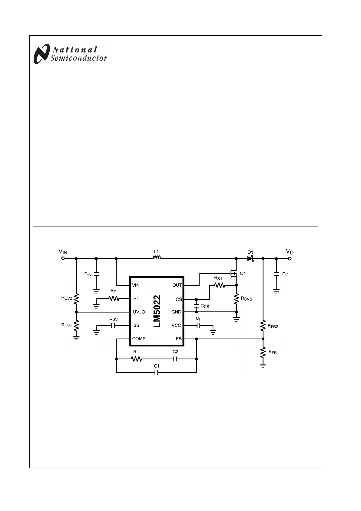
Typical Application
20212201
© 2007 National Semiconductor Corporation 202122 www.national.com
LM5022 60V Low Side Controller for Boost and SEPIC
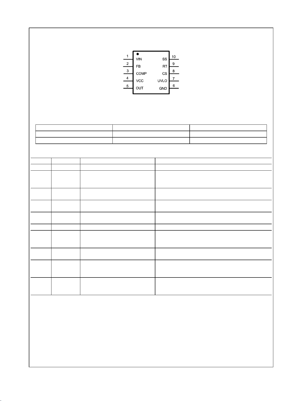
Connection Diagram
20212253
10-Lead MSOP
NS Package Number MUB10A
Ordering Information
Part Number NS Package Drawing Supplied As
LM5022MM MUB10A 1000 Units on Tape and Reel
LM5022MMX MUB10A 3500 Units on Tape and Reel
Pin Descriptions
Pin(s) Name Description Application Information
1 VIN Source input voltage Input to the start-up regulator. Operates from 6V to 60V.
2 FB Feedback pin
Inverting input to the internal voltage error amplifier. The noninverting input of the error amplifier connects to a 1.25V
reference.
3 COMP
Error amplifier output and PWM
comparator input
The control loop compensation components connect between
this pin and the FB pin.
4 VCC
Output of the internal, high voltage linear
regulator.
This pin should be bypassed to the GND pin with a ceramic
capacitor.
5 OUT Output of MOSFET gate driver Connect this pin to the gate of the external MOSFET. The gate
driver has a 1A peak current capability.
6 GND System ground
7 UVLO Input Under-Voltage Lock-out
Set the start-up and shutdown levels by connecting this pin to the
input voltage through a resistor divider. A 20 µA current source
provides hysteresis.
8 CS
Current Sense input Input for the switch current used for current mode control and for
current limiting.
9 RT/SYNC
Oscillator frequency adjust pin and
synchronization input
An external resistor connected from this pin to GND sets the
oscillator frequency. This pin can also accept an AC-coupled
input for synchronization from an external clock.
10 SS Soft-start pin
An external capacitor placed from this pin to ground will be
charged by a 10 µA current source, creating a ramp voltage to
control the regulator start-up.
www.national.com 2
LM5022
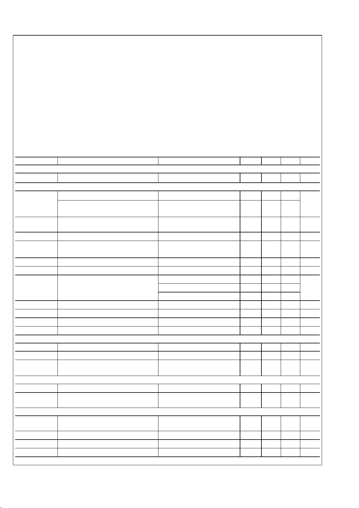
Absolute Maximum Ratings (Note 1)
If Military/Aerospace specified devices are required,
please contact the National Semiconductor Sales Office/
Distributors for availability and specifications.
VIN to GND -0.3V to 65V
VCC to GND -0.3V to 16V
RT/SYNC to GND -0.3V to 5.5V
OUT to GND -1.5V for < 100 ns
All other pins to GND -0.3V to 7V
Power Dissipation Internally Limited
Junction Temperature 150°C
Storage Temperature -65°C to +150°C
Soldering Information
Vapor Phase (60 sec.) 215°C
Infrared (15 sec.) 220°C
ESD Rating
Human Body Model (Note 2) 2 kV
Operating Ranges (Note 4)
Supply Voltage 6V to 60V
External Volatge at V
CC
7.5V to 14V
Junction Temperature Range -40°C to +125°C
Electrical Characteristics Limits in standard type are for T
J
= 25°C only; limits in boldface type apply over the
junction temperature (TJ) range of -40°C to +125°C. Minimum and Maximum limits are guaranteed through test, design, or statistical
correlation. Typical values represent the most likely parametric norm at TJ = 25°C, and are provided for reference purposes only.
VIN = 24V and RT = 27.4 kΩ unless otherwise indicated. (Note 3)
Symbol Parameter Conditions Min Typ Max Units
SYSTEM PARAMETERS
V
FB
FB Pin Voltage
-40°C ≤ T
J
≤ 125°C
1.225 1.250 1.275 V
START-UP REGULATOR
VCC
VCC Regulation
9V ≤ VIN ≤ 60V, ICC = 1 mA
6.6 7 7.4
V
VCC Regulation
6V ≤ VIN < 9V, VCC Pin Open
Circuit
5
I
CC
Supply Current
OUT Pin Capacitance = 0
VCC = 10V
3.5 4
mA
I
CC-LIM
VCC Current Limit VCC = 0V, (Note 4, 6) 15 35 mA
VIN - VCC
Dropout Voltage Across Bypass Switch
ICC = 0 mA, fSW < 200 kHz
6V ≤ VIN ≤ 8.5V
200
mV
V
BYP-HI
Bypass Switch Turn-off Threshold VIN increasing 8.7 V
V
BYP-HYS
Bypass Switch Threshold Hysteresis VIN Decreasing 260 mV
Z
VCC
VCC Pin Output Impedance
0 mA ≤ ICC ≤ 5 mA
VIN = 6.0V 58
Ω
VIN = 8.0V 53
VIN = 24.0V 1.6
VCC
-HI
VCC Pin UVLO Rising Threshold 5 V
VCC
-HYS
VCC Pin UVLO Falling Hysteresis 300 mV
I
VIN
Start-up Regulator Leakage VIN = 60V 150 500 µA
I
IN-SD
Shutdown Current V
UVLO
= 0V, VCC = Open Circuit 350 450 µA
ERROR AMPLIFIER
GBW Gain Bandwidth 4 MHz
A
DC
DC Gain 75 dB
I
COMP
COMP Pin Current Sink Capability
VFB = 1.5V
V
COMP
= 1V
5 17
mA
UVLO
V
SD
Shutdown Threshold 1.22 1.25 1.28 V
I
SD-HYS
Shutdown
Hysteresis Current Source
16 20 24
µA
CURRENT LIMIT
t
LIM-DLY
Delay from ILIM to Output
CS steps from 0V to 0.6V
OUT transitions to 90% of VCC
30
ns
V
CS
Current Limit Threshold Voltage 0.45 0.5 0.55 V
t
BLK
Leading Edge Blanking Time 65 ns
R
CS
CS Pin Sink Impedance Blanking active 40 75
Ω
3 www.national.com
LM5022
Symbol Parameter Conditions Min Typ Max Units
SOFT-START
I
SS
Soft-start Current Source 7 10 13 µA
V
SS-OFF
Soft-start to COMP Offset 0.35 0.55 0.75 V
OSCILLATOR
f
SW
RT to GND = 84.5 kΩ
(Note 5) 170 200 230 kHz
RT to GND = 27.4 kΩ
(Note 5) 525 600 675 kHz
RT to GND = 16.2 kΩ
(Note 5) 865 990 1115 kHz
V
SYNC-HI
Synchronization Rising Threshold 3.8 V
PWM COMPARATOR
t
COMP-DLY
Delay from COMP to OUT Transition
V
COMP
= 2V
CS stepped from 0V to 0.4V
25
ns
D
MIN
Minimum Duty Cycle V
COMP
= 0V 0 %
D
MAX
Maximum Duty Cycle 90 95 %
A
PWM
COMP to PWM Comparator Gain 0.33 V/V
V
COMP-OC
COMP Pin Open Circuit Voltage VFB = 0V 4.3 5.2 6.1 V
I
COMP-SC
COMP Pin Short Circuit Current V
COMP
= 0V, VFB = 1.5V 0.6 1.1 1.5 mA
SLOPE COMPENSATION
V
SLOPE
Slope Compensation Amplitude 80 105 130 mV
MOSFET DRIVER
V
SAT-HI
Output High Saturation Voltage (VCC –
VOUT)
I
OUT
= 50 mA 0.25 0.75 V
V
SAT-LO
Output Low Saturation Voltage (VOUT) I
OUT
= 100 mA 0.25 0.75 V
t
RISE
OUT Pin Rise Time OUT Pin load = 1 nF 18 ns
t
FALL
OUT Pin Fall Time OUT Pin load = 1 nF 15 ns
THERMAL CHARACTERISTICS
T
SD
Thermal Shutdown Threshold 165 °C
T
SD-HYS
Thermal Shutdown Hysteresis 25 °C
θ
JA
Junction to Ambient Thermal Resistance MUB-10A Package 200 °C/W
Note 1: Absolute Maximum Ratings are limits beyond which damage to the device may occur. The Recommended Operating Limits define the conditions within
which the device is intended to be functional. For guaranteed specifications and test conditions, see the Electrical Characteristics.
Note 2: The human body model is a 100 pF capacitor discharged through a 1.5kΩ resistor into each pin.
Note 3: Min and Max limits are 100% production tested at 25°C. Limits over the operating temperature range are guaranteed through correlation using Statistical
Quality Control (SQC) methods. Limits are used to calculate National’s Average Outgoing Quality Level (AOQL).
Note 4: Device thermal limitations may limit usable range.
Note 5: Specification applies to the oscillator frequency.
Note 6: VCC provides bias for the internal gate drive and control circuits.
www.national.com 4
LM5022
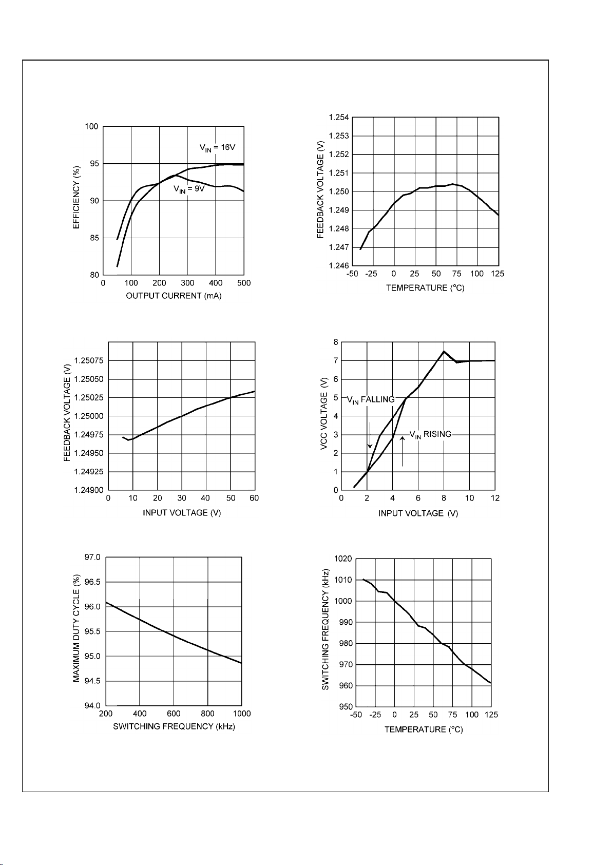
Typical Performance Characteristics
Efficiency, VO = 40V
Example Circuit BOM
20212255
VFB vs. Temp (VIN = 24V)
20212203
VFB vs. VIN (TA = 25°C)
20212204
VCC vs. VIN (TA = 25°C)
20212205
Max Duty Cycle vs. fSW (TA = 25°C)
20212206
fSW vs. Temperature (RT = 16.2 kΩ)
20212207
5 www.national.com
LM5022
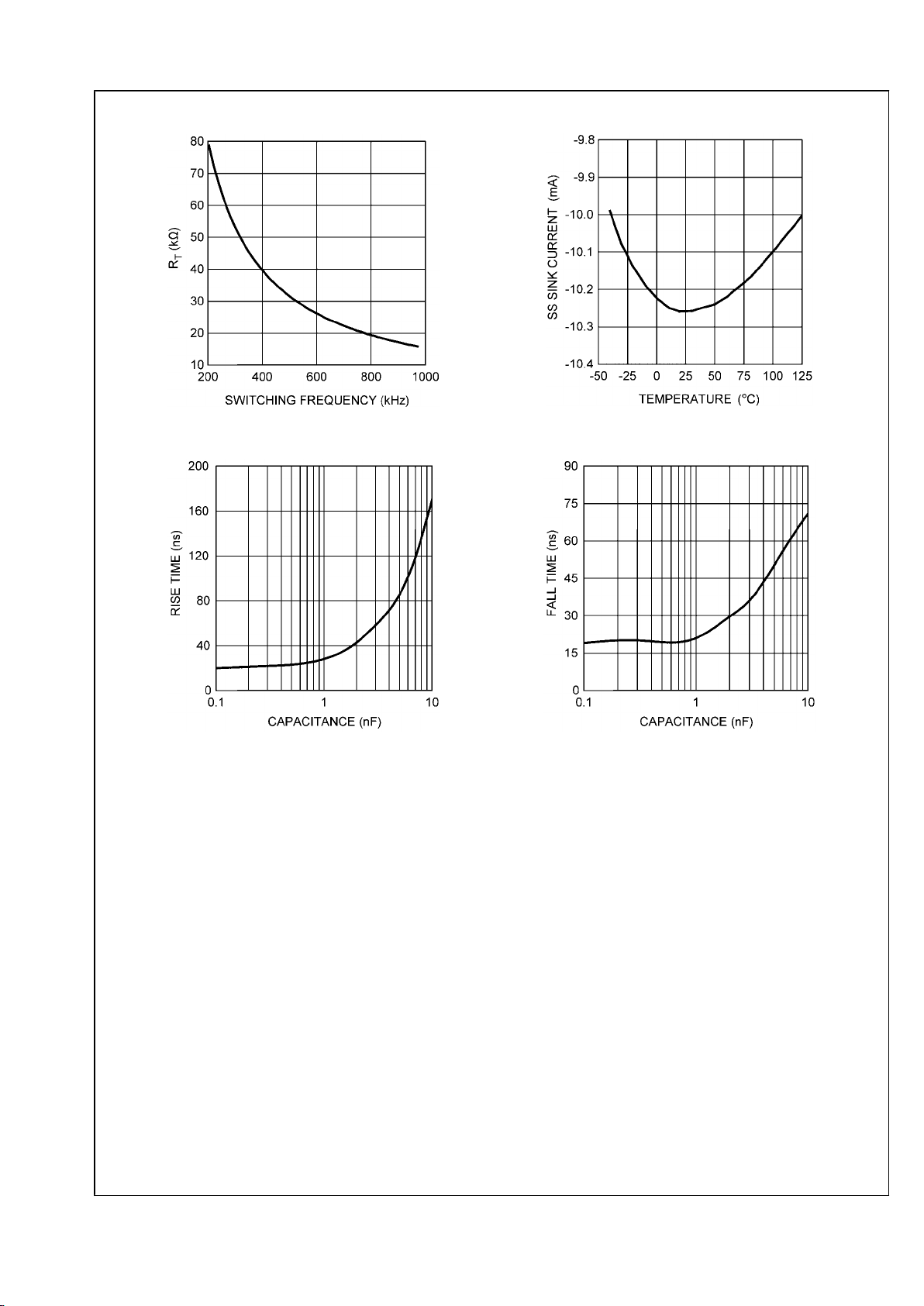
RT vs. fSW (TA = 25°C)
20212208
SS vs. Temperature
20212209
OUT Pin t
RISE
vs. Gate Capacitance
20212210
OUT Pin t
FALL
vs. Gate Capacitance
20212211
www.national.com 6
LM5022
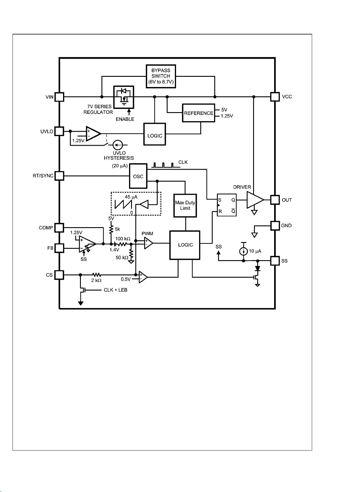
Block Diagram
20212212
7 www.national.com
LM5022

Example Circuit
20212213
FIGURE 1. Design Example Schematic
Applications Information
OVERVIEW
The LM5022 is a low-side N-channel MOSFET controller that
contains all of the features needed to implement single ended
power converter topologies. The LM5022 includes a highvoltage startup regulator that operates over a wide input
range of 6V to 60V. The PWM controller is designed for high
speed capability including an oscillator frequency range up to
2 MHz and total propagation delays less than 100 ns. Additional features include an error amplifier, precision reference,
input under-voltage lockout, cycle-by-cycle current limit, slope
compensation, soft-start, oscillator sync capability and thermal shutdown.
The LM5022 is designed for current-mode control power converters that require a single drive output, such as boost and
SEPIC topologies. The LM5022 provides all of the advantages of current-mode control including input voltage feedforward, cycle-by-cycle current limiting and simplified loop
compensation.
HIGH VOLTAGE START-UP REGULATOR
The LM5022 contains an internal high-voltage startup regulator that allows the VIN pin to be connected directly to line
voltages as high as 60V. The regulator output is internally
current limited to 35 mA (typical). When power is applied, the
regulator is enabled and sources current into an external capacitor, CF, connected to the VCC pin. The recommended
capacitance range for CF is 0.1 µF to 100 µF. When the voltage on the VCC pin reaches the rising threshold of 5V, the
controller output is enabled. The controller will remain enabled until VCC falls below 4.7V. In applications using a
transformer, an auxiliary winding can be connected through
a diode to the VCC pin. This winding should raise the VCC
pin voltage to above 7.5V to shut off the internal startup regulator. Powering VCC from an auxiliary winding improves
conversion efficiency while reducing the power dissipated in
the controller. The capacitance of CF must be high enough
that it maintains the VCC voltage greater than the VCC UVLO
falling threshold (4.7V) during the initial start-up. During a fault
condition when the converter auxiliary winding is inactive, external current draw on the VCC line should be limited such
that the power dissipated in the start-up regulator does not
exceed the maximum power dissipation capability of the controller.
An external start-up or other bias rail can be used instead of
the internal start-up regulator by connecting the VCC and the
VIN pins together and feeding the external bias voltage (7.5V
to 14V) to the two pins.
INPUT UNDER-VOLTAGE DETECTOR
The LM5022 contains an input Under Voltage Lock Out (UVLO) circuit. UVLO is programmed by connecting the UVLO
pin to the center point of an external voltage divider from VIN
to GND. The resistor divider must be designed such that the
voltage at the UVLO pin is greater than 1.25V when VIN is in
the desired operating range. If the under voltage threshold is
not met, all functions of the controller are disabled and the
controller remains in a low power standby state. UVLO hysteresis is accomplished with an internal 20 µA current source
that is switched on or off into the impedance of the set-point
divider. When the UVLO threshold is exceeded, the current
source is activated to instantly raise the voltage at the UVLO
pin. When the UVLO pin voltage falls below the 1.25V threshold the current source is turned off, causing the voltage at the
UVLO pin to fall. The UVLO pin can also be used to implement
a remote enable / disable function. If an external transistor
pulls the UVLO pin below the 1.25V threshold, the converter
will be disabled. This external shutdown method is shown in
Figure 2.
www.national.com 8
LM5022

20212214
FIGURE 2. Enable/Disable Using UVLO
ERROR AMPLIFIER
An internal high gain error amplifier is provided within the
LM5022. The amplifier’s non-inverting input is internally set to
a fixed reference voltage of 1.25V. The inverting input is connected to the FB pin. In non-isolated applications such as the
boost converter the output voltage, VO, is connected to the FB
pin through a resistor divider. The control loop compensation
components are connected between the COMP and FB pins.
For most isolated applications the error amplifier function is
implemented on the secondary side of the converter and the
internal error amplifier is not used. The internal error amplifier
is configured as an open drain output and can be disabled by
connecting the FB pin to ground. An internal 5 kΩ pull-up resistor between a 5V reference and COMP can be used as the
pull-up for an opto-coupler in isolated applications.
CURRENT SENSING AND CURRENT LIMITING
The LM5022 provides a cycle-by-cycle over current protection function. Current limit is accomplished by an internal
current sense comparator. If the voltage at the current sense
comparator input exceeds 0.5V, the MOSFET gate drive will
be immediately terminated. A small RC filter, located near the
controller, is recommended to filter noise from the current
sense signal. The CS input has an internal MOSFET which
discharges the CS pin capacitance at the conclusion of every
cycle. The discharge device remains on an additional 65 ns
after the beginning of the new cycle to attenuate leading edge
ringing on the current sense signal.
The LM5022 current sense and PWM comparators are very
fast, and may respond to short duration noise pulses. Layout
considerations are critical for the current sense filter and
sense resistor. The capacitor associated with the CS filter
must be located very close to the device and connected directly to the pins of the controller (CS and GND). If a current
sense transformer is used, both leads of the transformer secondary should be routed to the sense resistor and the current
sense filter network. The current sense resistor can be located between the source of the primary power MOSFET and
power ground, but it must be a low inductance type. When
designing with a current sense resistor all of the noise sensitive low-power ground connections should be connected together locally to the controller and a single connection should
be made to the high current power ground (sense resistor
ground point).
OSCILLATOR, SHUTDOWN AND SYNC
A single external resistor, RT, connected between the RT/
SYNC and GND pins sets the LM5022 oscillator frequency.
To set the switching frequency, fSW, RT can be calculated
from:
The LM5022 can also be synchronized to an external clock.
The external clock must have a higher frequency than the free
running oscillator frequency set by the RT resistor. The clock
signal should be capacitively coupled into the RT/SYNC pin
with a 100 pF capacitor as shown in Figure 3. A peak voltage
level greater than 3.8V at the RT/SYNC pin is required for
detection of the sync pulse. The sync pulse width should be
set between 15 ns to 150 ns by the external components. The
RT resistor is always required, whether the oscillator is free
running or externally synchronized. The voltage at the RT/
SYNC pin is internally regulated to 2V, and the typical delay
from a logic high at the RT/SYNC pin to the rise of the OUT
pin voltage is 120 ns. RT should be located very close to the
device and connected directly to the pins of the controller (RT/
SYNC and GND).
20212254
FIGURE 3. Sync Operation
PWM COMPARATOR AND SLOPE COMPENSATION
The PWM comparator compares the current ramp signal with
the error voltage derived from the error amplifier output. The
error amplifier output voltage at the COMP pin is offset by
1.4V and then further attenuated by a 3:1 resistor divider. The
PWM comparator polarity is such that 0V on the COMP pin
will result in a zero duty cycle at the controller output. For duty
cycles greater than 50%, current mode control circuits can
experience sub-harmonic oscillation. By adding an additional
fixed-slope voltage ramp signal (slope compensation) this oscillation can be avoided. Proper slope compensation damps
the double pole associated with current mode control (see the
Control Loop Compensation section) and eases the design of
the control loop compensator. The LM5022 generates the
slope compensation with a sawtooth-waveform current
source with a slope of 45 µA x fSW, generated by the clock.
(See Figure 4) This current flows through an internal 2 kΩ
9 www.national.com
LM5022

resistor to create a minimum compensation ramp with a slope
of 100 mV x fSW (typical). The slope of the compensation ramp
increases when external resistance is added for filtering the
current sense (RS1) or in the position RS2. As shown in Figure
4 and the block diagram, the sensed current slope and the
compensation slope add together to create the signal used
for current limiting and for the control loop itself.
20212216
FIGURE 4. Slope Compensation
In peak current mode control the optimal slope compensation
is proportional to the slope of the inductor current during the
power switch off-time. For boost converters the inductor current slope while the MOSFET is off is (VO - VIN) / L. This
relationship is combined with the requirements to set the peak
current limit and is used to select R
SNS
and RS2 in the Design
Considerations section.
SOFT-START
The soft-start feature allows the power converter output to
gradually reach the initial steady state output voltage, thereby
reducing start-up stresses and current surges. At power on,
after the VCC and input under-voltage lockout thresholds are
satisfied, an internal 10 µA current source charges an external
capacitor connected to the SS pin. The capacitor voltage will
ramp up slowly and will limit the COMP pin voltage and the
switch current.
MOSFET GATE DRIVER
The LM5022 provides an internal gate driver through the OUT
pin that can source and sink a peak current of 1A to control
external, ground-referenced N-channel MOSFETs.
THERMAL SHUTDOWN
Internal thermal shutdown circuitry is provided to protect the
LM5022 in the event that the maximum junction temperature
is exceeded. When activated, typically at 165°C, the controller
is forced into a low power standby state, disabling the output
driver and the VCC regulator. After the temperature is reduced (typical hysteresis is 25°C) the VCC regulator will be
re-enabled and the LM5022 will perform a soft-start.
Design Considerations
The most common circuit controlled by the LM5022 is a nonisolated boost regulator. The boost regulator steps up the
input voltage and has a duty ratio D of:
(VD is the forward voltage drop of the output diode)
The following is a design procedure for selecting all the components for the boost converter circuit shown in Figure 1. The
application is "in-cabin" automotive, meaning that the operating ambient temperature ranges from -20°C to 85°C. This
circuit operates in continuous conduction mode (CCM),
where inductor current stays above 0A at all times, and delivers an output voltage of 40.0V ±2% at a maximum output
current of 0.5A. Additionally, the regulator must be able to
handle a load transient of up to 0.5A while keeping VO within
±4%. The voltage input comes from the battery/alternator
system of an automobile, where the standard range 9V to 16V
and transients of up to 32V must not cause any malfunction.
SWITCHING FREQUENCY
The selection of switching frequency is based on the tradeoffs
between size, cost, and efficiency. In general, a lower frequency means larger, more expensive inductors and capacitors will be needed. A higher switching frequency generally
results in a smaller but less efficient solution, as the power
MOSFET gate capacitances must be charged and discharged more often in a given amount of time. For this application, a frequency of 500 kHz was selected as a good
compromise between the size of the inductor and efficiency.
PCB area and component height are restricted in this application. Following the equation given for RT in the Applications
Information section, a 33.2 kΩ 1% resistor should be used to
switch at 500 kHz.
MOSFET
Selection of the power MOSFET is governed by tradeoffs between cost, size, and efficiency. Breaking down the losses in
the MOSFET is one way to determine relative efficiencies between different devices. For this example, the SO-8 package
provides a balance of a small footprint with good efficiency.
Losses in the MOSFET can be broken down into conduction
loss, gate charging loss, and switching loss.
Conduction, or I2R loss, PC, is approximately:
www.national.com 10
LM5022

The factor 1.3 accounts for the increase in MOSFET on resistance due to heating. Alternatively, the factor of 1.3 can be
ignored and the maximum on resistance of the MOSFET can
be used.
Gate charging loss, PG, results from the current required to
charge and discharge the gate capacitance of the power
MOSFET and is approximated as:
PG = VCC x QG x f
SW
QG is the total gate charge of the MOSFET. Gate charge loss
differs from conduction and switching losses because the actual dissipation occurs in the LM5022 and not in the MOSFET
itself. If no external bias is applied to the VCC pin, additional
loss in the LM5022 IC occurs as the MOSFET driving current
flows through the VCC regulator. This loss, P
VCC
, is estimated
as:
P
VCC
= (VIN – VCC) x QG x f
SW
Switching loss, PSW, occurs during the brief transition period
as the MOSFET turns on and off. During the transition period
both current and voltage are present in the channel of the
MOSFET. The loss can be approximated as:
PSW = 0.5 x VIN x [IO / (1 – D)] x (tR + tF) x f
SW
Where tR and tF are the rise and fall times of the MOSFET
For this example, the maximum drain-to-source voltage applied across the MOSFET is VO plus the ringing due to parasitic inductance and capacitance. The maximum drive voltage
at the gate of the high side MOSFET is VCC, or 7V typical.
The MOSFET selected must be able to withstand 40V plus
any ringing from drain to source, and be able to handle at least
7V plus ringing from gate to source. A minimum voltage rating
of 50V
D-S
and 10V
G-S
MOSFET will be used. Comparing the
losses in a spreadsheet leads to a 60V
D-S
rated MOSFET in
SO-8 with an R
DSON
of 22 mΩ (the maximum vallue is 31
mΩ), a gate charge of 27 nC, and rise and falls times of 10 ns
and 12 ns, respectively.
OUTPUT DIODE
The boost regulator requires an output diode D1 (see Figure
1) to carrying the inductor current during the MOSFET off-
time. The most efficient choice for D1 is a Schottky diode due
to low forward drop and near-zero reverse recovery time. D1
must be rated to handle the maximum output voltage plus any
switching node ringing when the MOSFET is on. In practice,
all switching converters have some ringing at the switching
node due to the diode parasitic capacitance and the lead inductance. D1 must also be rated to handle the average output
current, IO.
The overall converter efficiency becomes more dependent on
the selection of D1 at low duty cycles, where the boost diode
carries the load current for an increasing percentage of the
time. This power dissipation can be calculating by checking
the typical diode forward voltage, VD, from the I-V curve on
the diode's datasheet and then multiplying it by IO. Diode
datasheets will also provide a typical junction-to-ambient thermal resistance, θJA, which can be used to estimate the operating die temperature of the Schottky. Multiplying the power
dissipation (PD = IO x VD) by θJA gives the temperature rise.
The diode case size can then be selected to maintain the
Schottky diode temperature below the operational maximum.
In this example a Schottky diode rated to 60V and 1A will be
suitable, as the maximum diode current will be 0.5A. A small
case such as SOD-123 can be used if a small footprint is critical. Larger case sizes generally have lower θJA and lower
forward voltage drop, so for better efficiency the larger SMA
case size will be used.
BOOST INDUCTOR
The first criterion for selecting an inductor is the inductance
itself. In fixed-frequency boost converters this value is based
on the desired peak-to-peak ripple current, ΔiL, which flows in
the inductor along with the average inductor current, IL. For a
boost converter in CCM IL is greater than the average output
current, IO. The two currents are related by the following expression:
IL = IO / (1 – D)
As with switching frequency, the inductance used is a tradeoff
between size and cost. Larger inductance means lower input
ripple current, however because the inductor is connected to
the output during the off-time only there is a limit to the reduction in output ripple voltage. Lower inductance results in
smaller, less expensive magnetics. An inductance that gives
a ripple current of 30% to 50% of IL is a good starting point for
a CCM boost converter. Minimum inductance should be calculated at the extremes of input voltage to find the operating
condition with the highest requirement:
By calculating in terms of amperes, volts, and megahertz, the
inductance value will come out in micro henries.
In order to ensure that the boost regulator operates in CCM
a second equation is needed, and must also be evaluated at
the corners of input voltage to find the minimum inductance
required:
By calculating in terms of volts, amps and megahertz the inductance value will come out in µH.
For this design ΔiL will be set to 40% of the maximum IL. Duty
cycle is evaluated first at V
IN(MIN)
and at V
IN(MAX)
. Second, the
average inductor current is evaluated at the two input voltages. Third, the inductor ripple current is determined. Finally,
the inductance can be calculated, and a standard inductor
value selected that meets all the criteria.
Inductance for Minimum Input Voltage
D
VIN(MIN)
= (40 – 9.0 + 0.5) / (40 + 0.5) = 78%
I
L-VIN(MIN)
= 0.5 / (1 – 0.78) = 2.3A
ΔiL = 0.4 x 2.3A = 0.92A
11 www.national.com
LM5022

Inductance for Maximum Input Voltage
D
VIN(MAX)
= (40 - 16 + 0.5) / (40 + 0.5) = 60%
I
L-VIN(MIAX)
= 0.5 / (1 – 0.6) = 1.25A
ΔiL = 0.4 x 1.25A = 0.5A
Maximum average inductor current occurs at V
IN(MIN)
, and the
corresponding inductor ripple current is 0.92A
P-P
. Selecting
an inductance that exceeds the ripple current requirement at
V
IN(MIN)
and the requirement to stay in CCM for V
IN(MAX)
provides a tradeoff that allows smaller magnetics at the cost of
higher ripple current at maximum input voltage. For this example, a 33 µH inductor will satisfy these requirements.
The second criterion for selecting an inductor is the peak current carrying capability. This is the level above which the
inductor will saturate. In saturation the inductance can drop
off severely, resulting in higher peak current that may overheat the inductor or push the converter into current limit. In a
boost converter, peak current, IPK, is equal to the maximum
average inductor current plus one half of the ripple current.
First, the current ripple must be determined under the conditions that give maximum average inductor current:
Maximum average inductor current occurs at V
IN(MIN)
. Using
the selected inductance of 33 µH yields the following:
ΔiL = (9 x 0.78) / (0.5 x 33) = 425 mA
P-P
The highest peak inductor current over all operating conditions is therefore:
IPK = IL + 0.5 x ΔiL = 2.3 + 0.213 = 2.51A
Hence an inductor must be selected that has a peak current
rating greater than 2.5A and an average current rating greater
than 2.3A. One possibility is an off-the-shelf 33 µH ±20% inductor that can handle a peak current of 3.2A and an average
current of 3.4A. Finally, the inductor current ripple is recalculated at the maximum input voltage:
Δi
L-VIN(MAX)
= (16 x 0.6) / (0.5 x 33) = 0.58A
P-P
OUTPUT CAPACITOR
The output capacitor in a boost regulator supplies current to
the load during the MOSFET on-time and also filters the AC
portion of the load current during the off-time. This capacitor
determines the steady state output voltage ripple, ΔVO, a critical parameter for all voltage regulators. Output capacitors are
selected based on their capacitance, CO, their equivalent series resistance (ESR) and their RMS or AC current rating.
The magnitude of ΔVO is comprised of three parts, and in
steady state the ripple voltage during the on-time is equal to
the ripple voltage during the off-time. For simplicity the analysis will be performed for the MOSFET turning off (off-time)
only. The first part of the ripple voltage is the surge created
as the output diode D1 turns on. At this point inductor/diode
current is at the peak value, and the ripple voltage increase
can be calculated as:
ΔVO1 = IPK x ESR
The second portion of the ripple voltage is the increase due
to the charging of CO through the output diode. This portion
can be approximated as:
ΔVO2 = (IO / CO) x (D / fSW)
The final portion of the ripple voltage is a decrease due to the
flow of the diode/inductor current through the output
capacitor’s ESR. This decrease can be calculated as:
ΔVO3 = ΔiL x ESR
The total change in output voltage is then:
ΔVO = ΔVO1 + ΔVO2 - ΔV
O3
The combination of two positive terms and one negative term
may yield an output voltage ripple with a net rise or a net fall
during the converter off-time. The ESR of the output capacitor
(s) has a strong influence on the slope and direction of ΔVO.
Capacitors with high ESR such as tantalum and aluminum
electrolytic create an output voltage ripple that is dominated
by ΔVO1 and ΔVO3, with a shape shown in Figure 5. Ceramic
capacitors, in contrast, have very low ESR and lower capacitance. The shape of the output ripple voltage is dominated by
ΔVO2, with a shape shown in Figure 6.
20212226
FIGURE 5. ΔVO Using High ESR Capacitors
www.national.com 12
LM5022

20212227
FIGURE 6. ΔVO Using Low ESR Capacitors
For this example the small size and high temperature rating
of ceramic capacitors make them a good choice. The output
ripple voltage waveform of Figure 6 is assumed, and the capacitance will be selected first. The desired ΔVO is ±2% of
40V, or 0.8V
P-P
. Beginning with the calculation for ΔVO2, the
required minimum capacitance is:
C
O-MIN
= (IO / ΔVO) x (D
MAX
/ fSW)
C
O-MIN
= (0.5 / 0.8) x (0.77 / 5 x 10⁵) = 0.96 µF
The next higher standard 20% capacitor value is 1.0 µF, however to provide margin for component tolerance and load
transients two capacitors rated 4.7 µF each will be used. Ceramic capacitors rated 4.7 µF ±20% are available from many
manufacturers. The minimum quality dielectric that is suitable
for switching power supply output capacitors is X5R, while
X7R (or better) is preferred. Careful attention must be paid to
the DC voltage rating and case size, as ceramic capacitors
can lose 60% or more of their rated capacitance at the maximum DC voltage. This is the reason that ceramic capacitors
are often de-rated to 50% of their capacitance at their working
voltage. The output capacitors for this example will have a
100V rating in a 2220 case size.
The typical ESR of the selected capacitors is 3 mΩ each, and
in parallel is approximately 1.5 mΩ. The worst-case value for
ΔVO1 occurs during the peak current at minimum input volt-
age:
ΔVO1 = 2.5 x 0.0015 = 4 mV
The worst-case capacitor charging ripple occurs at maximum
duty cycle:
ΔVO2 = (0.5 / 9.4 x 10-6) x (0.77 / 5 x 10⁵) = 82 mV
Finally, the worst-case value for ΔVO3 occurs when inductor
ripple current is highest, at maximum input voltage:
ΔVO3 = 0.58 x 0.0015 = 1 mV (negligible)
The output voltage ripple can be estimated by summing the
three terms:
ΔVO = 4 mV + 82 mV - 1 mV = 85 mV
The RMS current through the output capacitor(s) can be estimated using the following, worst-case equation:
The highest RMS current occurs at minimum input voltage.
For this example the maximum output capacitor RMS current
is:
I
O-RMS(MAX)
= 1.13 x 2.3 x (0.78 x 0.22)
0.5
= 1.08A
RMS
These 2220 case size devices are capable of sustaining RMS
currents of over 3A each, making them more than adequate
for this application.
VCC DECOUPLING CAPACITOR
The VCC pin should be decoupled with a ceramic capacitor
placed as close as possible to the VCC and GND pins of the
LM5022. The decoupling capacitor should have a minimum
X5R or X7R type dielectric to ensure that the capacitance remains stable over voltage and temperature, and be rated to
a minimum of 470 nF. One good choice is a 1.0 µF device
with X7R dielectric and 1206 case size rated to 25V.
INPUT CAPACITOR
The input capacitors to a boost regulator control the input
voltage ripple, ΔVIN, hold up the input voltage during load
transients, and prevent impedance mismatch (also called
power supply interaction) between the LM5022 and the inductance of the input leads. Selection of input capacitors is
based on their capacitance, ESR, and RMS current rating.
The minimum value of ESR can be selected based on the
maximum output current transient, I
STEP
, using the following
expression:
For this example the maximum load step is equal to the load
current, or 0.5A. The maximum permissable ΔVIN during load
transients is 4%
P-P
. ΔVIN and duty cycle are taken at minimum
input voltage to give the worst-case value:
ESR
MIN
= [(1 – 0.77) x 0.36] / (2 x 0.5) = 83 mΩ
The minimum input capacitance can be selected based on
ΔVIN, based on the drop in VIN during a load transient, or
based on prevention of power supply interaction. In general,
the requirement for greatest capacitance comes from the
power supply interaction. The inductance and resistance of
the input source must be estimated, and if this information is
not available, they can be assumed to be 1 µH and 0.1Ω, re-
spectively. Minimum capacitance is then estimated as:
As with ESR, the worst-case, highest minimum capacitance
calculation comes at the minimum input voltage. Using the
default estimates for LS and RS, minimum capacitance is:
13 www.national.com
LM5022

The next highest standard 20% capacitor value is 6.8 µF, but
because the actual input source impedance and resistance
are not known, two 4.7 µF capacitors will be used. In general,
doubling the calculated value of input capacitance provides a
good safety margin. The final calculation is for the RMS current. For boost converters operating in CCM this can be
estimated as:
I
RMS
= 0.29 x Δi
L(MAX)
From the inductor section, maximum inductor ripple current is
0.58A, hence the input capacitor(s) must be rated to handle
0.29 x 0.58 = 170 mA
RMS
.
The input capacitors can be ceramic, tantalum, aluminum, or
almost any type, however the low capacitance requirement
makes ceramic capacitors particularly attractive. As with the
output capacitors, the minimum quality dielectric used should
X5R, with X7R or better preferred. The voltage rating for input
capacitors need not be as conservative as the output capacitors, as the need for capacitance decreases as input voltage
increases. For this example, the capacitor selected will be 4.7
µF ±20%, rated to 50V, in the 1812 case size. The RMS current rating of these capacitors is over 2A each, more than
enough for this application.
CURRENT SENSE FILTER
Parasitic circuit capacitance, inductance and gate drive current create a spike in the current sense voltage at the point
where Q1 turns on. In order to prevent this spike from terminating the on-time prematurely, every circuit should have a
low-pass filter that consists of CCS and RS1, shown in Figure
1. The time constant of this filter should be long enough to
reduce the parasitic spike without significantly affecting the
shape of the actual current sense voltage. The recommended
range for RS1 is between 10Ω and 500Ω, and the recommended range for CCS is between 100 pF and 2.2 nF. For this
example, the values of RS1 and CCS will be 100Ω and 1 nF,
respectively.
R
SNS
, RS2 AND CURRENT LIMIT
The current sensing resistor R
SNS
is used for steady state
regulation of the inductor current and to sense over-current
conditions. The slope compensation resistor is used to ensure
control loop stability, and both resistors affect the current limit
threshold. The R
SNS
value selected must be low enough to
keep the power dissipation to a minimum, yet high enough to
provide good signal-to-noise ratio for the current sensing circuitry. R
SNS
, and RS2 should be set so that the current limit
comparator, with a threshold of 0.5V, trips before the sensed
current exceeds the peak current rating of the inductor, without limiting the output power in steady state.
For this example the peak current, at V
IN(MIN)
, is 2.5A, while
the inductor itself is rated to 3.2A. The threshold for current
limit, I
LIM
, is set slightly between these two values to account
for tolerance of the circuit components, at a level of 3.0A. The
required resistor calculation must take into account both the
switch current through R
SNS
and the compensation ramp cur-
rent flowing through the internal 2 kΩ, RS1 and RS2 resistors.
R
SNS
should be selected first because it is a power resistor
with more limited selection. The following equation should be
evaluated at V
IN(MIN)
, when duty cycle is highest:
L in µH, fSW in MHz
The closest 5% value is 100 mΩ. Power dissipation in R
SNS
can be estimated by calculating the average current. The
worst-case average current through R
SNS
occurs at minimum
input voltage/maximum duty cycle and can be calculated as:
PCS = [(0.5 / 0.22)2 x 0.1] x 0.78 = 0.4W
For this example a 0.1Ω ±1%, thick-film chip resistor in a 1210
case size rated to 0.5W will be used.
With R
SNS
selected, RS2 can be determined using the follow-
ing expression:
The closest 1% tolerance value is 3.57 kΩ.
CONTROL LOOP COMPENSATION
The LM5022 uses peak current-mode PWM control to correct
changes in output voltage due to line and load transients.
Peak current-mode provides inherent cycle-by-cycle current
limiting, improved line transient response, and easier control
loop compensation.
The control loop is comprised of two parts. The first is the
power stage, which consists of the pulse width modulator,
output filter, and the load. The second part is the error amplifier, which is an op-amp configured as an inverting amplifier.
Figure 7 shows the regulator control loop components.
www.national.com 14
LM5022

20212234
FIGURE 7. Power Stage and Error Amp
One popular method for selecting the compensation components is to create Bode plots of gain and phase for the power
stage and error amplifier. Combined, they make the overall
bandwidth and phase margin of the regulator easy to determine. Software tools such as Excel, MathCAD, and Matlab
are useful for observing how changes in compensation or the
power stage affect system gain and phase.
The power stage in a CCM peak current mode boost converter consists of the DC gain, APS, a single low frequency
pole, f
LFP
, the ESR zero, f
ZESR
, a right-half plane zero, f
RHP
,
and a double pole resulting from the sampling of the peak
current. The power stage transfer function (also called the
Control-to-Output transfer function) can be written:
Where the DC gain is defined as:
Where:
RO = VO / I
O
The system ESR zero is:
The low frequency pole is:
The right-half plane zero is:
The sampling double pole quality factor is:
The sampling double corner frequency is:
ωn = π x f
SW
The natural inductor current slope is:
Sn = R
SNS
x VIN / L
The external ramp slope is:
Se = 45 µA x (2000 + RS1 + RS2)] x f
SW
In the equation for APS, DC gain is highest when input voltage
and output current are at the maximum. In this the example
those conditions are VIN = 16V and IO = 500 mA.
DC gain is 44 dB. The low frequency pole fP = 2πωP is at
423Hz, the ESR zero fZ = 2πωZ is at 5.6 MHz, and the righthalf plane zero f
RHP
= 2πω
RHP
is at 61 kHz. The sampling
double-pole occurs at one-half of the switching frequency.
Proper selection of slope compensation (via RS2) is most evident the sampling double pole. A well-selected RS2 value
eliminates peaking in the gain and reduces the rate of change
of the phase lag. Gain and phase plots for the power stage
are shown in Figure 8.
20212241
15 www.national.com
LM5022

20212297
FIGURE 8. Power Stage Gain and Phase
The single pole causes a roll-off in the gain of -20 dB/decade
at lower frequency. The combination of the RHP zero and
sampling double pole maintain the slope out to beyond the
switching frequency. The phase tends towards -90° at lower
frequency but then increases to -180° and beyond from the
RHP zero and the sampling double pole. The effect of the
ESR zero is not seen because its frequency is several
decades above the switching frequency. The combination of
increasing gain and decreasing phase makes converters with
RHP zeroes difficult to compensate. Setting the overall control loop bandwidth to 1/3 to 1/10 of the RHP zero frequency
minimizes these negative effects, but requires a compromise
in the control loop bandwidth. If this loop were left uncompensated, the bandwidth would be 89 kHz and the phase
margin -54°. The converter would oscillate, and therefore is
compensated using the error amplifier and a few passive
components.
The transfer function of the compensation block, GEA, can be
derived by treating the error amplifier as an inverting op-amp
with input impedance ZI and feedback impedance ZF. The
majority of applications will require a Type II, or two-pole onezero amplifier, shown in Figure 7. The LaPlace domain transfer function for this Type II network is given by the following:
Many techniques exist for selecting the compensation component values. The following method is based upon setting
the mid-band gain of the error amplifier transfer function first
and then positioning the compensation zero and pole:
1.
Determine the desired control loop bandwidth: The
control loop bandwidth, f
0dB
, is the point at which the total
control loop gain (H = GPS x GEA) is equal to 0 dB. For
this example, a low bandwidth of 10 kHz, or
approximately 1/6th of the RHP zero frequency, is
chosen because of the wide variation in input voltage.
2.
Determine the gain of the power stage at f
0dB
: This
value, A, can be read graphically from the gain plot of
GPS or calculated by replacing the ‘s’ terms in GPS with
‘2πf
0dB
’. For this example the gain at 10 kHz is
approximately 16 dB.
3.
Calculate the negative of A and convert it to a linear
gain: By setting the mid-band gain of the error amplifier
to the negative of the power stage gain at f
0dB
, the control
loop gain will equal 0 dB at that frequency. For this
example, -16 dB = 0.15V/V.
4.
Select the resistance of the top feedback divider
resistor R
FB2
: This value is arbitrary, however selecting
a resistance between 10 kΩ and 100 kΩ will lead to
practical values of R1, C1 and C2. For this example,
R
FB2
= 20 kΩ 1%.
5.
Set R1 = A x R
FB2
: For this example: R1 = 0.15 x 20000
= 3 kΩ
6.
Select a frequency for the compensation zero, fZ1:
The suggested placement for this zero is at the low
frequency pole of the power stage, f
LFP
= ωLFP / 2π. For
this example, fZ1 = f
LFP
= 423Hz
7.
Set
For this example, C2 = 125 nF
8.
Select a frequency for the compensation pole, fP1:
The suggested placement for this pole is at one-fifth of
the switching frequency. For this example, fP1 = 100 kHz
9.
Set
For this example, C1 = 530 pF
10.
Plug the closest 1% tolerance values for R
FB2
and R1,
then the closest 10% values for C1 and C2 into G
EA
and model the error amp: The open-loop gain and
bandwidth of the LM5022’s internal error amplifier are 75
dB and 4 MHz, respectively. Their effect on GEA can be
modeled using the following expression:
ADC is a linear gain, the linear equivalent of 75 dB is
approximately 5600V/V. C1 = 560 pF 10%, C2 = 120 nF
10%, R1 = 3.01 kΩ 1%
11.
Plot or evaluate the actual error amplifier transfer
function:
www.national.com 16
LM5022

20212248
20212298
FIGURE 9. Error Amplifier Gain and Phase
12. Plot or evaluate the complete control loop transfer
function: The complete control loop transfer function is ob-
tained by multiplying the power stage and error amplifier
functions together. The bandwidth and phase margin can
then be read graphically or evaluated numerically.
20212249
20212299
FIGURE 10. Overall Loop Gain and Phase
The bandwidth of this example circuit at VIN = 16V is 10.5 kHz,
with a phase margin of 66°.
13. Re-evaluate at the corners of input voltage and output
current: Boost converters exhibit significant change in their
loop response when VIN and IO change. With the compensation fixed, the total control loop gain and phase should be
checked to ensure a minimum phase margin of 45° over both
line and load.
Efficiency Calculations
A reasonable estimation for the efficiency of a boost regulator
controlled by the LM5022 can be obtained by adding together
the loss is each current carrying element and using the equation:
The following shows an efficiency calculation to complement
the circuit design from the Design Considerations section.
Output power for this circuit is 40V x 0.5A = 20W. Input voltage
is assumed to be 13.8V, and the calculations used assume
that the converter runs in CCM. Duty cycle for VIN = 13.8V is
66%, and the average inductor current is 1.5A.
CHIP OPERATING LOSS
This term accounts for the current drawn at the VIN pin. This
current, IIN, drives the logic circuitry and the power MOSFETs.
The gate driving loss term from the power MOSFET section
of Design Considerations is included in the chip operating
loss. For the LM5022, IIN is equal to the steady state operating
current, ICC, plus the MOSFET driving current, IGC. Power is
lost as this current passes through the internal linear regulator
of the LM5022.
IGC = QG X f
SW
IGC = 27 nC x 500 kHz = 13.5 mA
ICC is typically 3.5 mA, taken from the Electrical Characteristics table. Chip Operating Loss is then:
PQ = VIN X (IQ + IGC)
17 www.national.com
LM5022

PQ = 13.8 X (3.5m + 13.5m) = 235 mW
MOSFET SWITCHING LOSS
PSW = 0.5 x VIN x IL x (tR + tF) x f
SW
PSW = 0.5 x 13.8 x 1.5 x (10 ns + 12 ns) x 5 x 105 = 114 mW
MOSFET AND R
SNS
CONDUCTION LOSS
PC = D x (I
L
2
x (R
DSON
x 1.3 + R
SNS
))
PC = 0.66 x (1.52 x (0.029 + 0.1)) = 192 mW
OUTPUT DIODE LOSS
The average output diode current is equal to IO, or 0.5A. The
estimated forward drop, VD, is 0.5V. The output diode loss is
therefore:
PD1 = IO x V
D
PD1 = 0.5 x 0.5 = 0.25W
INPUT CAPACITOR LOSS
This term represents the loss as input ripple current passes
through the ESR of the input capacitor bank. In this equation
‘n’ is the number of capacitors in parallel. The 4.7 µF input
capacitors selected have a combined ESR of approximately
1.5 mΩ, and ΔiL for a 13.8V input is 0.55A:
I
IN-RMS
= 0.29 x ΔiL = 0.29 x 0.55 = 0.16A
P
CIN
= [0.162 x 0.0015] / 2 = 0.02 mW (negligible)
OUTPUT CAPACITOR LOSS
This term is calculated using the same method as the input
capacitor loss, substituting the output capacitor RMS current
for VIN = 13.8V. The output capacitors' combined ESR is also
approximately 1.5 mΩ.
I
O-RMS
= 1.13 x 1.5 x (0.66 x 0.34)
0.5
= 0.8A
PCO = [0.8 x 0.0015] / 2 = 0.6 mW
BOOST INDUCTOR LOSS
The typical DCR of the selected inductor is 40 mΩ.
P
DCR
= I
L
2
x DCR
P
DCR
= 1.52 x 0.04 = 90 mW
Core loss in the inductor is estimated to be equal to the DCR
loss, adding an additional 90 mW to the total inductor loss.
TOTAL LOSS
P
LOSS
= Sum of All Loss Terms = 972 mW
EFFICIENCY
η = 20 / (20 + 0.972) = 95%
Layout Considerations
To produce an optimal power solution with the LM5022, good
layout and design of the PCB are as important as the component selection. The following are several guidelines to aid
in creating a good layout.
FILTER CAPACITORS
The low-value ceramic filter capacitors are most effective
when the inductance of the current loops that they filter is
minimized. Place C
INX
as close as possible to the VIN and
GND pins of the LM5022. Place COX close to the load, and
CF next to the VCC and GND pins of the LM5022.
SENSE LINES
The top of R
SNS
should be connected to the CS pin with a
separate trace made as short as possible. Route this trace
away from the inductor and the switch node (where D1, Q1,
and L1 connect). For the voltage loop, keep R
FB1/2
close to
the LM5022 and run a trace from as close as possible to the
positive side of COX to R
FB2
. As with the CS line, the FB line
should be routed away from the inductor and the switch node.
These measures minimize the length of high impedance lines
and reduce noise pickup.
COMPACT LAYOUT
Parasitic inductance can be reduced by keeping the power
path components close together and keeping the area of the
loops that high currents travel small. Short, thick traces or
copper pours (shapes) are best. In particular, the switch node
should be just large enough to connect all the components
together without excessive heating from the current it carries.
The LM5022 (boost converter) operates in two distinct cycles
whose high current paths are shown in Figure 11:
20212252
FIGURE 11. Boost Converter Current Loops
www.national.com 18
LM5022

The dark grey, inner loops represents the high current paths
during the MOSFET on-time. The light grey, outer loop represents the high current path during the off-time.
GROUND PLANE AND SHAPE ROUTING
The diagram of Figure 11 is also useful for analyzing the flow
of continuous current vs. the flow of pulsating currents. The
circuit paths with current flow during both the on-time and offtime are considered to be continuous current, while those that
carry current during the on-time or off-time only are pulsating
currents. Preference in routing should be given to the pulsating current paths, as these are the portions of the circuit most
likely to emit EMI. The ground plane of a PCB is a conductor
and return path, and it is susceptible to noise injection just as
any other circuit path. The continuous current paths on the
ground net can be routed on the system ground plane with
less risk of injecting noise into other circuits. The path between the input source, input capacitor and the MOSFET and
the path between the output capacitor and the load are examples of continuous current paths. In contrast, the path
between the grounded side of the power switch and the negative output capacitor terminal carries a large pulsating current. This path should be routed with a short, thick shape,
preferably on the component side of the PCB. Multiple vias in
parallel should be used right at the negative pads of the input
and output capacitors to connect the component side shapes
to the ground plane. Vias should not be placed directly at the
grounded side of the MOSFET (or R
SNS
) as they tend to inject
noise into the ground plane. A second pulsating current loop
that is often ignored but must be kept small is the gate drive
loop formed by the OUT and VCC pins, Q1, R
SNS
and capac-
itor CF.
19 www.national.com
LM5022

BOM for Example Circuit
ID Part Number Type Size Parameters Qty Vendor
U1 LM5022 Low-Side Controller MSOP-10 60V 1 NSC
Q1 Si4850EY MOSFET SO-8
60V, 31mΩ, 27nC
1 Vishay
D1 CMSH2-60M Schottky Diode SMA 60V, 2A 1 Central Semi
L1 SLF12575T-M3R2 Inductor 12.5 x 12.5 x 7.5 mm
33µH, 3.2A, 40mΩ
1 TDK
Cin1, Cin2 C4532X7R1H475M Capacitor 1812
4.7µF, 50V, 3mΩ
2 TDK
Co1, Co2 C5750X7R2A475M Capacitor 2220
4.7µF,100V, 3mΩ
2 TDK
Cf C2012X7R1E105K Capacitor 0805 1µF, 25V 1 TDK
Cinx
Cox
C2012X7R2A104M Capacitor 0805 100nF, 100V 2 TDK
C1 VJ0805A561KXXAT Capacitor 0805 560pF 10% 1 Vishay
C2 VJ0805Y124KXXAT Capacitor 0805 120nF 10% 1 Vishay
Css VJ0805Y103KXXAT Capacitor 0805 10nF 10% 1 Vishay
Ccs VJ0805Y102KXXAT Capacitor 0805 1nF 10% 1 Vishay
R1 CRCW08053011F Resistor 0805
3.01kΩ 1%
1 Vishay
Rfb1 CRCW08056490F Resistor 0805
649Ω 1%
1 Vishay
Rfb2 CRCW08052002F Resistor 0805
20kΩ 1%
1 Vishay
Rs1 CRCW0805101J Resistor 0805
100Ω 5%
1 Vishay
Rs2 CRCW08053571F Resistor 0805
3.57kΩ 1%
1 Vishay
Rsns ERJL14KF10C Resistor 1210
100mΩ, 1%, 0.5W
1 Panasonic
Rt CRCW08053322F Resistor 0805
33.2kΩ 1%
1 Vishay
Ruv1 CRCW08052611F Resistor 0805
2.61kΩ 1%
1 Vishay
Ruv2 CRCW08051002F Resistor 0805
10kΩ 1%
1 Vishay
www.national.com 20
LM5022

Physical Dimensions inches (millimeters) unless otherwise noted
10-Lead MSOP Package
NS Package Number MUB10A
21 www.national.com
LM5022

Notes
LM5022 60V Low Side Controller for Boost and SEPIC
THE CONTENTS OF THIS DOCUMENT ARE PROVIDED IN CONNECTION WITH NATIONAL SEMICONDUCTOR CORPORATION
(“NATIONAL”) PRODUCTS. NATIONAL MAKES NO REPRESENTATIONS OR WARRANTIES WITH RESPECT TO THE ACCURACY
OR COMPLETENESS OF THE CONTENTS OF THIS PUBLICATION AND RESERVES THE RIGHT TO MAKE CHANGES TO
SPECIFICATIONS AND PRODUCT DESCRIPTIONS AT ANY TIME WITHOUT NOTICE. NO LICENSE, WHETHER EXPRESS,
IMPLIED, ARISING BY ESTOPPEL OR OTHERWISE, TO ANY INTELLECTUAL PROPERTY RIGHTS IS GRANTED BY THIS
DOCUMENT.
TESTING AND OTHER QUALITY CONTROLS ARE USED TO THE EXTENT NATIONAL DEEMS NECESSARY TO SUPPORT
NATIONAL’S PRODUCT WARRANTY. EXCEPT WHERE MANDATED BY GOVERNMENT REQUIREMENTS, TESTING OF ALL
PARAMETERS OF EACH PRODUCT IS NOT NECESSARILY PERFORMED. NATIONAL ASSUMES NO LIABILITY FOR
APPLICATIONS ASSISTANCE OR BUYER PRODUCT DESIGN. BUYERS ARE RESPONSIBLE FOR THEIR PRODUCTS AND
APPLICATIONS USING NATIONAL COMPONENTS. PRIOR TO USING OR DISTRIBUTING ANY PRODUCTS THAT INCLUDE
NATIONAL COMPONENTS, BUYERS SHOULD PROVIDE ADEQUATE DESIGN, TESTING AND OPERATING SAFEGUARDS.
EXCEPT AS PROVIDED IN NATIONAL’S TERMS AND CONDITIONS OF SALE FOR SUCH PRODUCTS, NATIONAL ASSUMES NO
LIABILITY WHATSOEVER, AND NATIONAL DISCLAIMS ANY EXPRESS OR IMPLIED WARRANTY RELATING TO THE SALE
AND/OR USE OF NATIONAL PRODUCTS INCLUDING LIABILITY OR WARRANTIES RELATING TO FITNESS FOR A PARTICULAR
PURPOSE, MERCHANTABILITY, OR INFRINGEMENT OF ANY PATENT, COPYRIGHT OR OTHER INTELLECTUAL PROPERTY
RIGHT.
LIFE SUPPORT POLICY
NATIONAL’S PRODUCTS ARE NOT AUTHORIZED FOR USE AS CRITICAL COMPONENTS IN LIFE SUPPORT DEVICES OR
SYSTEMS WITHOUT THE EXPRESS PRIOR WRITTEN APPROVAL OF THE CHIEF EXECUTIVE OFFICER AND GENERAL
COUNSEL OF NATIONAL SEMICONDUCTOR CORPORATION. As used herein:
Life support devices or systems are devices which (a) are intended for surgical implant into the body, or (b) support or sustain life and
whose failure to perform when properly used in accordance with instructions for use provided in the labeling can be reasonably expected
to result in a significant injury to the user. A critical component is any component in a life support device or system whose failure to perform
can be reasonably expected to cause the failure of the life support device or system or to affect its safety or effectiveness.
National Semiconductor and the National Semiconductor logo are registered trademarks of National Semiconductor Corporation. All other
brand or product names may be trademarks or registered trademarks of their respective holders.
Copyright© 2007 National Semiconductor Corporation
For the most current product information visit us at www.national.com
National Semiconductor
Americas Customer
Support Center
Email:
new.feedback@nsc.com
Tel: 1-800-272-9959
National Semiconductor Europe
Customer Support Center
Fax: +49 (0) 180-530-85-86
Email: europe.support@nsc.com
Deutsch Tel: +49 (0) 69 9508 6208
English Tel: +49 (0) 870 24 0 2171
Français Tel: +33 (0) 1 41 91 8790
National Semiconductor Asia
Pacific Customer Support Center
Email: ap.support@nsc.com
National Semiconductor Japan
Customer Support Center
Fax: 81-3-5639-7507
Email: jpn.feedback@nsc.com
Tel: 81-3-5639-7560
www.national.com
 Loading...