


September 23, 2008
LM49350
High Performance Audio Codec Sub-System with a
Ground-Referenced Stereo Headphone Amplifier & an
Ultra Low EMI Class D Loudspeaker Amplifier with Dual
I2S/PCM Digital Audio Interfaces
SNR (Stereo DAC at 48kHz) 96dB (typ)
1.0 General Description
The LM49350 is a high performance audio subsystem that
supports both analog and digital audio functions. The
LM49350 includes a high quality stereo DAC, a high quality
stereo ADC, a stereo headphone amplifier that supports
ground referenced output cap-less operation, a dual mode
earpiece speaker amplifier, and a low EMI Class D loudspeaker amplifier. It is designed for demanding applications
in mobile phones and other portable devices.
The LM49350 features dual bi-directional I2S or PCM audio
interfaces for full range audio and an I2C compatible interface
for control. The stereo DAC path features an SNR of 96dB
with 24-bit 48 kHz input. The headphone amplifier delivers
69mW
than 1% distortion (THD+N) when A_VDD = 3.3V. The earpiece speaker amplifier delivers 58mW
bridged-tied load with less than 1% distortion (THD+N) when
A_VDD = 3.3V. The loudspeaker amplifier delivers up to
495mW into an 8Ω load with less than 1% distortion when
LS_VDD = 3.3V and up to 1.2W when LS_VDD = 5.0V.
The LM49350 employs advanced techniques to reduce power consumption, to reduce controller overhead, to speed development time, and to eliminate click and pop. Boomer audio
power amplifiers were designed specifically to provide high
quality output power with a minimal amount of external components. It is therefore ideally suited for mobile phone and
other low voltage applications where minimal power consumption, PCB area and cost are primary requirements.
(typ) to a 32Ω single-ended stereo load with less
RMS
(typ) to a 32Ω
RMS
2.0 Applications
Smart Phones
■
Mobile Phones and VOIP Phones
■
Portable GPS Navigator and Portable Gaming Devices
■
Portable DVD/CD/AAC/MP3/MP4 Players
■
Digital Cameras/Camcorders
■
3.0 Key Specifications
PHP at A_VDD = 3.3V, Stereo 32Ω, 1% THD 69mW/ch (typ)
■
PLS at LS_VDD = 5V, 8Ω, 1% THD 1.2W (typ)
■
PLS at LS_VDD = 4.2V, 8Ω, 1% THD 825mW (typ)
■
PLS at LS_VDD = 3.3V, 8Ω, 1% THD 495mW (typ)
■
PEP at A_VDD = 3.3V, 32Ω BTL, 1% THD 58mW (typ)
■
■ Supply Voltage Range
D_V
LS_V
I/O_V
Boomer® is a registered trademark of National Semiconductor Corporation.
= 1.7V to 2.0V
DD
and A_VDD = 2.7V to 5.5V
DD
= 1.6V to 4.5V
DD
■
SNR (Stereo ADC at 48kHz) 94dB (typ)
■
Shutdown Current 2.3µA (typ)
■
PSRR at 217 Hz, A_VDD = 3.3V, (HP from
■
AUX)
4.0 Features
High performance 96dB SNR stereo DAC
■
High performance 94dB SNR stereo ADC
■
Up to 192kHz stereo audio playback
■
Up to 48kHz stereo recording
■
Dual bidirectional I2S or PCM compatible audio interfaces
■
Read/write I2C compatible control interface
■
Flexible digital mixer with sample rate conversion
■
Dual sigma-delta PLLs for operation from any clock at any
■
sample rate
Digital 3D stereo enhancement
■
Dual 5 band parametric equalizers
■
Cascadable DSP effects that allow 10 band parametric
■
equalization
ALC/Compressor/Limiter on both DAC and ADC paths
■
Ultra low EMI, Class D loudspeaker amplifier with spread
■
spectrum control
Ground referenced output cap-less headphone amplifier
■
operation
Earpiece speaker amplifier with reduced power
■
consumption mode for mono differential line out
applications
Stereo auxiliary inputs or mono differential input
■
Differential stereo microphone inputs with single-ended
■
option
Automatic level control for digital audio inputs, stereo
■
microphone inputs, and stereo auxiliary inputs
Flexible audio routing from input to output
■
16 Step volume control for microphones with 2dB steps
■
32 Step volume control for auxiliary inputs in 1.5dB steps
■
Micro-power shutdown mode
■
Available in the 3.5 x 3.5 mm 36 bump micro SMD package
■
97dB (typ)
LM49350 High Performance Audio Codec Sub-System with a Ground-Referenced Stereo
Headphone Amplifier & an Ultra Low EMI Class D Loudspeaker Amplifier with Dual I
Digital Audio Interfaces
2
S/PCM
© 2008 National Semiconductor Corporation 201941 www.national.com
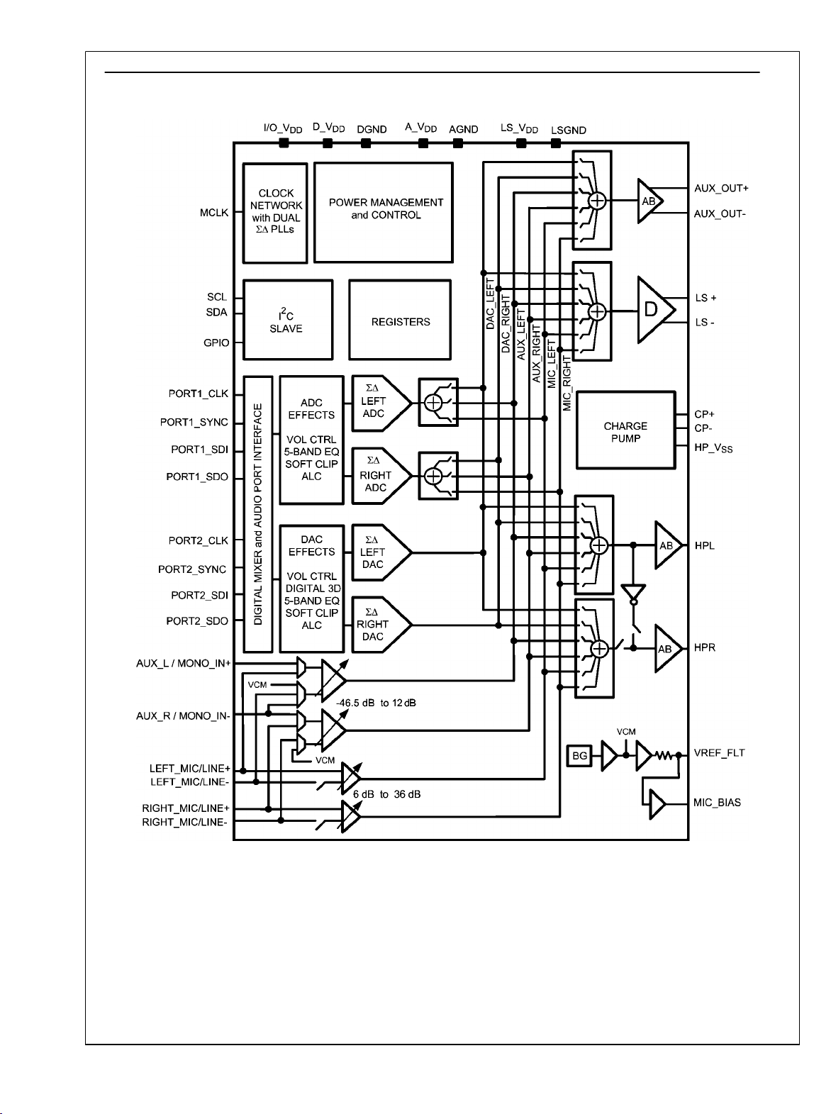
5.0 LM49350 Overview
LM49350
FIGURE 1. LM49350 Block Diagram
www.national.com 2
20194111
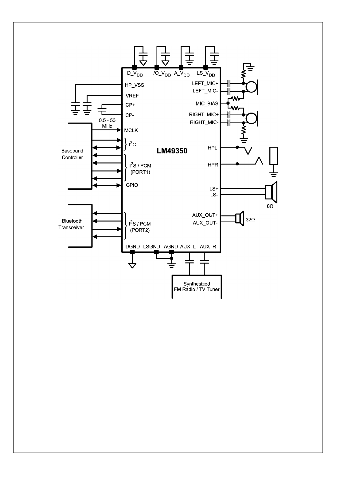
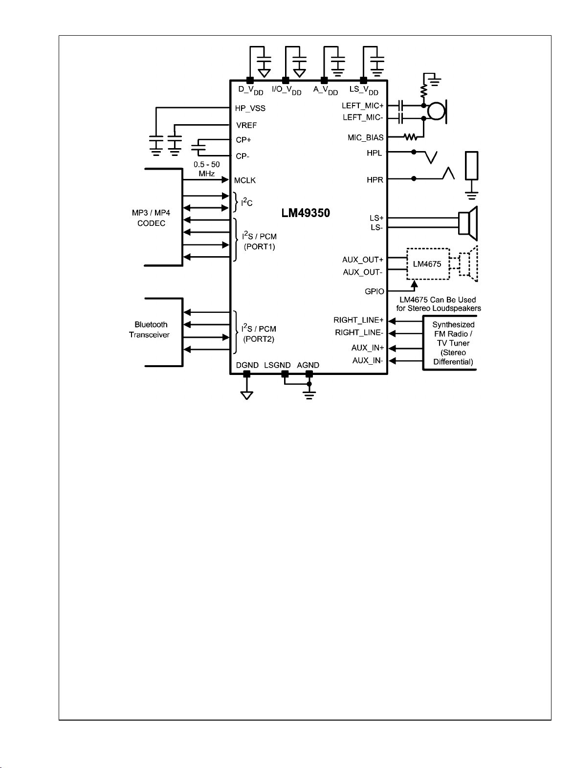
6.0 Typical Application
LM49350
20194102
FIGURE 2. Example Application in Multimedia Phone with a Dedicated Earpiece and Mono Loudspeaker
3 www.national.com
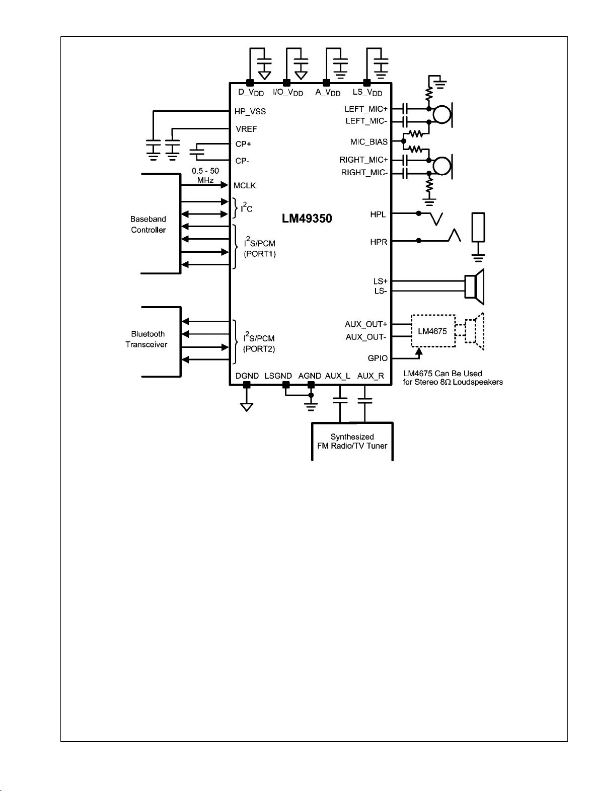
LM49350
FIGURE 3. Example Application in Multimedia Phone Using Stereo Loudspeaker
www.national.com 4
20194103
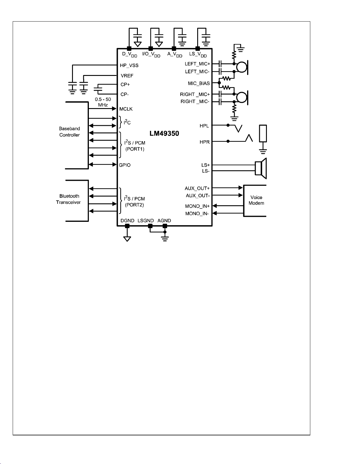
LM49350
20194104
FIGURE 4. Example Application in a Multimedia Phone Using a Dedicated RF Module for Voice Modern Functions
5 www.national.com
LM49350
20194105
FIGURE 5. Example Application in a Portable Media Player with a Differential Stereo Line Input
www.national.com 6

Table of Contents
1.0 General Description ......................................................................................................................... 1
2.0 Applications .................................................................................................................................... 1
3.0 Key Specifications ........................................................................................................................... 1
4.0 Features ........................................................................................................................................ 1
5.0 LM49350 Overview .......................................................................................................................... 2
6.0 Typical Application ........................................................................................................................... 3
7.0 Connection Diagrams ..................................................................................................................... 10
7.1 PIN TYPE DEFINITIONS .............................................................................................................. 11
8.0 Absolute Maximum Ratings ............................................................................................................ 12
9.0 Operating Ratings ......................................................................................................................... 12
10.0 Electrical Characteristics: A_VDD = LS_VDD = 3.3V; D_VDD = I/O_VDD = 1.8V (Notes 1, 2) The following
specifications apply for R
11.0 Timing Characteristics: DVDD = I/OVDD = 1.8V (Notes 1, 2) The following specifications apply for R
R
= 32Ω, f = 1kHz, unless otherwise specified. Limits apply for TA = 25°C. ...................................................... 16
L(HP)
12.0 Typical Performance Characteristics .............................................................................................. 17
13.0 System Control ............................................................................................................................ 24
13.1 I2C SIGNALS ............................................................................................................................ 24
13.2 I2C DATA VALIDITY .................................................................................................................. 24
13.3 I2C START AND STOP CONDITIONS .......................................................................................... 24
13.4 TRANSFERRING DATA ............................................................................................................. 24
13.5 I2C TIMING PARAMETERS ....................................................................................................... 26
14.0 Device Register Map .................................................................................................................... 27
15.0 Basic PMC Setup Register ............................................................................................................ 32
16.0 PMC Clocks Register ................................................................................................................... 33
17.0 PMC Clock Divide Register ........................................................................................................... 33
18.0 LM49350 Clock Network .............................................................................................................. 34
19.0 PLL Setup Registers .................................................................................................................... 36
20.0 Analog Mixer Control Registers ..................................................................................................... 41
21.0 ADC Control Registers ................................................................................................................. 47
22.0 DAC Control Registers ................................................................................................................. 49
23.0 Digital Mixer Control Registers ...................................................................................................... 50
24.0 Audio Port Control Registers ......................................................................................................... 54
25.0 Digital Effects Engine ................................................................................................................... 59
26.0 DAC Effects Registers .................................................................................................................. 77
27.0 GPIO Registers ........................................................................................................................... 95
28.0 Schematic Diagram ...................................................................................................................... 97
29.0 Demonstration Board Layout ......................................................................................................... 98
30.0 Revision History ........................................................................................................................ 101
31.0 Physical Dimensions .................................................................................................................. 102
L(LS)
= 8Ω, R
= 32Ω, f = 1kHz, unless otherwise specified. Limits apply for TA = 25°C. ......... 12
L(HP)
L(SP)
= 8Ω,
LM49350
List of Figures
FIGURE 1. LM49350 Block Diagram ............................................................................................................. 2
FIGURE 2. Example Application in Multimedia Phone with a Dedicated Earpiece and Mono Loudspeaker ......................... 3
FIGURE 3. Example Application in Multimedia Phone Using Stereo Loudspeaker ...................................................... 4
FIGURE 4. Example Application in a Multimedia Phone Using a Dedicated RF Module for Voice Modern Functions ............. 5
FIGURE 5. Example Application in a Portable Media Player with a Differential Stereo Line Input .................................... 6
List of Tables
TABLE 1. Device Register Map .................................................................................................................. 27
TABLE 2. PMC_SETUP (0x00h) ................................................................................................................. 32
TABLE 3. PMC_SETUP (0x01h) ................................................................................................................. 33
TABLE 4. PMC_SETUP (0x02h) (Default data value is 0x50h) ............................................................................. 33
TABLE 5. DAC Clock Requirements ............................................................................................................. 34
TABLE 6. ADC Clock Requirements ............................................................................................................. 34
TABLE 7. PLL_CLOCK_SOURCE (0x03h) .................................................................................................... 36
TABLE 8. PLL1_M (0x04h) ........................................................................................................................ 37
TABLE 9. PLL1_N (0x05h) ........................................................................................................................ 37
TABLE 10. PLL1_N_MOD (0x06h) .............................................................................................................. 38
TABLE 11. PLL1_P1 (0x07h) ..................................................................................................................... 38
TABLE 12. PLL1_P2 (0x08h) ..................................................................................................................... 38
TABLE 13. PLL2_M (0x09h) ...................................................................................................................... 39
TABLE 14. PLL2_N (0x0Ah) ...................................................................................................................... 39
TABLE 15. PLL2_N_MOD (0x0Bh) .............................................................................................................. 39
7 www.national.com

TABLE 16. PLL2_P (0x0Ch) ...................................................................................................................... 40
TABLE 17. CLASS_D_OUTPUT (0x10h) ....................................................................................................... 41
TABLE 18. LEFT HEADPHONE_OUTPUT (0x11h) .......................................................................................... 41
LM49350
TABLE 19. RIGHT HEADPHONE_OUTPUT (0x12h) ........................................................................................ 42
TABLE 20. AUX_OUTPUT (0x13h) .............................................................................................................. 42
TABLE 21. OUTPUT_OPTIONS (0x14h) ....................................................................................................... 43
TABLE 22. ADC_INPUT (0x15h) ................................................................................................................. 43
TABLE 23. MIC_L_INPUT (0x16h) .............................................................................................................. 43
TABLE 24. MIC_R_INPUT (0x17h) .............................................................................................................. 44
TABLE 25. AUX_L_INPUT (0x18h) .............................................................................................................. 45
TABLE 26. AUX_R_INPUT (0x19h) ............................................................................................................. 46
TABLE 27. ADC Basic (0x20h) ................................................................................................................... 47
TABLE 28. ADC_CLK_DIV (0x21h) ............................................................................................................. 47
TABLE 29. ADC TRIM (0x22h) ................................................................................................................... 48
TABLE 30. DAC Basic (0x30h) ................................................................................................................... 49
TABLE 31. DAC_CLK_DIV (0x31h) ............................................................................................................. 49
TABLE 32. Input Levels 1 (0x40h) ............................................................................................................... 51
TABLE 33. Input Levels 2 (0x41h) ............................................................................................................... 51
TABLE 34. Audio Port 1 Input (0x42h) .......................................................................................................... 52
TABLE 35. Audio Port 2 Input (0x43h) .......................................................................................................... 52
TABLE 36. DAC Input Select (0x44h) ........................................................................................................... 53
TABLE 37. Decimator Input Select (0x45h) .................................................................................................... 53
TABLE 38. BASIC_SETUP (0x50h/0x60h) ..................................................................................................... 55
TABLE 39. CLK_GEN_1 (0x51h/0x61h) ........................................................................................................ 55
TABLE 40. CLK_GEN_1 (0x52h/62h) ........................................................................................................... 56
TABLE 41. CLK_GEN_1 (0x53h/63h) ........................................................................................................... 56
TABLE 42. DATA_WIDTHS (0x54h/64h) ....................................................................................................... 57
TABLE 43. TX_MODE (0x55h/x65h) ............................................................................................................ 58
TABLE 44. ADC EFFECTS (0x70h) ............................................................................................................. 59
TABLE 45. DAC EFFECTS (0x71h) ............................................................................................................. 59
TABLE 46. HPF MODE (0x80h) .................................................................................................................. 60
TABLE 47. ADC_ALC_1 (0x81h) ................................................................................................................. 61
TABLE 48. ADC_ALC_2 (0x82h) ................................................................................................................. 62
TABLE 49. ADC_ALC_3 (0x83h) ................................................................................................................. 63
TABLE 50. ADC_ALC_4 (0x84h) ................................................................................................................. 64
TABLE 51. ADC_ALC_5 (0x85h) ................................................................................................................. 65
TABLE 52. ADC_ALC_6 (0x86h) ................................................................................................................. 66
TABLE 53. ADC_ALC_7 (0x87h) ................................................................................................................. 66
TABLE 54. ADC_ALC_8 (0x88h) ................................................................................................................. 66
TABLE 55. ADC_L_LEVEL (0x89h) ............................................................................................................. 67
TABLE 56. ADC_R_LEVEL (0x8Ah) ............................................................................................................. 68
TABLE 57. EQ_BAND_1 (0x8Bh) ................................................................................................................ 69
TABLE 58. EQ_BAND_2 (0x8Ch) ................................................................................................................ 70
TABLE 59. EQ_BAND_3 (0x8Dh) ................................................................................................................ 71
TABLE 60. EQ_BAND_4 (0x8Eh) ................................................................................................................ 72
TABLE 61. EQ_BAND_5 (0x8Fh) ................................................................................................................ 73
TABLE 62. SOFTCLIP1 (0x90h) ................................................................................................................. 74
TABLE 63. SOFTCLIP2 (0x91h) ................................................................................................................. 75
TABLE 64. SOFTCLIP3 (0x92h) ................................................................................................................. 76
TABLE 65. DAC_ALC_1 (0xA0h) ................................................................................................................ 76
TABLE 66. DAC_ALC_2 (0xA1h) ................................................................................................................ 78
TABLE 67. DAC_ALC_3 (0xA2h) ................................................................................................................ 79
TABLE 68. DAC_ALC_4 (0xA3h) ................................................................................................................ 80
TABLE 69. DAC_ALC_5 (0xA4h) ................................................................................................................ 81
TABLE 70. DAC_ALC_6 (0xA5h) ................................................................................................................ 83
TABLE 71. DAC_ALC_7 (0xA6h) ................................................................................................................ 83
TABLE 72. DAC_ALC_8 (0xA7h) ................................................................................................................ 83
TABLE 73. DAC_L_LEVEL (0xA8h) ............................................................................................................. 84
TABLE 74. DAC_R_LEVEL (0xA9h) ............................................................................................................. 85
TABLE 75. DAC_3D (0xAAh) ..................................................................................................................... 86
TABLE 76. EQ_BAND_1 (0xABh) ............................................................................................................... 87
TABLE 77. EQ_BAND_2 (0xACh) ............................................................................................................... 88
TABLE 78. EQ_BAND_3 (0xADh) ............................................................................................................... 89
TABLE 79. EQ_BAND_4 (0xAEh) ............................................................................................................... 90
TABLE 80. EQ_BAND_5 (0xAFh) ................................................................................................................ 91
TABLE 81. SOFTCLIP1 (0xB0h) ................................................................................................................. 92
TABLE 82. SOFTCLIP2 (0xB1h) ................................................................................................................. 93
TABLE 83. SOFTCLIP3 (0xB2h) ................................................................................................................. 94
TABLE 84. GPIO (0xE0h) ......................................................................................................................... 94
www.national.com 8

TABLE 85. Spread Spectrum (0xF1h) ........................................................................................................... 95
TABLE 86. ADC Compensation Filter C0 LSBs (0xF8h) ..................................................................................... 95
TABLE 87. ADC Compensation Filter C0 MSBs (0xF9h) .................................................................................... 95
TABLE 88. ADC Compensation Filter C1 LSBs (0xFAh) ..................................................................................... 96
TABLE 89. ADC Compensation Filter C1 MSBs (0xFBh) .................................................................................... 96
TABLE 90. ADC Compensation Filter C2 LSBs (0xFCh) .................................................................................... 96
TABLE 91. ADC Compensation Filter C2 MSBs (0xFDh) .................................................................................... 96
TABLE 92. AUX_LINEOUT (0xFE) .............................................................................................................. 96
LM49350
9 www.national.com
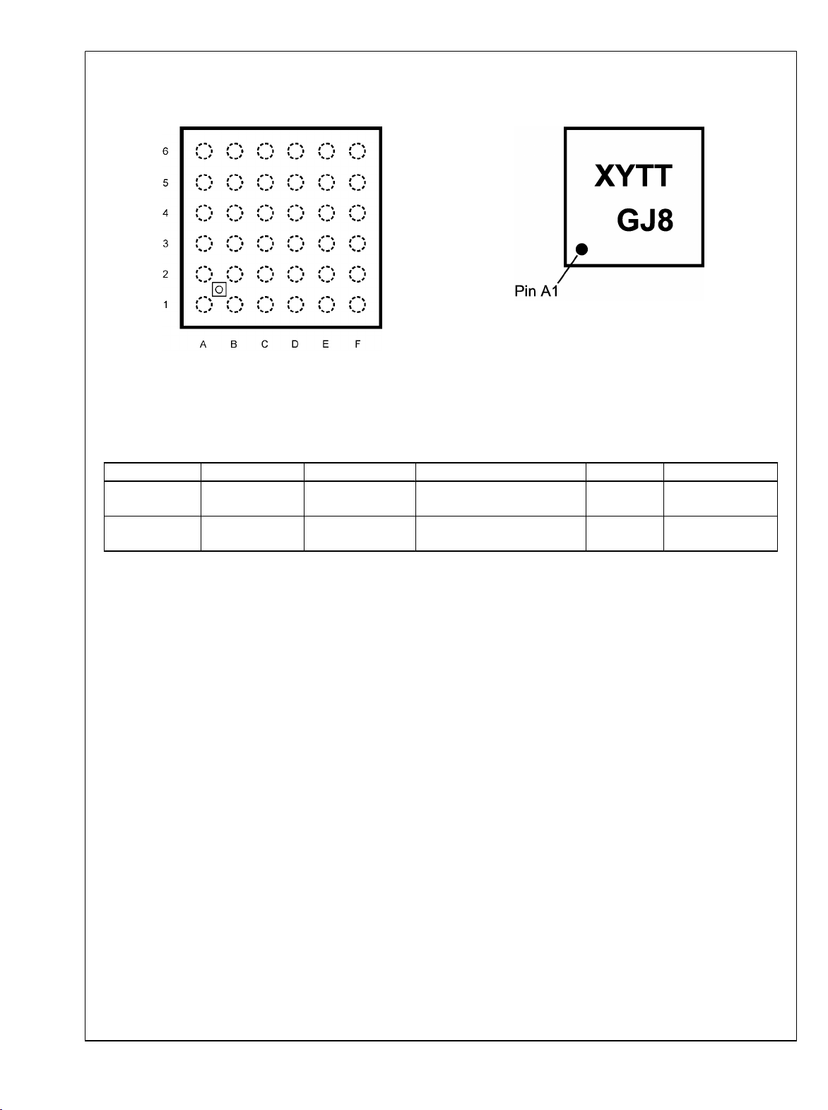
7.0 Connection Diagrams
LM49350
See NS Package Number RLA36TTA
36 Bump micro SMD
Top View (Bump Side Down)
Order Number LM49350RL
20194101
36 Bump micro SMD Marking
Top View
XY — Date Code
TT — Die Traceability
G — Boomer
J8 — LM49350RL
Ordering Information
Order Number Package Package DWG # Transport Media MSL Level Green Status
LM49350RL
LM49350RLX
36 Bump micro
SMDxt
36 Bump micro
SMDxt
RLA36TTA 250 units on tape and reel 1
RLA36TTA 3000 units on tape and reel 1
201941q7
RoHS and
no Sb/Br
RoHS and
no Sb/Br
www.national.com 10

Pin Descriptions
Pin Pin Name Type Direction Description
A1 HPR Analog Output Headphone right output
A2 A_V
DD
A3 AGND Supply Input Headphone and mixer ground
A4 VREF_FLT Analog Input/Output Filter point for the microphone power supply and internal references
A5 GPIO Digital Input/Output General purpose input or output
A6 SDA Digital Input/Output I2C interface data line
B1 HPL Analog Output Headphone left output
B2 AUX_R Analog Input Right analog input
B3 AUX_L Analog Input Left analog input
B4 PORT2_SYNC Digital Input/Output Audio Port 2 SYNC Signal (can be master or slave)
B5 PORT2_SDI Digital Input Audio Port 2 serial data input
B6 SCL Digital Input I2C interface clock line
C1 HP_V
SS
C2 AUX_OUT+ Analog Output Auxiliary positive output
C3 AUX_OUT- Analog Output Auxiliary negative output
C4 PORT2_SDO Digital Output Audio port 2 serial data out
C5 PORT2_CLK Digital Input/Output Audio port 2 clock signal (can be master or slave)
C6 MCLK Digital Input Input clock from 0.5MHz to 50 MHz
D1 CP- Analog Input/Output Charge pump flying capacitor negative input
D2 CP+ Analog Input/Output Charge pump flying capacitor positive input
D3 MIC_BIAS Analog Output Microphone ultra clean supply (2.2V)
D4 PORT1_SYNC Digital Input/Output Audio Port 1 sync signal (can be master or slave)
D5 PORT1_SDO Digital Output Audio Port 1 serial data output
D6 DGND Supply Input Digital ground
E1 LSGND Supply Input Loudspeaker ground
E2 LS_V
DD
E3 RIGHT_MIC- Analog Input Right microphone negative input
E4 LEFT_MIC- Analog Output Left microphone negative input
E5 PORT1_SDI Digital Input Audio Port 1 serial data input
E6 D_V
DD
F1 LS + Analog Output Loudspeaker positive output
F2 LS - Analog Output Loudspeaker negative output
F3 RIGHT_MIC + Analog Input Right microphone positive input
F4 LEFT_MIC + Analog Input Left microphone positive input
F5 PORT1_CLK Digital Input/Output Audio Port 1 clock signal (can be master or slave)
F6 I/O_V
DD
7.1 PIN TYPE DEFINITIONS Analog Input —
Analog Output —
Analog Input/Output —
Supply Input Headphone and mixer power supply input
Analog Output Negative power supply pin for the headphone amplifier
Supply Input Loudspeaker power supply input
Supply Input Digital power supply input
Supply Input Digital interface power supply input
vice. Passive components can be
A pin that is used by the analog
and is never driven by the device.
Supplies are part of this classification.
A pin that is driven by the device
and should not be driven by external sources.
A pin that is typically used for filtering a DC signal within the de-
Digital Input —
Digital Output —
Digital Input/Output —
connected to these pins.
A pin that is used by the digital but
is never driven by the device.
A pin that is driven by the device
and should not be driven by another device to avoid contention.
A pin that is either open drain
(SDA) or a bidirectional CMOS in/
out. In the latter case the direction
is selected by a control register
within the LM49350.
LM49350
11 www.national.com
8.0 Absolute Maximum Ratings (Notes
1, 2)
LM49350
If Military/Aerospace specified devices are required,
please contact the National Semiconductor Sales Office/
Distributors for availability and specifications.
Analog Supply Voltage
(A_VDD and LS_VDD)
Digital Supply Voltage
D_V
DD
I/O Supply Voltage
I/O_V
DD
Storage Temperature −65°C to +150°C
Power Dissipation (Note ) Internally Limited
6.0V
2.2V
5.5V
Junction Temperature 150°C
Thermal Resistance
θJA – RLA36 (soldered down
to PCB with 2in2 1oz. copper
plane) 60°C/W
Soldering Information
See Applications Note AN-1112.
9.0 Operating Ratings
Temperature Range −40°C to +85°C
Supply Voltage
A_VDD and LS_V
D_V
DD
I/O_V
DD
DD
ESD Ratings
Human Body Model (Note )
Machine Model (Note )
2000V
200V
10.0 Electrical Characteristics: A_VDD = LS_VDD = 3.3V; D_VDD = I/O_VDD = 1.8V
(Notes 1, 2) The following specifications apply for R
for TA = 25°C.
Symbol Parameter Conditions
DC CHARACTERISTICS (Digital current combines D_VDD and I/O_VDD. Analog current combines A_VDD and LS_VDD)
DI
DI
SD
ST
Digital Shutdown Current
Digital Standby Current
Shutdown Mode,
f
f
f
Digital Active Current (MP3 Mode)
Stereo DAC On, OSR
PLL Off, HP On
Digital Active Current (FM Mode) f
Analog Audio modes
DI
DD
Digital Active Current (FM Record
Mode)
f
Stereo ADC On, OSR
PLL Off, Stereo Analog Inputs On
Digital Active Current (CODEC
Mode)-
f
Mono ADC On, Stereo DAC On,
OSR = 128, PLL Off, MIC On
AI
SD
AI
ST
Analog Shutdown Current Shutdown Mode 0.3 5
Analog Standby Quiescent Current Reference Voltages On only 0.85 1.5 mA (max)
f
Analog Supply Current (MP3 Mode)
Stereo DAC On, OSR
PLL Off, HP On
Analog Supply Current (FM Mode) Stereo Analog Inputs On, HP On 5.3 7 mA (max)
AI
DD
PLLI
HPI
LSI
DD
DD
DD
Analog Supply Current (FM Record
Mode)
Analog Supply Current (CODEC
Mode)
PLL Total Active Current
Headphone Quiescent Current Stereo HP On only 3.5 mA
Loudspeaker Quiescent Current LS On only 2.9 mA
f
Stereo ADC On, OSR
PLL Off, Stereo Analog Inputs On
f
Mono ADC On, Stereo DAC On,
OSR = 128, PLL Off, MIC On
f
f
= 8Ω, R
L(LS)
= 13MHz, PLL Off
MCLK
= 12.288MHz, PMC On only
MCLK
= 11.2896MHz, fS = 44.1kHz,
MCLK
= 13MHz
MCLK
= 12.288MHz, fS = 48kHz,
MCLK
= 11.2896MHz, fS = 44.1kHz,
MCLK
= 11.2896MHz, fS = 44.1kHz,
MCLK
= 12.288MHz, fS = 48kHz,
MCLK
= 11.2896MHz, fS = 44.1kHz,
MCLK
= 13MHz,
MCLK
= 12MHz, PLL On only
PLLOUT
= 32Ω, f = 1kHz, unless otherwise specified. Limits apply
L(HP)
DAC
ADC
DAC
ADC
= 128,
= 128,
= 128,
= 128,
LM49350
Typical
(Note 6)
Limit
(Note 7)
2 15 µA (max)
0.25 1 mA (max)
0.9 2 mA (max)
0.2 0.5 mA (max)
1.5 2 mA (max)
2.7 3.8 mA (max)
7.8 10 mA (max)
9.8 12 mA (max)
13 15 mA (max)
2.9 5.5 mA (max)
2.7V to 5.5V
1.7V to 2.0V
1.6V to 4.5V
Units
(Limits)
μA (max)
www.national.com 12
LM49350
Symbol Parameter Conditions
MICI
DD
ADCI
DD
DACI
DD
AUXINI
AUXOUTI
Microphone Quiescent Current mono MIC + MIC Bias On 0.5 mA
ADC Total Active Current
DAC Total Active Current
Auxiliary Input Amplifier Quiescent
DD
Current
Auxiliary Output Amplifier Quiescent
DD
Current
fS = 48kHz, Stereo
fS = 48kHz, Stereo
Stereo Auxiliary Inputs enabled 0.7 mA
AUX_LINE_OUT enabled 0.5 mA
Earpiece mode enabled 1.0 mA
LOUDSPEAKER AMPLIFIER
LS
EFF
THD+N Total Harmonic Distortion + Noise
Loudspeaker Efficiency
PO = 400mW, RL = 8Ω
PO = 400mW, f = 1kHz,
RL = 8Ω, Mono Input Signal
RL = 8Ω, f = 1kHz, THD+N = 1%,
P
O
Output Power
Mono Input Signal
RL = 4Ω, f = 1kHz, THD+N = 1%,
Mono Input Signal
V
= 200mV
PSRR Power Supply Rejection Ration
SNR Signal-to-Noise Ratio
RIPPLE
f
= 217Hz
RIPPLE
Mono Input Terminated
V
= 1.0μF
REF
Reference = V
Gain = 0dB, A-weighted
P-P
OUT
Mono Input Terminated
e
OS
V
OS
T
WU
Output Noise
Offset Voltage Gain = 0dB, form Mono Input 10 50 mV (max)
Turn-On Time PMC Clock = 300kHz 28 ms
Gain = 0dB, A-weighted,
Mono Input Terminated
HEADPHONE AMPLIFIERS
PO = 7.5mW, f = 1kHz,
THD+N Total Harmonic Distortion + Noise
RL = 32Ω
Stereo Analog Input Signal
P
O
Headphone Output Power
PSRR Power Supply Rejection Ratio
RL = 32Ω, f = 1kHz, THD+N = 1%,
Stereo Analog Input Signal
V
= 200mV
RIPPLE
P-P
Stereo Analog Inputs Terminated,
V
= 1.0μF, Mono Differential Input
REF
Mode
Reference = V
OUT
Gain = 0dB, A-weighted
SNR Signal-to-Noise Ratio
Stereo Inputs Terminated
Reference = V
OUT
0dB,
A-weighted, I2S Input = Digital Zero
Gain = 0dB, A-weighted,
e
OS
Output Noise
Stereo Inputs Terminated
Gain = 0dB, A-weighted,
I2S Input = Digital Zero
PO = 60mW, f = 1kHz,
X
TALK
Crosstalk
RL = 32Ω
Stereo Analog Input Signal
(1% THD+N )
, f
RIPPLE
= 217Hz
(1% THD+N )
(0dBFS ) Gain =
LM49350
Typical
(Note 6)
Limit
(Note 7)
Units
(Limits)
9 mA
5.5 mA
83 %
0.07 %
495 400 mW (min)
800 mW
73 55 dB (min)
95 85 dB (min)
35 µV
0.025 0.1 % (max)
69 60 mW (min)
97 75 dB (min)
106 98 dB (min)
96 90 dB (min)
8 µV
16 µV
71 dB
13 www.national.com
Symbol Parameter Conditions
LM49350
ΔA
CH-CH
V
OS
T
WU
AUXILIARY OUTPUTS
THD+N Total Harmonic Distortion + Noise
P
OUT
PSRR Power Supply Rejection Ratio
SNR Signal-to-Noise Ratio
∈
OUT
V
OS
T
WU
STEREO ADC
THD+N
PB
ADC
R
ADC
SNR
ADC
ADC
LEVEL
STEREO DAC
THD+N
DAC
LEVEL
Channel-to-Channel Gain Matching
AUX Gain = 0dB
Output Offset Voltage
From Differential Mono Input
DAC Gain = 0dB, From DAC Input
f
= 12.288MHz, PLL off
MCLK
Turn-On Time PMC Clock = 300kHz 28 ms
AUX_LINE_OUT
RL = 5kΩ, V
Earpiece mode, f = 1kHz
RL = 32Ω BTL, P
Output Power
Earpiece mode, f = 1kHz
RL = 32Ω BTL, THD+N = 1%
V
= 200mV
RIPPLE
Mono Input terminated, C
AUX_LINE_OUT
V
= 200mV
RIPPLE
Mono Input terminated, C
Earpiece mode
Gain = 0dB, V
A-weighted, Mono Input Terminated
Output Noise
Gain = 0dB, V
A-weighted, Mono Input Terminated
Gain = 0dB, From Mono Input
Output Offset Voltage
AUX_LINE_OUT
Gain = 0dB, From Mono Input
Earpiece mode
Turn-On Time PMC Clock = 300kHz 28 ms
ADC Total Harmonic Distortion +
ADC
Noise
Differential Line Input
VIN = 200mV
Gain = 0dB
HPF On, fS = 48kHz
ADC Passband
Lower -3dB Point
HPF On, Upper -3dB Point
ADC Ripple ADC Compensated 0.1 dB
Reference = V
6dB,
A-weighted From MIC, fS = 8kHz
ADC Signal-to-Noise Ratio
Reference = V
0dB,
A-weighted From Stereo Input, fS =
48kHz
ADC Full Scale Input Level
DAC Total Harmonic Distortion +
DAC
Noise
I2S Input
VIN = 500mFFS
Gain = 0dB
DAC Full Scale Output Level
= 1V
OUT
RMS
= 20mW
OUT
, f
P-P
, f
P-P
= V
REF
= V
REF
, f = 1kHz
RMS
(0dBFS ) Gain =
OUT
(0dBFS ) Gain =
OUT
, f = 1kHz
RMS
= 217Hz
RIPPLE
= 1μF
REF
= 217Hz
RIPPLE
= 1μF
REF
(1%THD+N)
OUT
(1%THD+N)
OUT
LM49350
Typical
(Note 6)
Limit
(Note 7)
Units
(Limits)
0.03 dB
0.5 6 mV (max)
1 6 mV (max)
0.004 %
0.08 %
58 45 mW (min)
100 dB
94 62 dB (min)
100 dB
13
7 mV
3 15 mV (max)
0.03 %
300 Hz
0.41*f
S
kHz
90 dB
94 dB
1
V
0.05 %
1
V
μV
RMS
RMS
www.national.com 14
LM49350
Symbol Parameter Conditions
R
DAC
PB
SNR
DAC
DAC
DAC Ripple
DAC Passband Upper –3dB Point 0.45*f
DAC Signal-to-Noise Ratio fS = 48kHz, A-weighted
LM49350
Typical
(Note 6)
Limit
(Note 7)
0.1 dB
S
kHz
96 dB
Units
(Limits)
MIC BIAS
V
BIAS
Microphone Bias Voltage MIC input selected 2.2 V
VOLUME CONTROL
VCR
AUX
VCR
DAC
VCR
ADC
VCR
MIC
SS
AUX
SS
DAC
SS
ADC
SS
MIC
SV
AUX
SV
MIC
Note 1: “Absolute Maximum Ratings” indicate limits beyond which damage to the device may occur, including inoperability and degradation of device reliability
and/or performance. Functional operation of the device and/or non-degradation at the Absolute Maximum Ratings or other conditions beyond those indicated in
the Recommended Operating Conditions is not implied. The Recommended Operating Conditions indicate conditions at which the device is functional and the
device should not be operated beyond such conditions. All voltages are measured with respect to the ground pin, unless otherwise specified.
Note 2: The Electrical Characteristics tables list guaranteed specifications under the listed Recommended Operating Conditions except as otherwise modified
or specified by the Electrical Characteristics Conditions and/or Notes. Typical specifications are estimations only and are not guaranteed.
Note 3: The maximum power dissipation must be derated at elevated temperatures and is dictated by T
allowable power dissipation is P
Note 4: Human body model, applicable std. JESD22-A114C.
Note 5: Machine model, applicable std. JESD22-A115-A.
Note 6: Typical values represent most likely parametric norms at TA = +25ºC, and at the Recommended Operation Conditions at the time of product
characterization and are not guaranteed.
Note 7: Datasheet min/max specification limits are guaranteed by test or statistical analysis.
Stereo Input Volume Control Range
DAC Volume Control Range
ADC Volume Control Range
MIC Volume Control Range
AUX Volume Control Stepsize 1.5 dB
DAC Volume Control Stepsize 1.5 dB
DAC Volume Control Stepsize 1.5 dB
MIC Volume Control Stepsize 2 dB
AUX Volume Setting Variation ±1 dB (max)
MIC Volume Setting Variation ±1 dB (max)
= (T
DMAX
- TA) / θJA or the number given in Absolute Maximum Ratings, whichever is lower.
JMAX
Minimum Gain –46.5 dB
Maximum Gain 12 dB
Minimum Gain –76.5 dB
Maximum Gain 18 dB
Minimum Gain –76.5 dB
Maximum Gain 18 dB
Minimum Gain 6 dB
Maximum Gain 36 dB
, θJA, and the ambient temperature, TA. The maximum
JMAX
15 www.national.com
11.0 Timing Characteristics: DVDD = I/OVDD = 1.8V (Notes 1, 2) The following specifications
apply for R
LM49350
Symbol Parameter Conditions
PLL
f
IN
DIGITAL AUDIO INTERFACE TIMING
t
BCLKR
t
BCLKCF
t
BCLKDS
t
DL
t
DST
t
DHT
CONTROL INTERFACE TIMING
1
2 Clock Low Time
3 Clock High Time 600 ns (min)
4 Setup Time for a Repeated START
5 Data Hold Time
6 Data Setup Time 100 ns (min)
7 Rise Time of SDA and SCL
8 Fall Time SDA and SCL
9 Setup Time for STOP Condition 600 ns (min)
10
C
B
L(SP)
= 8Ω, R
= 32Ω, f = 1kHz, unless otherwise specified. Limits apply for TA = 25°C.
L(HP)
LM49350
PLL Input Frequency Range
BCK rise time
BCK fall time
BCK duty cycle
WS Propagation Delay from BCK
falling edge
DATA Setup Time to BCK Rising Edge
DATA Hold Time from BCK Rising
Edge
Typical
(Note 6)
Minimum MCLK Frequency 0.5 MHz (min)
Maximum MCLK Frequency 50 MHz (max)
3 ns (max)
50 %
10 ns (max)
10 ns (min)
10 ns (min)
Limit
(Note 7)
3 ns (max)
SCL Frequency 400 kHz (max)
Hold Time (repeated START
Condition)
0.6
1.3
Condition
Bus Free Time Between a STOP and
START Condition
Bus Capacitance
600 ns (min)
Output
Input
1.3
300
900
0
900
20+0.1C
300
15+0.1C
300
B
B
10
200
Units
(Limits)
μs (min)
μs (min)
ns (min)
ns (max)
ns (min)
ns (max)
ns (min)
ns (max)
ns (min)
ns (max)
μs (min)
pF (min)
pF(max)
www.national.com 16
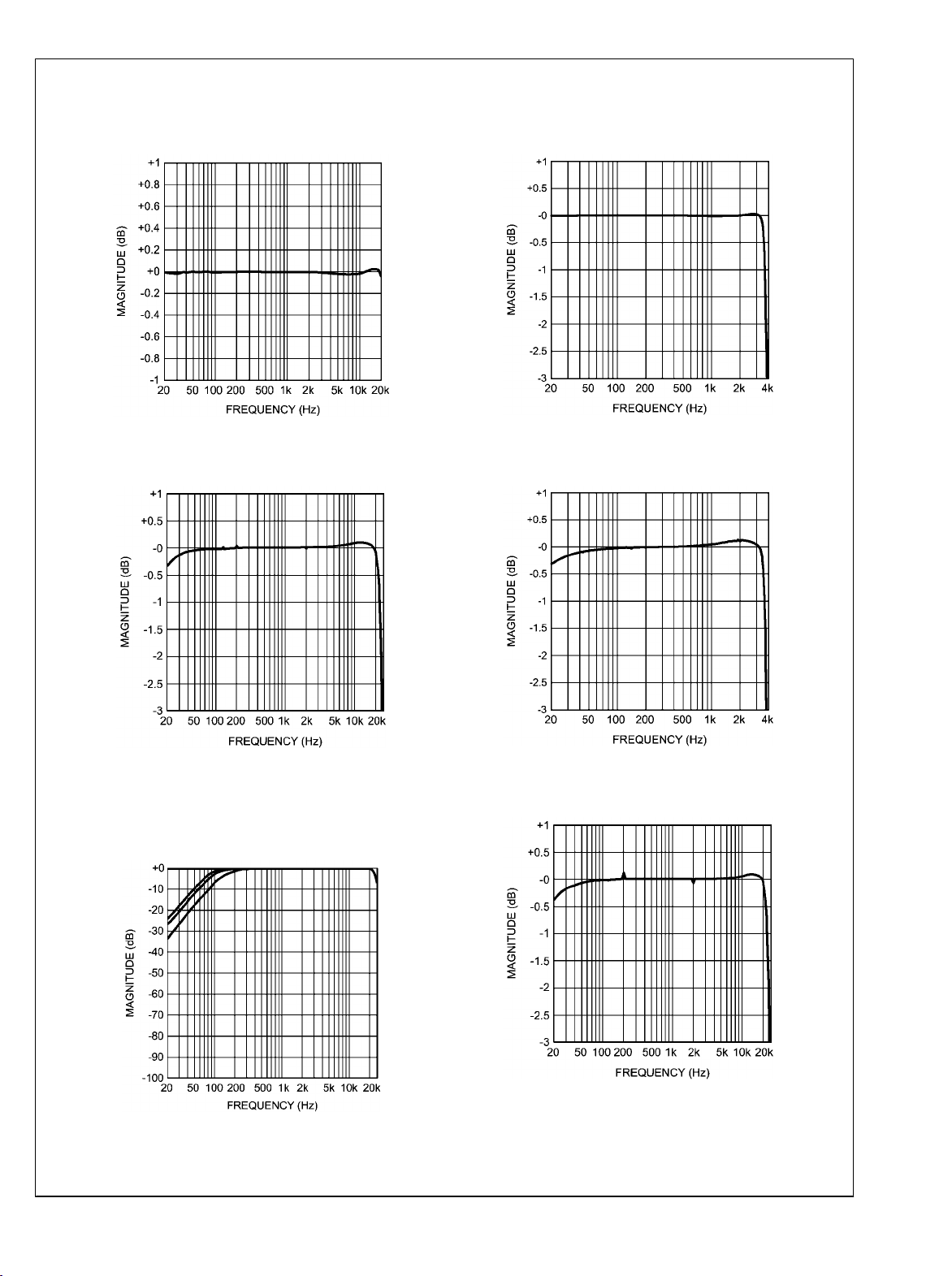
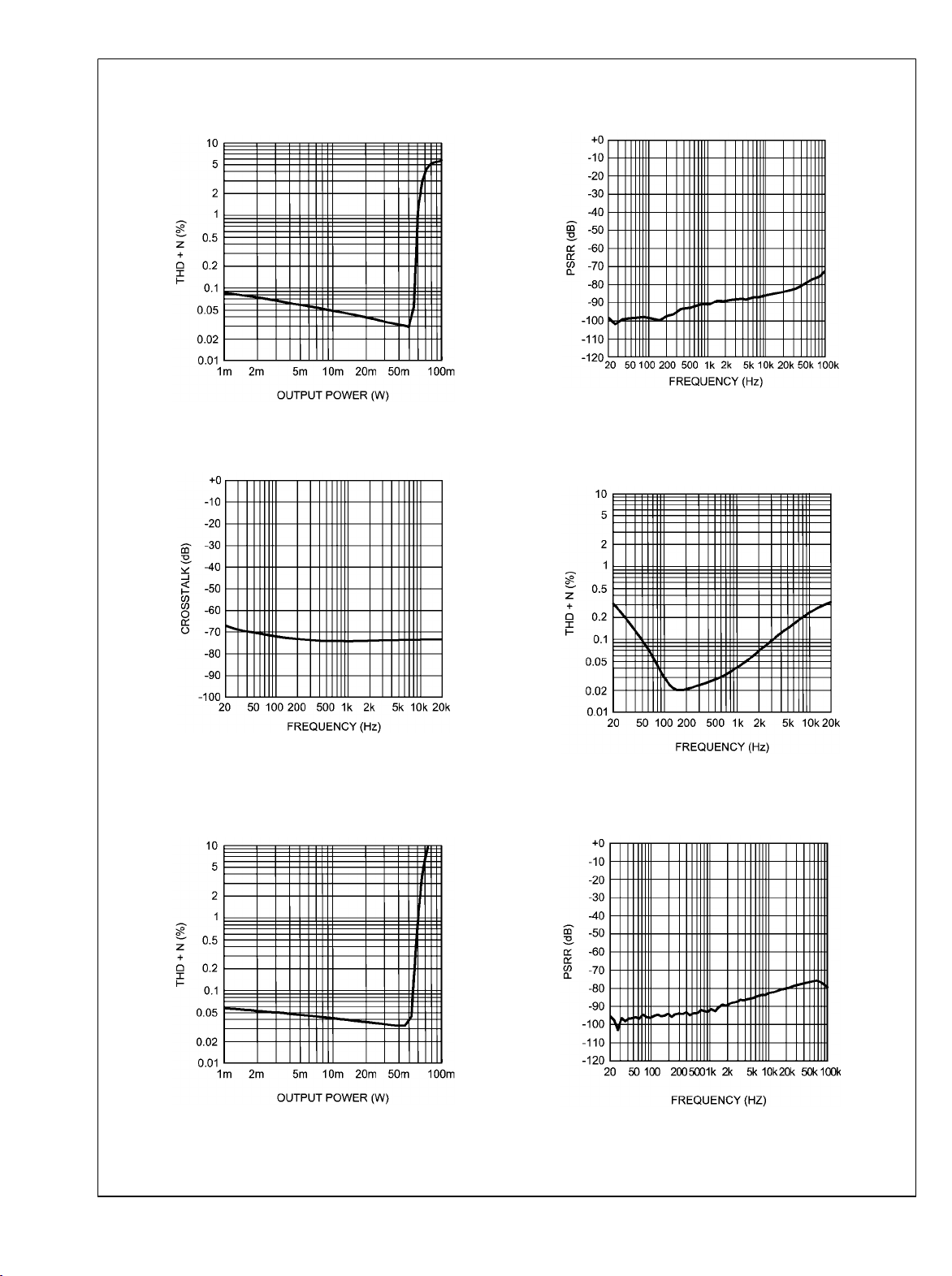
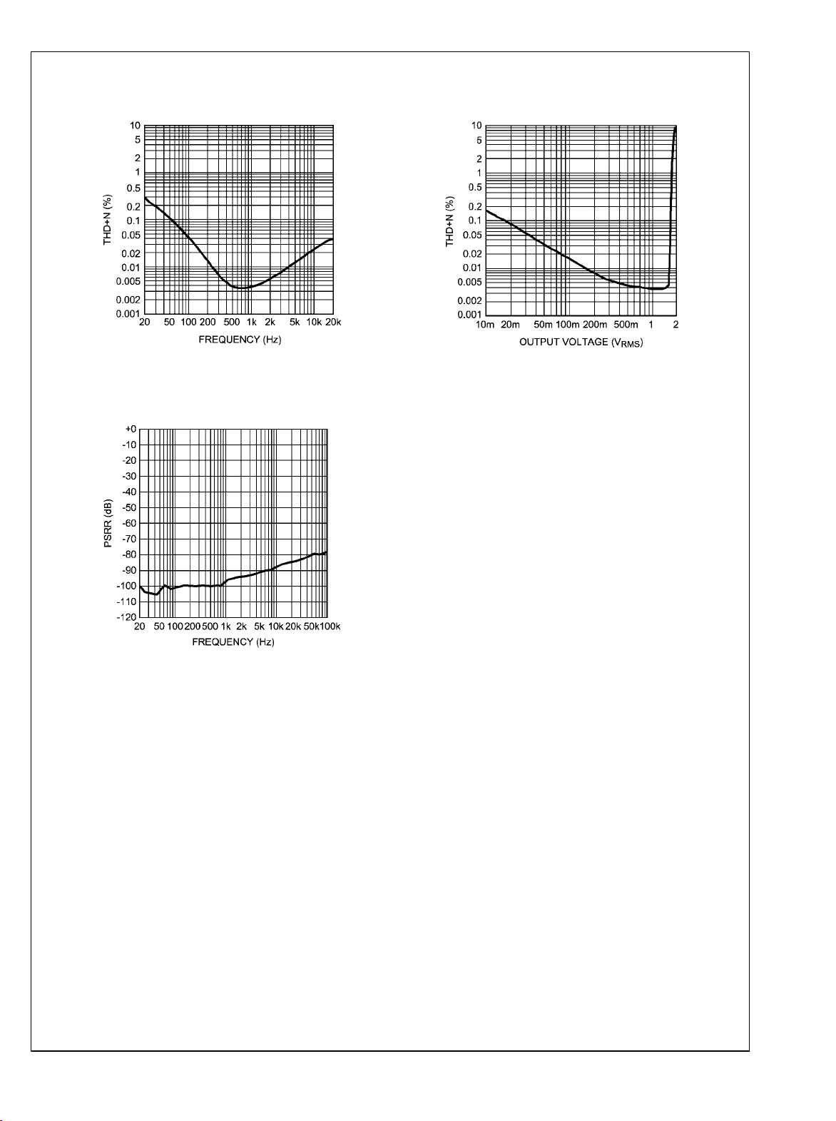
12.0 Typical Performance Characteristics
LM49350
DAC Frequency Response
fS = 48kHz, OSR = 128
20194139
Stereo Audio ADC Frequency Response
fS = 48kHz, OSR = 128, CIN = 1μF, MIC gain = 6dB
DAC Frequency Response
fS = 8kHz, OSR = 128
20194140
Stereo Audio ADC Frequency Response
fS = 8kHz, OSR = 128, CIN = 1μF, MIC gain = 6dB
20194141
Stereo Audio ADC HPF Frequency Response
fS = 48kHz, OSR = 128, CIN = 1μF, MIC gain = 6dB
(Top-No HPF, Upper-HPF_Mode = '101',
Lower-HPF_Mode = '110)'
Bottom-HPF_Mode = '111'
20194143
20194142
Mono Voice ADC Frequency Response
fS = 48kHz, OSR = 128, CIN = 1μF, MIC gain = 6dB
20194144
17 www.national.com
LM49350
Mono Voice ADC Frequency Response
fS = 8kHz, OSR = 128, CIN = 1μF, MIC gain = 6dB
20194145
Mono Voice ADC HPF Frequency Response
fS = 48kHz, OSR = 128, CIN = 1μF, MIC gain = 6dB
(Top-No HPF)
(From Left to Right:
HPF_Mode = '000', '001', '010', '011', '100')
20194146
Mono Voice ADC HPF Frequency Response
fS = 8kHz, OSR = 128, CIN = 1μF, MIC gain = 6dB
(Top-No HPF)
(From Left to Right:
HPF_Mode = '000', '001', '010', '011', '100')
20194147
ADC Output THD+N vs Frequency
Differential MIC Input, MIC Gain = 6dB
VIN = 100mV
, fS = 48kHz
RMS
ADC Output THD+N vs Frequency
Differential Line Input, Aux Gain = 0dB
VIN = 200mV
ADC Output THD+N vs V
Differential Line Input, Aux Gain = 0dB
, fS = 48kHz
RMS
20194155
IN
VIN = 1kHz, fS = 48kHz
20194156
www.national.com 18
20194148
LM49350
ADC Output THD+N vs V
Differential MIC Input, MIC Gain = 6dB
IN
VIN = 1kHz, fS = 48kHz
20194149
Loudspeaker THD+N vs Frequency
Differential Aux Input, Aux Gain = 0dB
VDD = 5V, P
= 400mW, RL = 8Ω
OUT
Loudspeaker THD+N vs Frequency
Differential Aux Input, Aux Gain = 0dB
VDD = 3.3V, P
= 400mW, RL = 8Ω
OUT
20194159
Loudspeaker THD+N vs Frequency
Differential Aux Input, Aux Gain = 0dB
LS_VDD = 3.3V, P
= 500mW, RL = 4Ω
OUT
20194161
Loudspeaker THD+N vs Output Power
Differential Aux Input, Aux Gain = 0dB
VDD = 3.3V, VIN = 1kHz, RL = 8Ω
20194165
20194181
Loudspeaker THD+N vs Output Power
Differential Aux Input, Aux Gain = 0dB
VDD = 4.2V, VIN = 1kHz, RL = 8Ω
20194166
19 www.national.com
LM49350
Loudspeaker THD+N vs Output Power
Differential Aux Input, Aux Gain = 0dB
VDD = 5V, VIN = 1kHz, RL = 8Ω
Loudspeaker THD+N vs Output Power
Differential Aux Input, Aux Gain = 0dB
LS_VDD = 3.3V, RL = 4Ω, f = 1kHz
20194167
Loudspeaker THD+N vs Output Power
Differential Aux Input, Aux Gain = 0dB
LS_VDD = 4.2V, RL = 4Ω, f = 1kHz
20194183
Loudspeaker PSRR vs Frequency
LS_VDD = 3.3V, Aux Gain = 0dB
Differential Aux Input to Ground
V
= 200mV
RIPPLE
PP
20194182
Loudspeaker THD+N vs Output Power
Differential Aux Input, Aux Gain = 0dB
LS_VDD = 5V, RL = 4Ω, f = 1kHz
20194184
Loudspeaker PSRR vs Frequency
LS_VDD = 4.2V, Aux Gain = 0dB
Differential Aux Input to Ground
V
= 200mV
RIPPLE
PP
20194151
www.national.com 20
20194152
LM49350
Loudspeaker PSRR vs Frequency
LS_VDD = 5V, Aux Gain = 0dB
Differential Aux Input to Ground
V
= 200mV
RIPPLE
PP
Headphone THD+N vs Frequency
Stereo Aux Input, Aux Gain = 0dB
VDD = 5V, P
= 7.5mW, RL = 32Ω
OUT
20194153
Headphone THD+N vs Frequency
Stereo Aux Input, Aux Gain = 0dB
VDD = 3.3V, P
= 7.5mW, RL = 32Ω
OUT
20194157
Headphone THD+N vs Frequency
Differential Aux Input, Aux Gain = 0dB
A_VDD = 3.3V, P
= 7.5mW, RL = 16Ω
OUT
20194158
Headphone THD+N vs Output Power
Stereo Aux Input, Aux Gain = 0dB
VDD = 3.3V, VIN = 1kHz, RL = 32Ω
20194173
20194179
Headphone THD+N vs Output Power
Stereo Aux Input, Aux Gain = 0dB
VDD = 5V, VIN = 1kHz, RL = 32Ω
20194174
21 www.national.com
LM49350
Headphone THD+N vs Output Power
A_VDD = 3.3V, Stereo Aux Input, Aux Gain = 0dB
RL = 16Ω, f = 1kHz
Differential Aux Input to Ground, Aux Gain = 0dB
Headphone PSRR vs Frequency
V
= 200mV
RIPPLE
PP
20194180
Headphone Crosstalk vs Frequency
Stereo Aux Inputs, Aux Gain = 0dB, RL = 32Ω
20194169
Earpiece THD+N vs Output Power
Differential Aux Input, Aux Gain = 0dB
A_VDD45 = 3.3V, RL = 32Ω, f = 1kHz
20194175
Earpiece THD+N vs Frequency
Differential Aux Input, Aux Gain = 0dB
A_VDD = 3.3V, P
= 20mW, RL = 32Ω
OUT
20194176
Earpiece PSRR vs Frequency
Differential Aux Input to Ground, Aux Gain = 0dB
V
= 200mV
RIPPLE
PP
20194177
www.national.com 22
20194178
LM49350
AUXOUT THD+N vs Frequency
Differential Aux Input, Aux Gain = 0dB
VDD = 5V, V
OUT
= 1V
, RL = 5kΩ
RMS
20194162
AUXOUT PSRR vs Frequency
Differential Aux Input to Ground, Aux Gain = 0dB
V
= 200mV
RIPPLE
PP
AUXOUT THD+N vs Output Voltage
Differential Aux Input, Aux Gain = 0dB
V
= 1kHz, RL = 5kΩ
IN
20194168
20194154
23 www.national.com
13.0 System Control
Method 1. I2C Compatible Interface
LM49350
13.1 I2C SIGNALS
In I2C mode the LM49350 pin SCL is used for the I2C clock
SCL and the pin SDA is used for the I2C data signal SDA. Both
these signals need a pull-up resistor according to I2C specification. The I2C slave address for LM49350 is 00110102.
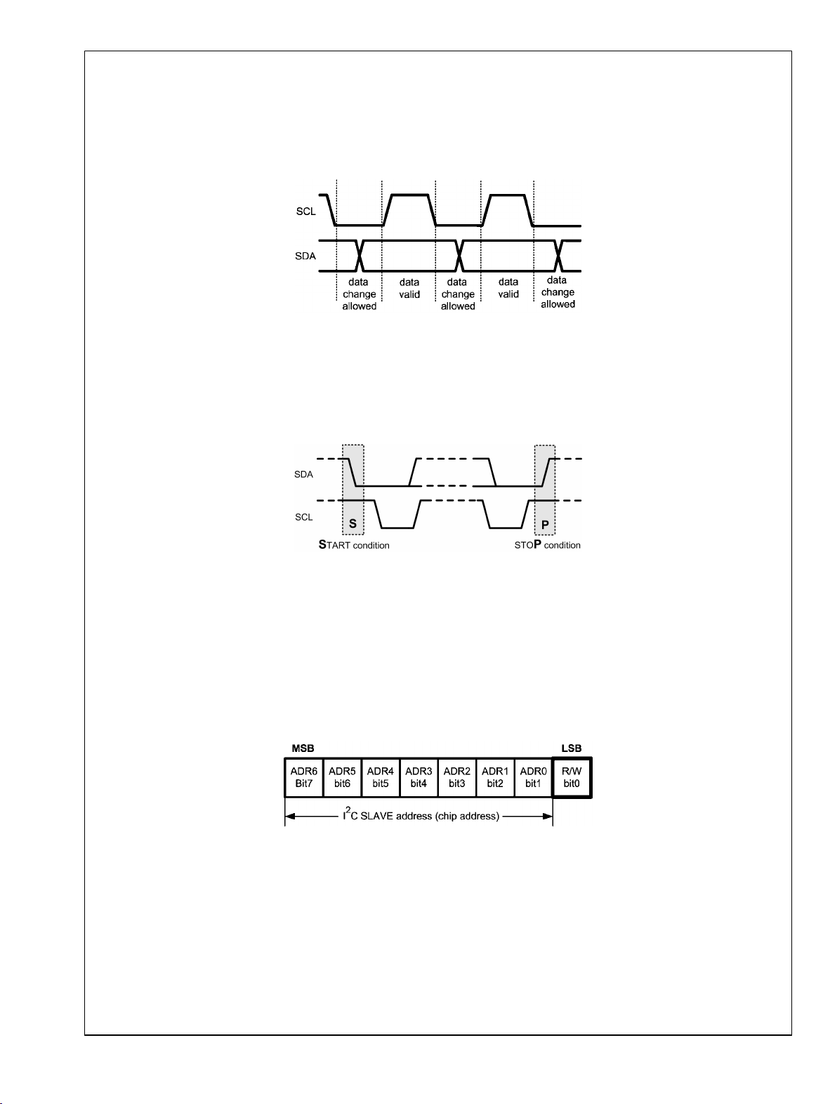
13.2 I2C DATA VALIDITY
The data on SDA line must be stable during the HIGH period
of the clock signal (SCL). In other words, state of the data line
can only be changed when SCL is LOW.
FIGURE 6: I2C Signals: Data Validity
13.3 I2C START AND STOP CONDITIONS
START and STOP bits classify the beginning and the end of
the I2C session. START condition is defined as SDA signal
transitioning from HIGH to LOW while SCL line is HIGH.
STOP condition is defined as the SDA transitioning from LOW
to HIGH while SCL is HIGH. The I2C master always generates
FIGURE 7: I2C Start and Stop Conditions
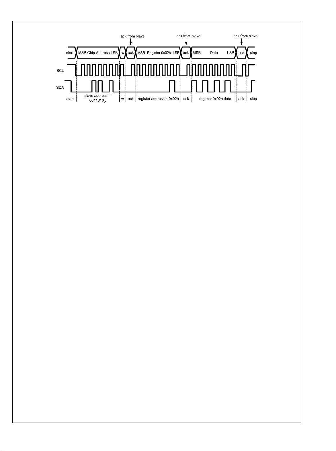
13.4 TRANSFERRING DATA
Every byte put on the SDA line must be eight bits long, with
the most significant bit (MSB) being transferred first. Each
byte of data has to be followed by an acknowledge bit. The
acknowledge related clock pulse is generated by the master.
The transmitter releases the SDA line (HIGH) during the acknowledge clock pulse. The receiver must pull down the SDA
line during the 9th clock pulse, signifying an acknowledge. A
receiver which has been addressed must generate an acknowledge after each byte has been received.
20194123
START and STOP bits. The I2C bus is considered to be busy
after START condition and free after STOP condition. During
data transmission, I2C master can generate repeated START
conditions. First START and repeated START conditions are
equivalent, function-wise.
20194124
After the START condition, the I2C master sends a chip address. This address is seven bits long followed by an eight bit
which is a data direction bit (R/W). The LM49350 address is
00110102. For the eighth bit, a “0” indicates a WRITE and a
“1” indicates a READ. The second byte selects the register to
which the data will be written. The third byte contains data to
write to the selected register.
FIGURE 8: I2C Chip Address
Register changes take effect at the SCL rising edge during
the last ACK from slave.
www.national.com 24
20194125
LM49350
w = write (SDA = “0”)
r = read (SDA = “1”)
ack = acknowledge (SDA pulled down by slave)
rs = repeated start
20194126
FIGURE 9: Example I2C Write Cycle
25 www.national.com
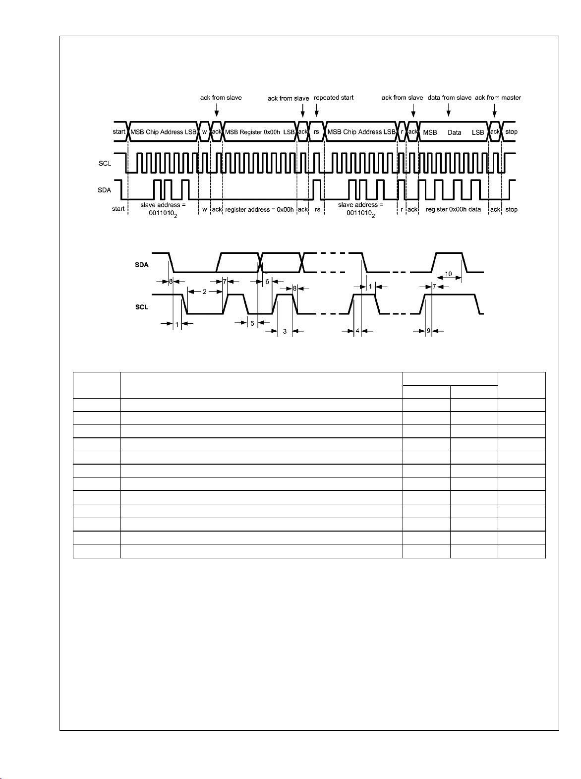
When a READ function is to be accomplished, a WRITE function must precede the READ function, as shown in the Read Cycle
waveform.
LM49350
FIGURE 10: Example I2C Read Cycle
FIGUREW 11: I2C Timing Diagram
20194128
20194127
13.5 I2C TIMING PARAMETERS
Symbol Parameter Limit Units
Min Max
1 Hold Time (repeated) START Condition 0.6 µs
2 Clock Low Time 1.3 µs
3 Clock High Time 600 ns
4 Setup Time for a Repeated START Condition 600 ns
5 Data Hold Time (Output direction, delay generated by LM49350) 300 900 ns
5 Data Hold Time (Input direction, delay generated by the Master) 0 900 ns
6 Data Setup Time 100 ns
7 Rise Time of SDA and SCL 20+0.1C
8 Fall Time of SDA and SCL 15+0.1C
b
b
300 ns
300 ns
9 Set-up Time for STOP condition 600 ns
10 Bus Free Time between a STOP and a START Condition 1.3 µs
C
NOTE: Data guaranteed by design
Capacitive Load for Each Bus Line 10 200 pF
b
www.national.com 26

14.0 Device Register Map
TABLE 1. Device Register Map
Address Register 7 6 5 4 3 2 1 0
BASIC SETUP
0x00h PMC CHIP PORT2 PORT1 MCLK OSC PLL2 PLL1 CHIP
SETUP ACTIVE CLK OVR CLK OVR OVR ENB ENB ENB ENABLE
0x01h PMC
CLOCKS
0x02h PMC
CLK_DIV
0x03h PLL2_CLK_SEL PLL1_CLK_SEL
0x04h PLL1 M PLL1 M
0x05h PLL1 N PLL1 N
0x06h PLL1
N_MOD
0x07h PLL1 P1 PLL1 P1 [7:0]
0x08h PLL1 P2 PLL1 P2[7:0]
0x09h PLL2 M PLL2 M
0x0Ah PLL2 N PLL2 N
0x0Bh PLL2
N_MOD
0x0Ch PLL2 P PLL2 P[7:0]
0x10h CLASSD AUXR_LS AUXL_LS MICR_LS MICL_LS DACR_LS DACL_LS
0x11h HEAD
PHONESL
0x12h HEAD AUXR_HPRAUXL_HPRMICR_HPRMICL_HPR DACR_HPRDACL_HP
PHONESR
0x13h AUX_OUT AUXR_AX AUXL_AX MICR_AX MICL_AX DACR_AX DACL_AX
0x14h OUTPUT
OPTIONS
0x15h ADC AUXR_ADCRAUXL_ADCLMICR_ADCRMICL_ADCLDACR_ADCRDACL_AD
0x16h MICL_LVL MUTE SE/DIFF MIC_L_LEVEL
0x17h MICR_LVL MUTE SE/DIFF MIC_R_LEVEL
0x18h AUXL_LVL FROM
0x19h AUXR_LVLDIFF_MODEFROM
0x20h ADC
BASIC
0x21h ADC
CLOCK
0x22h ADC_DSP ADC_TRI
0x30h DAC_BASICDSPONLY DAC_CLK_SEL MUTE_R MUTE_L DAC_OSR
PMC_CLK_SEL
PMC_CLK_DIV(R)
PLLs
PLL2 P2[8] PLL1 P1[8] PLL1 N_MOD
PLL2 P[8] PLL2 N_MOD
ANALOG MIXER
AUXR_HPLAUXL_HPLMICR_HPL MICL_HPL DACR_HPLDACL_HP
LSSHORT
IGNORE
DSPONLY ADC_CLK_SEL MUTE_R MUTE_L ADC_OSR MONO
LSTHERM
IGNORE
LINEL
LINER
HPTHERM
IGNORE
CP_FORCEAUX-6dB LS-6dB HP-6dB EPMODE
AUX_L_LEVEL
AUX_R_LEVEL
ADC
ADC_CLK_DIV (T)
DAC
LM49350
L
R
CL
M
27 www.national.com
Address Register 7 6 5 4 3 2 1 0
0x31h DAC_CLO
LM49350
0x32h DAC_DSP DAC_TRI
0x40h IPLVL1 PORT2_RX_R_LVL PORT2_RX_L_LVL PORT1_RX_R_LVL PORT1_RX_L_LVL
0x41h IPLVL2 INTERP_L_LVL INTERP_R_LVL ADC_R_LVL ADC_L_LVL
0x42h OPPORT1 MONO SWAP R_SEL L_SEL
0x43h OPPORT2 MONO SWAP R_SEL L_SEL
0x44h OPDAC SWAP ADCR PORT2R PORT1R ADCL PORT2L PORT1L
0x45h OPDECI MXRCLK_SEL R_SEL L_SEL
0x50h BASIC STEREO_
0x51h CLK_GEN
0x52h CLK_GEN
0x53h SYNC_GE
0x54h DATA_WI
0x55h RX_MODE A/ULAW COMPAN
0x56h TX_MODE A/ULAW COMPAN
0x60h BASIC STEREO_
0x61h CLK_GEN
0x62h CLK_GEN
0x63h SYNC_GE
0x64h DATA_WI
0x65h RX_MODE A/ULAW COMPAN
0x66h TX_MODE A/ULAW COMPAN
0x70h ADC FX ADC ADC ADC ADC ADC
0x71h DAC FX DAC DAC DAC DAC DAC
0x80h HPF HPF MODE
0x81h ADC SOURCE SOURCE STEREO LIMITER SAMPLE_RATE
CK
DIGITAL MIXER
AUDIO PORT 1
STEREO_
SYNC_MO
DE
1
2
N
TX_EXTRA_BITS TX_WIDTH RX_WIDTH
DTH
SYNC_MO
DE
1
2
N
TX_EXTRA_BITS TX_WIDTH RX_WIDTH
DTH
ALC 1 OVR SEL LINK
SYNC_PH
ASE
CLK_SEL HALF_CYCLE_DIVDER
SYNTH_D
SYNC_WIDTH(MONO MODE) SYNC_RATE
D
D
STEREO_
SYNC_PH
ASE
CLK_SEL HALF_CYCLE_DIVDER
SYNTH_D
SYNC_WIDTH(MONO MODE) SYNC_RATE
D
D
CLK_PH SYNC_MS CLK_MS TX_ENB RX_ENB STEREO
AUDIO PORT 2
CLK_PH SYNC_MS CLK_MS TX_ENB RX_ENB STEREO
EFFECTS ENGINE
ADC EFFECTS
DAC_CLK_DIV (S)
SYNTH_NOM
ENOM
MSB_POSITION RX_MODE
MSB_POSITION TX_MODE
SYNTH_NOM
ENOM
MSB_POSITION RX_MODE
MSB_POSITION TX_MODE
SCLP ENB EQ ENB PK ENB ALC ENB HPF_ENB
SCLP ENB 3D ENB EQ ENB PK ENB ALC ENB
M
www.national.com 28
Address Register 7 6 5 4 3 2 1 0
0x82h ADC NG_ENB NOISE_FLOOR
ALC 2
0x83h ADC ALC_TARGET_LEVEL
ALC 3
0x84h ADC ATTACK_RATE
ALC 4
0x85h ADC PK_DECAY_RATE DECAY_RATE/RELEASE_RATE
ALC 5
0x86h ADC HOLDTIME
ALC 6
0x87h ADC MAX_LEVEL
ALC 7
0x88h ADC MIN_LEVEL
ALC 8
0x89h ADC L ADC_L_LEVEL
LEVEL
0x8Ah ADC R ADC_R_LEVEL
LEVEL
0x8Bh EQ BAND
1
0x8Ch EQ BAND
2
0x8Dh EQ BAND
3
0x8Eh EQ BAND
4
0x8Fh EQ BAND
5
0x90h SOFTCLIP
1
0x91h SOFTCLIP
2
0x92h SOFTCLIP
3
0x98h LVLMONL ADC LEFT LEVEL MONITOR
0x99h LVLMONR ADC RIGHT LEVEL MONITOR
0x9Ah FXCLIP SCLP_R SCLP_L EQ_R EQ_L GAIN_R
0x9Bh ALCMONL SCLP_R SCLP_L ADC LEFT ALC MONITOR
0x9Ch ALCMONR SCLP_L SCLP_R ADC RIGHT ALC MONITOR
0xA0h DAC STEREO LIMITER SAMPLE_RATE
ALC 1 LINK
0xA1h DAC NG_ENB NOISE_FLOOR
ALC 2
0xA2h DAC AGC_TARGET_LEVEL
ALC 3
0xA3h DAC ATTACK_RATE
ALC 4
LEVEL FREQ
Q LEVEL FREQ
Q LEVEL FREQ
Q LEVEL FREQ
LEVEL FREQ
SOFT
KNEE
RATIO
LEVEL
ADC EFFECT MONITORS
CLIP CLIP CLIP CLIP CLIP CLIP
DISTORT DISTORT
DISTORT DISTORT
DAC EFFECTS
CLIP
THRESHOLD
GAIN_L
CLIP
ADC_R ADC_L
LM49350
29 www.national.com
Address Register 7 6 5 4 3 2 1 0
0xA4h DAC PK_DECAY_RATE DECAY_RATE/RELEASE_RATE
LM49350
0xA5h DAC HOLDTIME
0xA6h DAC MAX_LEVEL
0xA7h DAC MIN_LEVEL
0xA8h DAC L DAC_L_LEVEL
0xA9h DAC R DAC_R_LEVEL
0xAAh DAC_3D ATTEN FILTER_TYPE EFFECT_LEVEL EFFECT_
0xABh EQ BAND
0xACh EQ BAND
0xADh EQ BAND
0xAEh EQ BAND
0xAFh EQ BAND
0xB0h SOFTCLIP
0xB1h SOFTCLIP
0xB2h SOFTCLIP
0xB8h LVLMONL DAC LEFT LEVEL MONITOR
0xB9h LVLMONR DAC RIGHT LEVEL MONITOR
0xBAh FXCLIP SCLP_R SCLP_L EQ_R EQ_L 3D_R 3D_L GAIN_R
0xBBh ALCMONL SCLP_R SCLP_L DAC LEFT ALC MONITOR
0xBCh ALCMONR SCLP_L SCLP_R DAC RIGHT ALC MONITOR
0xE0h GPIO TEMP SHORT GPIO_RX GPIO_TX GPIO_MODE
0xF1h SS SS_DISABLERSVD RSVD
ALC 5
ALC 6
ALC 7
ALC 8
LEVEL
LEVEL
1
2
3
4
5
1
2
3
LEVEL FREQ
Q LEVEL FREQ
Q LEVEL FREQ
Q LEVEL FREQ
LEVEL FREQ
SOFT
KNEE
RATIO
LEVEL
DAC EFFECT MONITORS
CLIP CLIP CLIP CLIP CLIP CLIP
DISTORT DISTORT
DISTORT DISTORT
GPIO
SPREAD SPECTRUM
THRESHOLD
CLIP
MODE
GAIN_L
CLIP
ADC COMPENSATION FILTER
0xF8h ADC_C0_L
SB
0xF9h ADC_C0_
MSB
0xFAh ADC_C1_L
SB
www.national.com 30
ADC_C0_LSB
ADC_C0_MSB
ADC_C1_LSB

Address Register 7 6 5 4 3 2 1 0
0xFBh ADC_C1_
MSB
0xFCh ADC_C2_L
SB
0xFDh ADC_C2_
MSB
0xFEh AUX_LINE
_OUT
Unless otherwise specified, the default values of the I2C registers is 0x00h.
AUX_LINE
_OUT
ADC_C1_MSB
ADC_C2_LSB
ADC_C2_MSB
RSVD
LM49350
31 www.national.com

15.0 Basic PMC Setup Register
This register is used to control the LM49350's Basic Power Management Setup:
LM49350
TABLE 2. PMC_SETUP (0x00h)
Bits Field Description
When this bit is set the power management will enable the MCLK I/O or internal
oscillator1. It will then use this clock to sequence the enabling of the analog references and
bias points. When this bit is cleared the PMC will bring the analog down gently and disable
0 CHIP_ENABLE
1 PLL1_ENB
2 PLL2_ENB
3 OSC_ENB
4 MCLK_OVR
5 PORT1_CLK_OVR
6 PORT2_CLK_OVR
7 CHIP_ACTIVE This bit is used to readback the enable status of the chip.
the MCLK or oscillator.
CHIP _ENABLE Chip Status
0 Turn Chip Off
1 Turn Chip On
This enables the primary PLL
PLL1_ENABLE PLL1 Status
0 PLL1 Off
1 PLL1 On
This enables the secondary PLL
PLL2_ENABLE PLL2 Status
0 PLL2 Off
1 PLL2 On
This enables the internal 300kHz Oscillator. For analog only chip modes, the oscillator can
be used instead of an external system clock to drive the chip's power management (PMC).
OSC_ENABLE Oscillator Status
0 Oscillator Off
1 Oscillator On
This forces the MCLK input to enable, regardless of requirement. If set, the audio ports and
digital mixer can be activated even if the chip is in shutdown mode. This assumes that MCLK
is selected as the clock source and that there is an active clock signal driving the MCLK pin.
Setting this bit reduces power consumption, by allowing audio ports and digital mixer to
operate while the analog sections of the chip is powered down.
MCLK_OVR Comment
0 I/O control is automatic
1 MCLK input forced on.
This forces the clock input of Audio Port 1 input to enable, regardless of other port settings.
PORT1_CLK_OVR Comment
0 I/O control is automatic
1 PORT_CLK input forced on
This forces the clock input of Audio Port 2 input to enable, regardless of other port settings.
PORT2_CLK_OVR Comment
0 I/O control is automatic
1 PORT_CLK input forced on
1. If the PMC is set to operate from one of the audio ports then it will wait for the port to be enabled or the relevant over ride bit to
be set, forcing the port clock input to enable.
www.national.com 32

16.0 PMC Clocks Register
This register is used to control the LM49350's Basic Power Management Setup:
TABLE 3. PMC_SETUP (0x01h)
Bits Field Description
1:0 PMC_CLK_SEL This selects the source of the PMC input clock.
PMC_CLK_SEL PMC Input Clock Source
00 MCLK (Default divide is 40)
01 Internal 300kHz Oscillator
10 DAC SOURCE CLOCK
11 ADC SOURCE CLOCK
17.0 PMC Clock Divide Register
This register is used to control the LM49350's Power Management Circuits Clocks:
TABLE 4. PMC_SETUP (0x02h) (Default data value is 0x50h)
Bits Field Description
7:0 PMC_CLK_DIV This programs the half cycle divider that precedes the PMC. The PMC should run from a
300kHz clock. The default of this divider is 0x50h (divide by 40) to get a ≈300kHz PMC clock
from a 12MHz or 12.288MHz MCLK.
Program this divider with the division you want, multiplied by 2, and subtract 1.
PMC_CLK_DIV Divide by
00000000 1
00000001 1
00000010 1.5
00000011 2
00000100 2.5
00000101 3
— —
11111101 126
11111110 127.5
11111111 128
LM49350
33 www.national.com

18.0 LM49350 Clock Network
(Refer to Figure 12)
LM49350
The audio DAC and ADC operate at a clock frequency of 2*OSR*fS where OSR is the oversampling ratio and fS is the sampling
frequency of the DAC or ADC. The DAC can operate at four different OSR settings (128, 125, 64, 32). The ADC can operate at
three different OSR settings (128, 125, 64). For example, if the stereo DAC or ADC is set at OSR = 128, a 12.288MHz clock is
required for 48kHz data. If a 12.288MHz clock is not available, then one of the LM49350's dual PLLs can be used to generate the
desired clock frequency. Otherwise, if a 12.288MHz is available, then the PLL can be bypassed to reduce power consumption.
The DAC clock divider (S divider) or ADC clock divider (T divider) can also be used to generate the correct clock. If an 18.432 MHz
clock is available, the S or T divider could be set to 1.5 in order to generate a 12.288MHz clock from 18.432MHz without using a
PLL.
The DAC path clock (DAC_SOURCE_CLK) and ADC path clock (ADC_SOURCE_CLK) can be driven directly by the MCLK input,
the PORT1_CLK input, the PORT2_CLK input, PLL1's output, or PLL2's output.
For instances where a PLL must be used, the PLL input clock can come from three sources. The clock input to PLL1 or PLL2 can
come from the MCLK input, the PORT1_CLK input, or the PORT2_CLK input.
The LM49350's Power Management Circuit (PMC) requires a clock that is independent from the DAC or ADC. It is recommended
to provide a ≈300kHz clock at Point C. The PMC clock divider (R divider) is available to generate the correct clock to the PMC
block. The PMC clock path can be driven directly by the MCLK input, the internal 300kHz oscillator, the DAC_SOURCE_CLK, or
the ADC_SOURCE_CLK.
TABLE 5. DAC Clock Requirements
DAC Sample Rate
(kHz)
8 2.048 MHz 2 MHz 1.024 MHz 0.512 MHz
11.025 2.8224 MHz 2.75625 MHz 1.4112 MHz 0.7056 MHz
12 3.072 MHz 3 MHz 1.536 MHz 0.768 MHz
16 4.096 MHz 4 MHz 2.048 MHz 1.024 MHz
22.05 5.6448 MHz 5.5125 MHz 2.8224 MHz 1.4112 MHz
24 6.144 MHz 6 MHz 3.072 MHz 1.536 MHz
32 8.192 MHz 8 MHz 4.096 MHz 2.048MHz
44.1 11.2896 MHz 11.025 MHz 5.6448 MHz 2.8224 MHz
48 12.288 MHz 12 MHz 6.144 MHz 3.072 MHz
96 24.576 MHz 24 MHz 12.288 MHz 6.144 MHz
192
ADC Sample Rate
(kHz)
8 2.048 MHz 2 MHz 1.024 MHz
11.025 2.8224 MHz 2.75625 MHz 1.4112 MHz
12 3.072 MHz 3 MHz 1.536 MHz
16 4.096 MHz 4 MHz 2.048 MHz
22.05 5.6448 MHz 5.5125 MHz 2.8224 MHz
24 6.144 MHz 6 MHz 3.072 MHz
32 8.192 MHz 8 MHz 4.096 MHz
44.1 11.2896 MHz 11.025 MHz 5.6448 MHz
48 12.288 MHz 12 MHz 6.144 MHz
Clock Required at A
(OSR = 128)
— —
TABLE 6. ADC Clock Requirements
Clock Required at B
(OSR = 128)
Clock Required at A
(OSR= 125)
Clock Required at B
Clock Required at A
(OSR = 64)
24.576 MHz 12.288 MHz
(OSR= 125)
Clock Required at A
Clock Required at B
(OSR = 64)
(OSR = 32)
www.national.com 34

LM49350
FIGURE 12: Internal Clock Network
20194129
35 www.national.com

19.0 PLL Setup Registers
LM49350
FIGURE 13: PLL1 Loop
FIGURE 14: PLL2 Loop
20194130
20194131
The LM49350 contains two PLLs for flexible operation of its dual audio ports. PLL1 has a P1 and P2 output divider thereby allowing
PLL1 to generate two distinct clock outputs. The equations for PLL1's generated output clocks are as follows:
f
= (fIN . N1 / M1 . P1)
OUT1
f
= (fIN . N1 / M1 . P2)
OUT2
where:
N1 = PLL1_N + PLL1_N_MOD
M1 = (PLL1_M + 1) / 2
P1 = (PLL1_P1 + 1) / 2
P2 = (PLL1_P2 + 1) / 2
The equations for PLL2's generated output clock are as follows:
f
= (fIN.N2 / M2.P)
OUT3
where:
N2 = PLL2_N + PLL2_N_MOD
M2 = (PLL2_M + 1) / 2
P = (PLL2_P + 1) / 2
www.national.com 36

TABLE 7. PLL_CLOCK_SOURCE (0x03h)
Bits Field Description
1:0 PLL1_CLK_SEL This selects the source of the input clock to PLL1
PLL1_CLK_SEL PLL1 Input Clock Source
00 MCLK
01 PORT1_CLK
10 PORT2_CLK
11 RESERVED
TABLE 8. PLL1_M (0x04h)
Bits Field Description
6:0 PLL1_M This programs the PLL1 M divider to divide from 1 to 64.
PLL1_M PLL1 Input Divider Vaue
000000 1
000001 1
000010 1.5
000011 2
000100 2.5
000101 3
— —
1111101 63
1111110 63.5
1111111 64
LM49350
TABLE 9. PLL1_N (0x05h)
Bits Field Description
7:0 PLL1_N This programs the PLL1 N divider to divide from 1 to 250.
PLL1_N Feedback Divider Value
00000000 to 00001010 10
00001011 11
00001100 12
00001101 13
00001110 14
00001111 15
— —
11111000 248
11111001 249
11111010 to 11111111 250
37 www.national.com

TABLE 10. PLL1_N_MOD (0x06h)
Bits Field Description
LM49350
4:0 PLL1_N_MOD This programs the sigma-delta modulator in PLL1
PLL1_N_MOD Fractional Part of N
00000 0
00001 1/32
00010 2/32
00011 3/32
00100 4/32
00101 5/32
— —
11101 20/32
11110 30/32
11111 31/32
5 PLL1_P1[8] This sets the MSB of the 1st P Divider on PLL1 which is part of a standard half-cycle divider
control.
6 PLL1_P2[8] This sets the MSB of the 2nd P Divider on PLL1 which is part of a standard half-cycle divider
control.
TABLE 11. PLL1_P1 (0x07h)
Bits Field Description
7:0 PLL1_P1[7:0] This programs the 8 LSBs of the PLL1's P1 Divider. These LSBs combine with PLL1_P1[8] which
allows the P1 divider to divide by up to 256
PLL1_P1 P1 Divider Value
000000000 1
000000001 1
000000010 1.5
000000011 2
000000100 2.5
000000101 3
— —
111111101 255
111111110 255.5
111111111 256
TABLE 12. PLL1_P2 (0x08h)
Bits Field Description
7:0 PLL1_P2[7:0] This programs 8 LSBs of PLL1's P2 Divider. These LSBs combine with PLL1_P2[8] which allows
the P2 divider to divide by up to 256
PLL1_P2 P2 Divider Value
000000000 1
000000001 1
000000010 1.5
000000011 2
000000100 2.5
000000101 3
— —
111111101 255
111111110 255.5
111111111 256
www.national.com 38

TABLE 13. PLL2_M (0x09h)
Bits Field Description
6:0 PLL2_M This programs the PLL2 M divider to divide from 1 to 64.
PLL2_M PLL2 Input Divider Value
0000000 1
0000001 1
0000010 1.5
0000011 2
0000100 2.5
0000101 3
— —
1111101 63
0000010 63.5
1111111 64
TABLE 14. PLL2_N (0x0Ah)
Bits Field Description
7:0 PLL2_N This programs PLL2's N divider to divide from 10 to 250.
PLL2_N Comment
00000000 to 00001010 10
00001011 11
00001100 12
00001101 13
00001110 14
00001111 15
— —
11111000 248
11111001 249
11111010 to 11111111 250
LM49350
TABLE 15. PLL2_N_MOD (0x0Bh)
Bits Field Description
4:0 PLL2_N_MOD This programs the sigma-delta modulator in PLL2
PLL2_N_MOD Fractional Part of N
00000 0
00001 1/32
00010 2/32
00011 3/32
00100 4/32
00101 5/32
— —
11101 29/32
11110 30/32
11111 31/32
5 PLL2_P[8] This is the MSB of the P Divider on PLL2.
39 www.national.com

TABLE 16. PLL2_P (0x0Ch)
Bits Field Description
LM49350
7:0 PLL2_P[7:0] This programs the 8 LSBs of PLL2's P Divider. These LSBs combine with PLL2_P[8] which
allows the P divider to divide by up to 256
PLL2_P P Divides by
000000000 1
000000001 1
000000010 1.5
000000011 2
000000100 2.5
000000101 3
— —
111111101 255
111111110 255.5
111111111 256
www.national.com 40

20.0 Analog Mixer Control Registers
This register is used to control the LM49350's Analog Mixer:
TABLE 17. CLASS_D_OUTPUT (0x10h)
Bits Field Description
0 DACR_LS The right DAC output is added to the loudspeaker output.
1 DACL_LS The left DAC output is added to the loudspeaker output.
2 MICR_LS The right MIC input is added to the loudspeaker output. Setting this bit enables MIC BIAS.
3 MICL_LS The left MIC input is added to the loudspeaker output. Setting this bit enables MIC BIAS.
4 AUXR_LS The right AUX input is added to the loudspeaker output.
5 AUXL_LS The left AUX input is added to the loudspeaker output.
Class D Loudspeaker Amplifier
The LM49350 features a filterless modulation scheme. The differential outputs of the device switch at 300kHz from VDD to GND.
When there is no input signal applied, the two outputs (LS+ and LS-) switch with a 50% duty cycle, with both outputs in phase.
Because the outputs of the LM49350 are differential, the two signals cancel each other. This results in no net voltage across the
speaker, thus there is no load current during an idle state, conserving power.
With an input signal applied, the duty cycle (pulse width) of the LM49350 outputs changes. For increasing output voltages, the duty
cycle of LS+ increases, while the duty cycle of LS- decreases. For decreasing output voltages, the converse occurs, the duty cycle
of LS- increases while the duty cycle of LS+ decreases. The difference between the two pulse widths yields the differential output
voltage.
Spread Spectrum Modulation
The LM49350 features a fitlerless spread spectrum modulation scheme that eliminates the need for output filters, ferrite beads or
chokes. The switching frequency varies by ±30% about a 300kHz center frequency, reducing the wideband spectral content,
improving EMI emissions radiated by the speaker and associated cables and traces. Where a fixed frequency class D exhibits
large amounts of spectral energy at multiples of the switching frequency, the spread spectrum architecture of the LM49350 spreads
that energy over a larger bandwidth. The cycle-to-cycle variation of the switching period does not affect the audio reproduction or
efficiency.
Class D Power Dissipation and Efficiency
In general terms, efficiency is considered to be the ratio of useful work output divided by the total energy required to produce it
with the difference being the power dissipated, typically, in the IC. The key here is “useful” work. For audio systems, the energy
delivered in the audible bands is considered useful including the distortion products of the input signal. Sub-sonic (DC) and supersonic components (>22kHz) are not useful. The difference between the power flowing from the power supply and the audio band
power being transduced is dissipated in the LM49350 and in the transducer load. The amount of power dissipation in the LM49350's
class D amplifier is very low. This is because the ON resistance of the switches used to form the output waveforms is typically less
than 0.25Ω. This leaves only the transducer load as a potential "sink" for the small excess of input power over audio band output
power. The LM49350 dissipates only a fraction of the excess power requiring no additional PCB area or copper plane to act as a
heat sink.
LM49350
TABLE 18. LEFT HEADPHONE_OUTPUT (0x11h)
Bits Field Description
0 DACR_HPL The right DAC output is added to the left headphone output.
1 DACL_HPL The left DAC output is added to the left headphone output.
2 MICR_HPL The right MIC input is added to the left headphone output. Setting this bit enables MIC BIAS.
3 MICL_HPL The left MIC input is added to the left headphone output. Setting this bit enables MIC BIAS.
4 AUXR_HPL The right AUX input is added to the left headphone output.
5 AUXL_HPL The left AUX input is added to the left headphone output.
41 www.national.com

TABLE 19. RIGHT HEADPHONE_OUTPUT (0x12h)
Bits Field Description
LM49350
0 DACR_HPR The right DAC output is added to the right headphone output.
1 DACL_HPR The left DAC output is added to the right headphone output.
2 MICR_HPR
3 MICL_HPR
The right MIC input is added to the right headphone output. Setting this bit enables the MIC
BIAS output.
The left MIC input is added to the right headphone output. Setting this bit enables the MIC
BIAS output.
4 AUXR_HPR The right AUX input is added to the right headphone output.
5 AUXL_HPR The left AUX input is added to the right headphone output.
Headphone Amplifier Function
The LM49350 headphone amplifier features National’s ground referenced architecture that eliminates the large DC-blocking capacitors required at the outputs of traditional headphone amplifiers. A low-noise inverting charge pump creates a negative supply
(HP_VSS) from the positive supply voltage (LS_VDD). The headphone amplifiers operate from these bipolar supplies, with the
amplifier outputs biased about GND, instead of a nominal DC voltage (typically VDD/2), like traditional amplifiers. Because there is
no DC component to the headphone output signals, the large DC-blocking capacitors (typically 220μF) are not necessary, conserving board space and system cost, while improving frequency response.
Charge Pump Capacitor Selection
Use low ESR ceramic capacitors (less than 100mΩ) for optimum performance.
Charge Pump Flying Capacitor (C6)
The flying capacitor (C6) affects the load regulation and output impedance of the charge pump. A C6 value that is too low results
in a loss of current drive, leading to a loss of amplifier headroom. A higher valued C6 improves load regulation and lowers charge
pump output impedance to an extent. Above 2.2μF, the R
the output impedance. A lower value capacitor can be used in systems with low maximum output power requirements. Please refer
of the charge pump switches and the ESR of C6 and C5 dominate
DS(ON)
to the demonstration board schematic shown in Figure 23.
Charge Pump Flying Capacitor (C5)
The value and ESR of the hold capacitor (C5) directly affects the ripple on CPVSS. Increasing the value of C5 reduces output ripple.
Decreasing the ESR of C5 reduces both output ripple and charge pump output impedance. A lower value capacitor can be used
in systems with low maximum output power requirements. Please refer to the demonstration board schematic shown in Figure 23.
TABLE 20. AUX_OUTPUT (0x13h)
Bits Field Description
0 DACR_AUX The right DAC output is added to the AUX output.
1 DACL_AUX The left DAC output is added to the AUX output.
2 MICR_AUX The right MIC input is added to the AUX output. Setting this bit enables the MIC BIAS output.
3 MICL_AUX The left MIC input is added to the AUX output. Setting this bit enables the MIC BIAS output.
4 AUXR_AUX The right AUX input is added to the AUX output.
5 AUXL_AUX The left AUX input is added to the AUX output.
Auxiliary Output Amplifier
The LM49350’s auxiliary output (AUXOUT) amplifier provides differential drive capability to loads that are connected across its
outputs. This results in output signals at the AUX_OUT+ and AUX_OUT- pins that are 180 degrees out of phase with respect to
each other. This effectively doubles the maximum possible output swing for a specific supply voltage when compared to singleended output configurations. The differential output configuration also allows the load to be isolated from ground since both the
AUX_OUT+ and AUX_OUT- pins are biased at the same DC potential. This eliminates the need for any large and expensive DC
blocking capacitors at the AUXOUT amplifier outputs. The load can then be directly connected to the positive and negative outputs
of the AUXOUT amplifier which then isolates it from any ground noise, thereby improving signal to noise ratio (SNR) and power
supply rejection ratio (PSRR).
The AUXOUT amplifier has two modes of operation. The primary mode of operation is high current drive mode (Earpiece Mode)
where the AUXOUT amplifier can be used to differentially drive a mono earpiece speaker. The secondary mode of operation is
low current drive mode where the AUXOUT amplifier operates in a power saving mode (AUX_LINE_OUT Mode) to provide a
differential output that is used as a mono differential line level input to a standalone mono differential input class D amplifier
(LM4675) for stereo loudspeaker applications.
www.national.com 42

TABLE 21. OUTPUT_OPTIONS (0x14h)
Bits Field Description
0 EPMODE If set the HPR output is driven with the negative input of the HPL output stage.
1 HP_NEG_6dB
2 LS_NEG_6dB
3 AUX_NEG_6dB
4 CP_FORCE If set, a -LS_VDD rail will be created on HP_VSS, even if the HP output stage is not required.
Bits Field Description
0 DACR_ADCR The right DAC output is added to the ADC right input.
1 DACL_ADCL The left DAC output is added to the ADC left input.
2 MICR_ADCR The right MIC input is added to the ADC right input. Setting this bit enables MIC BIAS.
3 MICL_ADCL The left MIC input is added to the ADC left input. Setting this bit enables MIC BIAS.
4 AUXR_ADCR The right AUX input is added to the ADC right input.
5 AUXL_ADCL The left AUX input is added to the ADC left input.
If set, both HPL and HPR are attenuated by 6dB. This is useful when adding stereo signals
that need more headroom due to being highly correlated.
If set the class D output is attenuated by 6dB. This is useful when adding stereo signals that
need more headroom due to being highly correlated.
If set the AUX output is attenuated by 6dB. This is useful when adding stereo signals that
need more headroom due to being highly correlated.
TABLE 22. ADC_INPUT (0x15h)
LM49350
TABLE 23. MIC_L_INPUT (0x16h)
Bits Field Description
3:0 MIC_L_LEVEL This sets the gain of the left microphone preamp.
MIC_L_LEVEL Gain
0000 6dB
0001 8dB
0010 10dB
0011 12dB
0100 14dB
0101 16dB
0110 18dB
0111 20dB
1000 22dB
1001 24dB
1010 26dB
1011 28dB
1100 30dB
1101 32dB
1110 34dB
1111 36dB
4 SE_DIFF If set, the MIC_L negative input is ignored.
5 MUTE If set, the left microphone preamp is muted.
43 www.national.com

TABLE 24. MIC_R_INPUT (0x17h)
Bits Field Description
LM49350
3:0 MIC_R_LEVEL This sets the gain of the right microphone preamp.
MIC_R_LEVEL Gain
0000 6dB
0001 8dB
0010 10dB
0011 12dB
0100 14dB
0101 16dB
0110 18dB
0111 20dB
1000 22dB
1001 24dB
1010 26dB
1011 28dB
1100 30dB
1101 32dB
1110 34dB
1111 36dB
4 SE_DIFF If set, the MIC_R negative input is ignored.
5 MUTE If set, the right microphone preamp is muted.
www.national.com 44

TABLE 25. AUX_L_INPUT (0x18h)
Bits Field Description
5:0 AUX_L_LEVEL This programs the left AUX input level. All gain changes are performed at zero crossings.
AUX_L_LEVEL Level AUX_L_LEVEL Level
000000 –46.5dB 000000 1.5dB
000001 –45dB 100001 3dB
000010 –43.5dB 100010 4.5dB
000011 –42dB 100011 6dB
000100 –40.5dB 100100 7.5dB
000101 –39dB 100101 9dB
000110 –37.5dB 100110 10.5dB
000111 –36dB 100111 12dB
001000 –34.5dB 101000 12dB
001001 –33dB 101001 12dB
001010 –31.5dB 101010 12dB
001011 –30dB 101011 12dB
001100 –28.5dB 101100 12dB
001101 –27dB 101101 12dB
001110 –25.5dB 101110 12dB
001111 –24dB 101111 12dB
010000 –22.5dB 110000 12dB
010001 –21dB 110001 12dB
010010 –19.5dB 110010 12dB
010011 –18dB 110011 12dB
010100 –16.5dB 110100 12dB
010101 –15dB 110101 12dB
010110 –13.5dB 110110 12dB
010111 –12dB 110111 12dB
011000 –10.5dB 111000 12dB
011000 –9dB 111001 12dB
011001 –7.5dB 111010 12dB
011010 –6dB 111011 12dB
011100 –4.5dB 111100 12dB
011101 –3dB 111101 12dB
011110 –1.5dB 111110 12dB
011111 0dB 111111 12dB
6 FROM_LINE_L If set, the LEFT_MIC/LINE differential input is routed to the AUX_L input amplifier for line level volume
control. This bit overrides the DIFF_MODE (bit 7 of 0x19h) setting.
LM49350
45 www.national.com

TABLE 26. AUX_R_INPUT (0x19h)
Bits Field Description
LM49350
5:0 AUX_R_LEVEL This programs the right AUX input level. All gain changes are performed at zero crossings.
AUX_R_LEVEL Level AUX_R_LEVEL Level
000000 –46.5dB 000000 1.5dB
000001 –45dB 100001 3dB
000010 –43.5dB 100010 4.5dB
000011 –42dB 100011 6dB
000100 –40.5dB 100100 7.5dB
000101 –39dB 100101 9dB
000110 –37.5dB 100110 10.5dB
000111 –36dB 100111 12dB
001000 –34.5dB 101000 12dB
001001 –33dB 101001 12dB
001010 –31.5dB 101010 12dB
001011 –30dB 101011 12dB
001100 –28.5dB 101100 12dB
001101 –27dB 101101 12dB
001110 –25.5dB 101110 12dB
001111 –24dB 101111 12dB
010000 –22.5dB 110000 12dB
010001 –21dB 110001 12dB
010010 –19.5dB 110010 12dB
010011 –18dB 110011 12dB
010100 –16.5dB 110100 12dB
010101 –15dB 110101 12dB
010110 –13.5dB 110110 12dB
010111 –12dB 110111 12dB
011000 –10.5dB 111000 12dB
011000 –9dB 111001 12dB
6 FROM_LINE_R If set, the RIGHT_MIC/LINE differential input is routed to the AUX_R input amplifier for line level volume
control. This bit overrides the DIFF_MODE (bit 7) setting.
7 DIFF_MODE If set, the stereo single-ended inputs AUX_L and AUX_R convert to a mono differential input pair MONO_IN
+ and MONO_IN-.
(MONO_IN+) - (MONO_IN-) is routed to the AUX_L input amplifier.
(MONO_IN-) - (MONO_IN+) is routed to the AUX_R input amplifier.
(unless overriden by the respective FROM_LINE bits).
011001 –7.5dB 111010 12dB
011010 –6dB 111011 12dB
011100 –4.5dB 111100 12dB
011101 –3dB 111101 12dB
011110 –1.5dB 111110 12dB
011111 0dB 111111 12dB
www.national.com 46

21.0 ADC Control Registers
This register is used to control the LM49350's ADC:
TABLE 27. ADC Basic (0x20h)
Bits Field Description
0 MONO This sets mono or stereo operation of the ADC.
MONO ADC Operation
0 Stereo Audio
1 Mono Voice (Right ADC channel disabled, Left ADC channel active)
1 OSR This sets the oversampling ratio of the ADC.
OSR Stereo Audio ADC
Oversampling Ratio
0 128 125
1 64 128
2 MUTE_L If set, a digital mute is applied to the Left (or mono) ADC output.
3 MUTE_R If set, a digital mute is applied to the Right ADC output.
6.4 ADC_CLK_SEL This selects the source of the ADC clock domain, ADC_SOURCE_CLK.
ADC_CLK_SEL Source
000 MCLK
001 PORT1_RX_CLK
010 PORT2_RX_CLK
011 PLL1_OUTPUT2
100 PLL2_OUTPUT
7 ADC_DSP_ONLY If set the ADC's analog circuitry is disabled to reduce power consumption, however, ADC DSP
functionality is maintained. This can be used to perform asyncronous resampling between audio
rates of a common family. Setting this bit is also useful whenever applying Automatic Level Control
(ALC) to an analog only audio path.
Mono Voice ADC Oversampling Ratio
LM49350
TABLE 28. ADC_CLK_DIV (0x21h)
Bits Field Description
7:0 ADC_CLK_DIV This programs the half cycle divider that preceeds the ADC. The input of this divider should be
around 12MHz. The default of this divider is 0x00.
Program this divider with the division you want, multiplied by 2, and subtract 1.
ADC_CLK_DIV Divides by
00000000 1
00000001 1
00000010 1.5
00000011 2
— —
11111101 127
11111110 127.5
11111111 128
47 www.national.com

TABLE 29. ADC TRIM (0x22h)
Bits Field Description
LM49350
0 ADC_TRIM If set, the ADC is compensated with recommended compensation filter coefficients. The
recommended ADC compensation filter coefficients are programmed as follows:
Register 0xF8h set to 0x00h
Register 0xF9h set to 0x01h
Register 0xFAh set to 0x96h
Register 0xFBh set to 0xFBh
Register 0xFCh set to 0x30h
Register 0xFDh set to 0x62h
www.national.com 48

22.0 DAC Control Registers
This register is used to control the LM49350's DAC:
TABLE 30. DAC Basic (0x30h)
Bits Field Description
1:0 MODE This programs the over sampling ratio of the stereo DAC.
MODE DAC Oversampling Ratio
00 125
01 128
10 64
11 32
2 MUTE_L This digitally mutes the Left DAC output.
3 MUTE_R This digitally mutes the Right DAC output.
6:4 DAC_CLK_SEL This selects the source of the DAC clock domain, DAC_SOURCE_CLK.
DAC_CLK_SEL Source
000 MCLK
001 PORT1_RX_CLK
010 PORT2_RX_CLK
011 PLL1_OUTPUT1
100 PLL2_OUTPUT
7 DSP_ONLY If set, the DAC's analog circuitry is disabled to reduce power consumption, however DAC DSP
functionality is maintained. This can be used to perform asyncronous resampling between audio rates
of a common family.
LM49350
TABLE 31. DAC_CLK_DIV (0x31h)
Bits Field Description
7:0 DAC_CLK_DIV This programs the half cycle divider that precedes the DAC. The input of this divider should be
around 12MHz. The default of this divider is 0x00.
Program this divider with the division you want, multiplied by 2, and subtract 1.
DAC_CLK_DIV Divides by
00000000 1
00000001 1
00000010 1.5
00000011 2
— —
11111101 127
11111110 127.5
11111111 128
49 www.national.com

23.0 Digital Mixer Control Registers
Digital Mixer
LM49350
The LM49350’s digital mixer allows for flexible routing of digital audio signals between both audio ports, DAC, and ADC. This mixer
handles which digital data path (Port1 RX data, Port2 RX data, or ADC output) is routed to the DAC input. The digital mixer also
selects the appropriate digital data path (Port1 RX data, Port2 RX data, ADC output, DAC DSP output, or ADC DSP output) that
is used for data transmission on Audio Port 1 and 2. Audio inputs to the digital mixer can be attenuated down to -18dB to avoid
clipping conditions.
Another key feature of the digital mixer is sample rate conversion (SRC) between audio ports. This allows simultaneous operation
of the dual audio ports even if each port is operating at a different sample rate. The LM49350 can be used as an audio port bridge
with SRC capability. The digital mixer allows either straight pass through between audio ports or, if desired, DSP effects can be
added to the digital audio signal during audio port bridge operation. The digital mixer automatically handles stereo I2S to mono
PCM conversion between audio ports and vice versa.
FIGURE 15: Digital Mixer
The LM49350 includes two separate and independent DSP blocks, one for the DAC and the other for the ADC. The digital mixer
also allows both DSP blocks to be cascaded together in either order so that the DSP effects from both blocks can be combined
into the same signal path. For example, the 5 band parametric EQ of each DSP block can be combined together to form a 10 band
parametric EQ for added flexibility.
www.national.com 50
20194137

This register is used to control the LM49350's digital mixer:
TABLE 32. Input Levels 1 (0x40h)
Bits Field Description
1:0 PORT1_RX_L
_LVL
3:2 PORT1_RX_R
_LVL
5:4 PORT2_RX_L
_LVL
7:6 PORT2_RX_R
_LVL
This programs the input level of the data arriving from the left receive channel of Audio Port 1.
PORT1_RX_L_LVL Level
00 0dB
01 –6dB
10 –12dB
11 –18dB
This programs the input level of the data arriving from the right receive channel of Audio Port 1.
PORT1_RX_R_LVL Level
00 0dB
01 –6dB
10 –12dB
11 –18dB
This programs the input level of the data arriving from the left receive channel of Audio Port 2.
PORT2_RX_L_LVL Level
00 0dB
01 –6dB
10 –12dB
11 –18dB
This programs the input level of the data arriving from the right receive channel of Audio Port 2.
PORT2_RX_R_LVL Level
00 0dB
01 –6dB
10 –12dB
11 –18dB
LM49350
TABLE 33. Input Levels 2 (0x41h)
Bits Field Description
1:0 ADC_L_LVL This programs the input level of the data arriving from the left ADC channel.
ADC_L_LVL Level
00 0dB
01 –6dB
10 –12dB
11 –18dB
3:2 ADC_R_LVL This programs the input level of the data arriving from the right ADC channel.
ADC_R_LVL Level
00 0dB
01 –6dB
10 –12dB
11 –18dB
5:4 INTERP_L_LVL This programs the input level of the data arriving from the left DAC's interpolator output.
INTERP_L_LVL Level
00 0dB
01 –6dB
10 –12dB
11 –18dB
51 www.national.com

Bits Field Description
7:6 INTERP_R_LVL This programs the input level of the data arriving from the right DAC's interpolator output.
LM49350
Bits Field Description
1:0 L_SEL This selects which input is fed to the Left TX Channel of Audio Port 1.
3:2 R_SEL This selects which input is fed to the Right TX Channel of Audio Port 1.
4 SWAP If set, this swaps the Left and Right outputs to Audio Port 1.
5 MONO If set, the right channel is ignored and the left channel becomes (left+right)/2.
INTERP_R_LVL Level
00 0dB
01 –6dB
10 –12dB
11 –18dB
TABLE 34. Audio Port 1 Input (0x42h)
L_SEL Selected Input
00 None
01 ADC_L
10 PORT2_RX_L
11 DAC_INTERP_L
R_SEL Selected Input
00 None
01 ADC_R
10 PORT2_RX_R
11 DAC_INTERP_R
TABLE 35. Audio Port 2 Input (0x43h)
Bits Field Description
1:0 L_SEL This selects which input is fed to Audio Port 2's Left TX Channel.
L_SEL Selected Input
00 None
01 ADC_L
10 PORT1_RX_L
11 DAC_INTERP_L
3:2 R_SEL This selects which input is fed to Audio Port 2's Right TX Channel.
R_SEL Selected Input
00 None
01 ADC_R
10 PORT1_RX_R
11 DAC_INTERP_R
4 SWAP If set, this swaps the Left and Right outputs to audio port 2.
5 MONO If set, the right channel is ignored and the left channel becomes (left+right)/2.
www.national.com 52

TABLE 36. DAC Input Select (0x44h)
Bits Field Description
0 PORT1_L This adds Audio Port 1's left RX channel to the DAC's left input.
1 PORT2_L This adds Audio Port 2's left RX channel to the DAC's left input.
2 ADC_L This adds the ADC's left output to the DAC's left input
3 PORT1_R This adds Audio Port 1's right RX channel to the DAC's right input.
4 PORT2_R This adds Audio Port 2's right RX channel to the DAC's right input.
5 ADC_R This adds the ADC's right output to the DAC's right input.
6 SWAP If set, this swaps the Left and Right inputs to the DAC.
TABLE 37. Decimator Input Select (0x45h)
Bits Field Description
1:0 L_SEL This selects which input is fed to the left ADC's decimator input.
L_SEL Selected Input
00 None
01 PORT1_RX_L
10 PORT2_RX_L
11 DAC_INTERP_L
3:2 R_SEL This selects which input is fed to the right ADC's decimator input.
R_SEL Selected Input
00 None
01 PORT1_RX_R
10 PORT2_RX_R
11 DAC_INTERP_R
5:4 MXR_CLK_SEL This selects sets the source of the Digital Mixer Clock. The 'Auto' setting will automatically select the source
with the highest clock frequency.
MXR_CLK_SEL Selected Input
00 Auto
01 MCLK
10 DAC
11 ADC
LM49350
53 www.national.com

24.0 Audio Port Control Registers
LM49350
FIGURE 16: I2S Serial Data Format (24 bit example)
FIGURE 17: Left Justified Data Format (24 bit example)
FIGURE 18: Right Justified Data Format (24 bit example)
20194171
20194172
20194170
FIGURE 19: PCM Serial Data Format (16 bit example)
www.national.com 54
20194134

The following registers are used to control the LM49350's audio ports. Audio Port 1 and Audio Port 2 are identical. Port 1 is
programmed through the (0x5Xh) registers. Port 2 is programmed through the (0x6Xh) registers.
TABLE 38. BASIC_SETUP (0x50h/0x60h)
Bits Field Description
0 STEREO If set, the audio port will receive and transmit stereo data.
1 RX_ENABLE If set the input is enabled (enables the SDI port and input shift register and any clock
generation required).
2 TX_ENABLE If set the output is enabled (enables the SDO port and output shift register and any clock
generation required).
3 CLOCK_MS If set the audio port will transmit the clock when either the RX or TX is enabled.
4 SYNC_MS If set the audio port will transmit the sync signal when either the RX or TX is enabled.
5 CLOCK_PHASE This sets how data is clocked by the Audio Port.
CLOCK_PHASE Audio Data Mode
0 I2S (TX on falling edge, RX on rising edge)
1 PCM (TX on rising edge, RX on falling edge)
6 STEREO_SYNC_PHASE If set, this reverses the left and right channel data of the Audio Port.
STEREO_SYNC_PHASE Audio Port Data Orientation
0 Left channel data goes to left channel output.
Right channel data goes to right channel output.
1 Right channel data goes to left channel output.
Left channel data goes to right channel output.
7 SYNC_INVERT If this bit is set the SYNC is inverted before the receiver and transmitter.
SYNC_INVERT SYNC ORIENTATION
0 SYNC Low = Left, SYNC High = Right
1 SYNC Low = Right, SYNC High = Left
LM49350
TABLE 39. CLK_GEN_1 (0x51h/0x61h)
Bits Field Description
5:0 HALF_CYCLE_CLK_
DIV
6 CLOCK_SEL This selects the clock source of the master mode Audio Port Clock generator's half-cycle divider.
This programs the half-cycle divider that generates the master clocks in the audio port. The input
of this divider should be around 12MHz. The default of this divider is 0x00, i.e. bypassed.
Program this divider with the division you want, multiplied by 2, and subtract 1.
HALF_CYCLE_CLK_DIV Divides By
000000 BYPASS
000001 1
000010 1.5
000011 2
— —
111101 31
111110 31.5
11111 32
0 = DAC_SOURCE_CLK
1 = ADC_SOURCE_CLK
55 www.national.com

TABLE 40. CLK_GEN_1 (0x52h/62h)
Bits Field Description
LM49350
2:0 SYNTH_NUM Along with SYNTH_DENOM, this sets the clock divider that generates the Port 1 or Port 2 clock in
master mode.
SYNTH_NUM Numerator
000 SYNTH_DENOM (1/1)
001 100/SYNTH_DENOM
010 96/SYNTH_DENOM
011 80/SYNTH_DENOM
100 72/SYNTH_DENOM
101 64/SYNTH_DENOM
110 48/SYNTH_DENOM
111 0/SYNTH_DENOM
3 SYNTH_DENOM Along with SYNTH_NUM, this sets the clock divider that generates the Port 1 or Port 2 clock in master
mode.
SYNTH_DENOM Denominator
0 128
1 125
TABLE 41. CLK_GEN_1 (0x53h/63h)
Bits Field Description
2:0 SYNC_RATE This sets the number of clock cycles before the sync pattern repeats. This depends if the audio port
data is mono or stereo.
In MONO mode:
SYNC_RATE Number of Clock Cycles
000 8
001 12
010 16
011 18
100 20
101 24
110 25
111 32
In STEREO mode:
SYNC_RATE Number of Clock Cycles
000 16
001 24
010 32
011 36
100 40
101 48
110 50
111 64
www.national.com 56

Bits Field Description
5:3 SYNC_WIDTH In MONO mode, this programs the width (in number of bits) of the SYNC signal.
SYNC_WIDTH Width of SYNC (in bits)
000 1
001 2
010 4
100 8
101 11
110 15
111 16
TABLE 42. DATA_WIDTHS (0x54h/64h)
Bits Field Description
2:0 RX_WIDTH This programs the expected bits per word of the serial data input SDI.
RX_WIDTH Bits
000 24
001 20
010 18
011 16
100 14
101 13
110 12
111 8
5:3 TX_WIDTH This programs the bits per word of the serial data output SDO.
TX_WIDTH Description
000 24
001 20
010 18
011 16
100 14
101 13
110 12
111 8
7:6 TX_EXTRA_BITS This programs the TX data output padding.
TX_EXTRA_BITS Description
00 0
01 1
10 High-Z
11 High-Z
LM49350
57 www.national.com

TABLE 43. TX_MODE (0x55h/x65h)
Bits Field Description
LM49350
0 TX_MODE This sets the TX data input justification with respect to the SYNC signal.
TX_MODE Description
0 MSB Justified
1 LSB Justified
5:1 MSB_POSITION This specifies the bit location of the MSB from the start of the frame (MSB Justified) or from the end of
the frame (LSB Justified).
MSB_POSITION Description
00000 0(Left Justified/PCM Long)
00001 1(I2S/PCM Short)
00010 2
00011 3
00100 4
00101 5
00110 6
00111 7
01000 8
01001 9
01010 10
01011 11
01100 12
01101 13
01110 14
01111 15
10000 16
10001 17
10010 18
10011 19
10100 20
10101 21
10110 22
10111 23
11000 24
11001 25
11010 26
11011 27
11100 28
11101 29
11110 30
11111 31
6 COMPAND If set, audio data will be companded.
7
μLaw/A-Law
This sets the audio companding mode.
μLaw/A-Law
0
1 A-Law
Compand Mode
μLaw
www.national.com 58

25.0 Digital Effects Engine
Digital Signal Processor (DSP)
The LM49350 is designed to handle the entire audio signal conditioning and processing within the audio system, thereby freeing
up the workload of any other applications processor contained within the system. The LM49350 features two independent DSPs,
one for the DAC and the other for the ADC. Each DSP is fully featured and performs as a professional quality digital audio effects
engine. The data paths on each DSP engine are 24 bits wide for ultimate flexibility. Both DSP engines feature digital volume control,
automatic level control (ALC), digital soft clip compression, and a 5-band parametric EQ. The ADC DSP engine adds a dedicated
high-pass filter to reduce wind noise or pop noise during uplink. The DAC DSP engine adds a digital 3D algorithm that allows for
stereo widening of the original audio signal. The effects chain of each DSP engine is shown by the diagrams below.
LM49350
FIGURE 20: ADC DSP Effects Chain
FIGURE 21: DAC DSP Effects Chain
20194135
20194136
The ADC and DAC DSP engines can be cascaded together in any order via the digital mixer to combine different audio effects to
the same signal path. For example, a signal can be processed with high-pass filtering from the ADC effects engine with 3D stereo
widening from the DAC effects engine. The 5-band parametric EQs from each DSP engine can be combined to form a single 10band parametric EQ or a single 5-band parametric EQ with ±30dB (instead of ±15dB) gain control for each band.
TABLE 44. ADC EFFECTS (0x70h)
Bits Field Description
0 ADC_HPF_ENB This enables the ADC's High Pass Filter.
1 ADC_ALC_ENB This enables the ADC's Auto Level Control.
2 ADC_PK_ENB This enables the ADC's Peak Detector.
3 ADC_EQ_ENB This enables the ADC's 5-band Parametric EQ.
4 ADC_SCLP_ENB This enables the ADC's Soft Clip Feature.
TABLE 45. DAC EFFECTS (0x71h)
Bits Field Description
0 DAC_ALC_ENB This enables the DAC's Auto Level Control.
1 DAC_PK_ENB This enables the DAC's Peak Detector.
2 DAC_EQ_ENB This enables the DAC's 5-band Parametric EQ.
3 DAC_3D_ENB This enables the DAC's Stereo Widening Circuit.
4 ADC_SCLP_ENB This enables the DAC's Soft Clip Feature.
59 www.national.com

TABLE 46. HPF MODE (0x80h)
Bits Field Description
LM49350
2:0 HPF_MODE This configures the ADC's High Pass Filter.
HPF_MODE FILTER CHARACTERISTICS
000 8kHz Voice
001 12kHz Voice
010 16kHz Voice
011 24kHz Voice
100 32kHz Voice
101 32kHz Audio
110 48kHz Audio
111 96kHz Audio
www.national.com 60

ALC Overview
The Automatic Level Control (ALC) system can be used to regulate the audio output level to a user defined target level. The ALC
feature is especially useful whenever the level of the audio input is unknown, unpredictable, or has a large dynamic range. The
main purpose of the ALC is to optimize the dynamic range of the audio input to audio output path.
There are two separate and independent ALC circuits in the LM49350. One of the ALC circuits is located within the DAC DSP
effects block. The other ALC circuit is integrated into the ADC DSP effects block. The DAC ALC controls the DAC digital gain. The
ADC ALC controls the auxiliary input amplifier gain or microphone preamplifier gain. The dual ALCs can be used to regulate the
level of the analog (Stereo Auxiliary, mono differential, Stereo MIC/LINE) and digital (Port1 Data In, Port2 Data In) audio inputs.
The ALC regulated output can be routed to any of the LM49350’s amplifier outputs for playback. The ALC regulated output can
also be routed to Audio Port1 or Audio Port2 for digital data transmission via I2S or PCM.
Only audio inputs that are considered signals (rather than noise) are sent to the ALC’s peak detector block. The peak detector
compares the level of the audio input versus the ALC target level (TARGET_LEVEL). Signals lower than the target level will be
amplified and signals higher than the target level will be attenuated. Any audio input that is lower than the level specified by the
noise floor level (NOISE_FLOOR) will be considered as noise and will be gated from the ALC’s peak detector in order to avoid
noise pumping. So it is important to set NOISE_FLOOR to correlate with the signal to noise ratio of the corresponding audio path.
In some instances (ie. Conference calls), it may be desirable to mute audio input signals that consist solely of background noise
from the audio output. This is accomplished by enabling the ALC’s noise gate (NG_ENB). When the noise gate is enabled, signals
lower than the noise floor level will be muted from the audio output.
If the audio input signal is below the target level, the ALC will increase the gain of the corresponding volume control until the signal
reaches the target level. The rate at which the ALC performs gain increases is known as decay rate (DECAY RATE). But before
each ALC gain increase the ALC must wait a predetermined amount of time (HOLD TIME). If the audio input signal is above the
target level, the ALC will decrease the gain of the corresponding volume control until the signal reaches the target level. The rate
at which the ALC performs attenuation is known as attack rate (ATTACK RATE). The ALC’s peak detector tracks increases in
audio input signal amplitude instantaneously, but tracks decreases in audio input signal amplitude at programmable rate (PEAK
DECAY TIME). ATTACK RATE, DECAY RATE, HOLD TIME, and PEAK DECAY TIME are fully adjustable which allows flexible
operation of the ALC circuit. The ALC’s timers are based on the sample rate of the DAC or ADC, so the closest corresponding
sample rate must be programmed into the ALC SAMPLE RATE setting (for DAC ALC) or the ALC MODE setting (for ADC ALC).
LM49350
FIGURE 22: ALC Example
TABLE 47. ADC_ALC_1 (0x81h)
Bits Field Description
2:0 SAMPLE_RATE This programs the timers on the ALC with the closest sample rate of the ADC.
SAMPLE_RATE ADC Fs
000 8kHz
001 12kHz
010 16kHz
011 24kHz
100 32kHz
101 48kHz
110 96kHz
111 192kHz
61 www.national.com
20194138

Bits Field Description
3 LIMITER If set, the circuit will never apply gain to the signal, no matter how small, but it will attenuate the
LM49350
4 STEREO LINK If set, the ALC circuit uses the stereo average of the input signals to control the gain of the stereo
5 SOURCE_SEL If SOURCE_OVR is set then this manually overides the selection of the input amplifier that is used
6 SOURCE_OVR If set, the output of the ALC is not set automatically but is controlled by the SOURCE_SEL bit. If
Bits Field Description
3:0 NOISE_FLOOR This sets the anticipated noise floor. Signals lower than the noise floor specified will be gated from
4 NG_ENB This enables the Noise Gate.
signal as soon as it reaches target and release it at the decay rate, once signal level reduces below
target. The I2C gain setting (at the time the LIMITER is enabled) is the maximum gain that the ALC
will apply. Care should be taken when choosing the optimum I2C gain setting whenever enabling
the Limiter.
output. This maintains stereo imaging. If this bit is cleared, then both channels operate as dual
mono.
to alter the gain for ALC operation.
0 = Both ALCs control AUX gain
1 = Both ALCs control MIC gain
cleared each ALC controls the input gain of the amplifier (AUX or MIC) that is set to that ADC
channel (or MIC if both are selected).
TABLE 48. ADC_ALC_2 (0x82h)
the ALC to avoid noise pumping.
NOISE_FLOOR Noise Floor (dB)
0000 –39
0001 –42
0010 –45
0011 –48
0100 –51
0101 –54
0110 –57
0111 –60
1000 –63
1001 –66
1010 –69
1011 –72
1100 –75
1101 –78
1110 –81
1111 –84
www.national.com 62

TABLE 49. ADC_ALC_3 (0x83h)
Bits Field Description
4:0 TARGET_LEVEL This sets the desired target output level. Signals lower than this will be amplified and signals larger
than this will be attenuated.
TARGET_LEVEL Target Level (dB)
00000 –1.5
00001 –3
00010 –4.5
00011 –6
00100 –7.5
00101 –9
00110 –10.5
00111 –12
01000 –13.5
01001 –15
01010 –16.5
01011 –18
01100 –19.5
01101 –21
01110 –22.5
01111 –24
10000 –25.5
10001 –27
10010 –28.5
10011 –30
10100 –31.5
10101 –33
10110 –34.5
10111 –36
11000 –37.5
11001 –39
11010 –40.5
11011 –42
11100 –43.5
11101 –45
11110 –46.5
11111 –48
LM49350
63 www.national.com

TABLE 50. ADC_ALC_4 (0x84h)
Bits Field Description
LM49350
4:0 ATTACK_RATE This sets the rate at which the ALC will reduce gain if it detects the input signal is large.
ATTACK_RATE
00000 21
00001 42
00010 83
00011 167
00100 250
00101 333
00110 417
00111 542
01000 729
01001 958
01010 1250
01011 1604
01100 1896
01101 2208
01110 2792
01111 3708
10000 4792
10001 5688
10010 6563
10011 8396
10100 11000
10101 14167
10110 17083
10111 20000
11000 25000
11001 32000
11010 45000
11011 60000
11100 75000
11101 87500
11110 100000
11111 114583
Time between gain steps (μs)
www.national.com 64

TABLE 51. ADC_ALC_5 (0x85h)
Bits Field Description
4:0 DECAY_RATE This sets the rate at which the ALC will increase gain if it detects the input signal is too
small.
DECAY_RATE
00000 104
00001 125
00010 167
00011 250
00100 292
00101 396
00110 500
00111 708
01000 896
01001 1250
01010 1396
01011 2000
01100 2708
01101 3500
01110 4750
01111 6250
10000 8000
10001 11000
10010 14000
10011 18500
10100 25000
10101 32000
10110 42000
10111 55000
11000 72500
11001 100000
11010 125000
11011 160000
11100 225000
11101 300000
11110 375000
11111 500000 (0.5s)
7:5 PK_DECAY_RATE PK_DECAY_RATE Max Time to track decay
000 1.3ms
001 2.6ms
010 5.3ms
011 10.6ms
100 21.3ms
101 42.6.3ms
110 85.5ms
111 2.73 secs
Time between gain steps (μs)
LM49350
65 www.national.com

TABLE 52. ADC_ALC_6 (0x86h)
LM49350
Bits Field Description
4:0 HOLD_TIME This sets how long the ALC circuit waits before
increasing the gain.
HOLD_TIME Time (ms)
00000 1
00001 1.25
00010 1.6
00011 2
00100 2.5
00101 3.2
00110 4
00111 5
01000 6.25
01001 8
01010 10
01011 12.5
01100 16
01101 20
01110 25
01111 32
10000 40
10001 50
10010 64
10011 80
10100 100
10101 125
10110 160
10111 200
11000 250
11001 320
11010 400
11011 500
11100 640
11101 800
11110 1000
11111 1250
TABLE 53. ADC_ALC_7 (0x87h)
Bits Field Description
5:0 MAX_LEVEL This sets the maximum allowed gain of the volume control to the output
amplifier. If the volume control is less than 6 bits the relevant LSBs are used
as the limit and the MSBs are ignored.
TABLE 54. ADC_ALC_8 (0x88h)
Bits Field Description
5:0 MIN_LEVEL This sets the minimum allowed gain of the volume control to the output
amplifier. If the volume control is less than 6 bits the relevant LSBs are used
as the limit and the MSBs are ignored.
www.national.com 66

TABLE 55. ADC_L_LEVEL (0x89h)
Bits Field Description
5:0 ADC_L_LEVEL This sets the post ADC digital gain of the left channel.
ADC_L_LEVEL Level ADC_L_LEVEL Level
000000 -76.5dB 100000 -28.5dB
000001 -75dB 100001 -27dB
000010 -73.5dB 100010 -25.5dB
000011 -72dB 100011 -24dB
000100 -70.5dB 100100 -22.5dB
000101 -69dB 100101 -21dB
000110 -67.5dB 100110 -20.5dB
000111 -66dB 100111 -18dB
001000 -64.5dB 101000 -16.5dB
001001 -63dB 101001 -15dB
001010 -61.5dB 101010 -13.5dB
001011 -60dB 101011 -12dB
001100 -58.5dB 101100 -10.5dB
001101 -57dB 101101 -9dB
001110 -55.5dB 101110 -7.5dB
001111 -54dB 101111 -6dB
010000 -52.5dB 110000 -4.5dB
010001 -51dB 110001 -3dB
010010 -49.5dB 110010 -1.5dB
010011 -48dB 110011 0dB
010100 -46.5dB 110100 1.5dB
010101 -45dB 110101 3dB
010110 -43.5dB 110110 4.5dB
010111 -42dB 110111 6dB
011000 -40.5dB 111000 7.5dB
011001 -39dB 111001 9dB
011010 -37.5dB 111010 10.5dB
011011 -36dB 111011 12dB
011100 -34.5dB 111100 13.5dB
011101 -33dB 111101 15dB
011110 -31.5dB 111110 16.5dB
011111 -30dB 111111 18dB
LM49350
67 www.national.com

TABLE 56. ADC_R_LEVEL (0x8Ah)
LM49350
Bits Field Description
5:0 ADC_R_LEVEL This sets the post ADC digital gain of the right channel.
ADC_R_LEVEL Level ADC_R_LEVEL Level
000000 -76.5dB 100000 -28.5dB
000001 -75dB 100001 -27dB
000010 -73.5dB 100010 -25.5dB
000011 -72dB 100011 -24dB
000100 -70.5dB 100100 -22.5dB
000101 -69dB 100101 -21dB
000110 -67.5dB 100110 -20.5dB
000111 -66dB 100111 -18dB
001000 -64.5dB 101000 -16.5dB
001001 -63dB 101001 -15dB
001010 -61.5dB 101010 -13.5dB
001011 -60dB 101011 -12dB
001100 -58.5dB 101100 -10.5dB
001101 -57dB 101101 -9dB
001110 -55.5dB 101110 -7.5dB
001111 -54dB 101111 -6dB
010000 -52.5dB 110000 -4.5dB
010001 -51dB 110001 -3dB
010010 -49.5dB 110010 -1.5dB
010011 -48dB 110011 0dB
010100 -46.5dB 110100 1.5dB
010101 -45dB 110101 3dB
010110 -43.5dB 110110 4.5dB
010111 -42dB 110111 6dB
011000 -40.5dB 111000 7.5dB
011001 -39dB 111001 9dB
011010 -37.5dB 111010 10.5dB
011011 -36dB 111011 12dB
011100 -34.5dB 111100 13.5dB
011101 -33dB 111101 15dB
011110 -31.5dB 111110 16.5dB
011111 -30dB 111111 18dB
www.national.com 68

TABLE 57. EQ_BAND_1 (0x8Bh)
Bits Field Description
1:0 FREQ This sets the Sub-bass shelving filter's
cut-off frequency.
FREQ Frequency (Hz)
00 60
01 80
10 100
11 120
6:2 LEVEL This sets the gain at fc.
LEVEL Effect
00000 Off (0dB)
00001 -15dB
00010 -14dB
00011 -13dB
00100 -12dB
00101 -11dB
00110 -10dB
00111 -9dB
01000 -8dB
01001 -7dB
01010 -6dB
01011 -5dB
01100 -4dB
01101 -3dB
01110 -2dB
01111 -1dB
10000 0dB
10001 1dB
10010 2dB
10011 3dB
10100 4dB
10101 5dB
10110 6dB
10111 7dB
11000 8dB
11001 9dB
11010 10dB
11011 11dB
11100 12dB
11101 13dB
11110 14dB
11111 15dB
LM49350
69 www.national.com

TABLE 58. EQ_BAND_2 (0x8Ch)
LM49350
Bits Field Description
1:0 FREQ This sets the Bass peak filter's center
frequency.
FREQ Frequency (Hz)
100 150
101 200
110 250
111 300
6:2 LEVEL This sets the gain at fc.
LEVEL Effect
100000 Off (0dB)
100001 -15dB
100010 -14dB
100011 -13dB
100100 -12dB
100101 -11dB
100110 -10dB
100111 -9dB
101000 -8dB
101001 -7dB
101010 -6dB
101011 -5dB
101100 -4dB
101101 -3dB
101110 -2dB
101111 -1dB
110000 0dB
110001 1dB
110010 2dB
110011 3dB
110100 4dB
110101 5dB
110110 6dB
110111 7dB
111000 8dB
111001 9dB
111010 10dB
111011 11dB
111100 12dB
111101 13dB
111110 14dB
111111 15dB
7 Q Programs the width of the peak filter.
Q Bandwidth
0 2/3 Octave
1 4/3 Octave
www.national.com 70

TABLE 59. EQ_BAND_3 (0x8Dh)
Bits Field Description
1:0 FREQ This sets the Mid peak filter's center
frequency.
FREQ Frequency (Hz)
100 600
101 800
110 1k
111 1.2k
6:2 LEVEL This sets the gain at fc.
LEVEL Effect
00000 Off (0dB)
00001 -15dB
00010 -14dB
00011 -13dB
00100 -12dB
00101 -11dB
00110 -10dB
00111 -9dB
01000 -8dB
01001 -7dB
01010 -6dB
01011 -5dB
01100 -4dB
01101 -3dB
01110 -2dB
01111 -1dB
10000 0dB
10001 1dB
10010 2dB
10011 3dB
10100 4dB
10101 5dB
10110 6dB
10111 7dB
11000 8dB
11001 9dB
11010 10dB
11011 11dB
11100 12dB
11101 13dB
11110 14dB
11111 15dB
7 Q This programs the width of the peak
filter.
Q Bandwidth
0 2/3 Octave
1 4/3 Octave
LM49350
71 www.national.com

TABLE 60. EQ_BAND_4 (0x8Eh)
LM49350
Bits Field Description
1:0 FREQ This sets the Treble peak filter's center
frequency.
FREQ Frequency (Hz)
00 2k
01 2.7k
10 3.4k
11 4.1k
6:2 LEVEL This sets the gain at fc.
LEVEL Effect
00000 Off (0dB)
00001 -15dB
00010 -14dB
00011 -13dB
00100 -12dB
00101 -11dB
00110 -10dB
00111 -9dB
01000 -8dB
01001 -7dB
01010 -6dB
01011 -5dB
01100 -4dB
01101 -3dB
01110 -2dB
01111 -1dB
10000 0dB
10001 1dB
10010 2dB
10011 3dB
10100 4dB
10101 5dB
10110 6dB
10111 7dB
11000 8dB
11001 9dB
11010 10dB
11011 11dB
11100 12dB
11101 13dB
11110 14dB
11111 15dB
7 Q This programs the width of the peak
filter.
Q Bandwidth
0 2/3 Octave
1 4/3 Octave
www.national.com 72

TABLE 61. EQ_BAND_5 (0x8Fh)
Bits Field Description
1:0 FREQ This sets the presence shelving filter's
cut-off frequency.
FREQ Frequency (Hz)
00 7k
01 9k
10 11k
11 20k
6:2 LEVEL This sets the gain at fc.
LEVEL Effect
00000 Off (0dB)
00001 -15dB
00010 -14dB
00011 -13dB
00100 -12dB
00101 -11dB
00110 -10dB
00111 -9dB
01000 -8dB
01001 -7dB
01010 -6dB
01011 -5dB
01100 -4dB
01101 -3dB
01110 -2dB
01111 -1dB
10000 0dB
10001 1dB
10010 2dB
10011 3dB
10100 4dB
10101 5dB
10110 6dB
10111 7dB
11000 8dB
11001 9dB
11010 10dB
11011 11dB
11100 12dB
11101 13dB
11110 14dB
11111 15dB
LM49350
73 www.national.com

TABLE 62. SOFTCLIP1 (0x90h)
LM49350
Bits Field Description
3:0 THRESHOLD This sets the threshold level of the
audio compressor. Audio signals
above the threshold will be
compressed.
THRESHOLD Threshold Level
(dB)
0000 -36dB
0001 -30dB
0010 -24dB
0011 -20dB
0100 -18dB
0101 -17dB
0110 -16dB
0111 -15dB
1000 -14dB
1001 -12dB
1010 -10dB
1011 -8dB
1100 -6dB
1101 -4dB
1110 -2.5dB
1111 -1dB
4 SOFT_KNEE If set, the audio compressor will
automatically apply higher
compression ratios to audio signals
higher than the threshold level. As the
audio signal approaches levels higher
than the threshold, SOFT_KNEE will
increase the compression RATIO. The
highest compression that the
SOFT_KNEE algorithm will apply is the
compression that is set by RATIO.
www.national.com 74

TABLE 63. SOFTCLIP2 (0x91h)
Bits Field Description
4:0 RATIO This sets the ratio at which the audio is
compressed to when it passes beyond
the threshold. In SOFT_KNEE mode
this is the final level of compression.
RATIO Ratio
00000 1:1 (Bypass)
00001 1:1.2
00010 1:1.4
00011 1:1.7
00100 1:2.0
00101 1:2.4
00110 1:2.8
00111 1:3.4
01000 1:4.0
01001 1:4.7
01010 1:5.7
01011 1:6.7
01100 1:8.0
01101 1:9.5
01110 1:11.3
01111 1:13.5
10000 1:16.0
10001 1:19.0
10010 1:22.8
10011 1:27.0
10100 1:32.0
10101 1:37.9
10110 1:45.5
10111 1:53.9
11000 1:64.0
11001 1:75.0
11010 1:91.0
11011 1:108
11100 1:128
11101 1:152
11110 1:182
11111 1:215
LM49350
75 www.national.com

TABLE 64. SOFTCLIP3 (0x92h)
LM49350
Bits Field Description
4:0 LEVEL This sets the post compressor gain
level.
LEVEL Level (dB)
00000 -22.5dB
00001 -21dB
00010 -19.5dB
00011 -18dB
00100 -16.5dB
00101 -15dB
00110 -13.5dB
00111 -12dB
01000 -10.5dB
01001 -9dB
01010 -7.5dB
01011 -6dB
01100 -4.5dB
01101 -3dB
01110 -1.5dB
01111 0dB
10000 1.5dB
10001 3dB
10010 4.5dB
10011 6dB
10100 7.5dB
10101 9dB
10110 10.5dB
10111 12dB
11000 13.5dB
11001 15dB
11010 16.5dB
11011 18dB
11100 19.5dB
11101 21dB
11110 22.5dB
11111 24dB
www.national.com 76

26.0 DAC Effects Registers
Bits Field Description
2:0 SAMPLE_ RATE This programs the timers on the ALC
3 LIMITER If set, the circuit will never apply gain to
4 STEREO LINK If set, the ALC circuit uses the stereo
LM49350
TABLE 65. DAC_ALC_1 (0xA0h)
with the closest DAC sample rate.
SAMPLE_ RATE DAC Fs
000 8kHz
001 12kHz
010 16kHz
011 24kHz
100 32kHz
101 48kHz
110 96kHz
111 192kHz
the signal, no matter how small, but it
will attenuate the signal as soon as it
reaches target and release it at the
decay rate, once signal level reduces
below target. The I2C gain setting (at
the time the LIMITER is enabled) is the
maximum gain that the ALC will apply.
Care should be taken when choosing
the optimum I2C gain setting whenever
enabling the Limiter.
average of the input signals to control
the gain of the stereo output. This
maintains stereo imaging. If this bit is
cleared, then both channels operate as
dual mono.
77 www.national.com

TABLE 66. DAC_ALC_2 (0xA1h)
LM49350
Bits Field Description
3:0 NOISE_FLOOR This sets the anticipated noise floor.
Signals lower than the specified noise
floor will be gated from the ALC to
avoid noise pumping.
NOISE_FLOOR Noise Floor (dB)
0000 -39
0001 -42
0010 -45
0011 -48
0100 -51
0101 -54
0110 -57
0111 -60
1000 -63
1001 -66
1010 -69
1011 -72
1100 -75
1101 -78
1110 -81
1111 -84
4 NG_ENB This enables the Noise Gate
www.national.com 78

TABLE 67. DAC_ALC_3 (0xA2h)
Bits Field Description
4:0 TARGET_LEVEL This sets the desired output level.
Signals lower than this will be amplified
and signals larger than this will be
attenuated.
TARGET_LEVEL Target Level (dB)
00000 -1.5
00001 -3
00010 -4.5
00011 -6
00100 -7.5
00101 -9
00110 -10.5
00111 -12
01000 -13.5
01001 -15
01010 -16.5
01011 -18
01100 -19.5
01101 -21
01110 -22.5
01111 -24
10000 -25.5
10001 -27
10010 -28.5
10011 -30
10100 -31.5
10101 -33
10110 -34.5
10111 -36
11000 -37.5
11001 -39
11010 -40.5
11011 -42
11100 -43.5
11101 -45
11110 -46.5
11111 -48
LM49350
79 www.national.com

TABLE 68. DAC_ALC_4 (0xA3h)
LM49350
Bits Field Description
4:0 ATTACK_RATE This sets the rate at which the ALC will
reduce gain if it detects the input signal
is too large.
ATTACK_RATE Time between
gain steps(us)
00000 21
00001 42
00010 83
00011 167
00100 250
00101 333
00110 417
00111 542
01000 729
01001 958
01010 1250
01011 1604
01100 1896
01101 2208
01110 2792
01111 3708
10000 4792
10001 5688
10010 6563
10011 8396
10100 11000
10101 14167
10110 17083
10111 20000
11000 25000
11001 32000
11010 45000
11011 60000
11100 75000
11101 87500
11110 100000
11111 114583
www.national.com 80

TABLE 69. DAC_ALC_5 (0xA4h)
Bits Field Description
4:0 DECAY_RATE This sets the rate at which the ALC will
increase gain if it detects the input signal
is too small.
DECAY_RATE Time between
gain steps(us)
00000 104
00001 125
00010 167
00011 250
00100 292
00101 396
00110 500
00111 708
01000 896
01001 1250
01010 1396
01011 2000
01100 2708
01101 3500
01110 4750
01111 6250
10000 8000
10001 11000
10010 14000
10011 18500
10100 25000
10101 32000
10110 42000
10111 55000
11000 72500
11001 100000
11010 125000
11011 160000
11100 225000
11101 300000
11110 375000
11111 500000 (0.5s)
LM49350
81 www.national.com

LM49350
Bits Field Description
7:5 PK_DECAY_RATE This sets how precise the ALC will track
amplitude reductions of the audio input.
The shorter the length of time for
PK_DECAY_RATE, the more responsive
the ALC will be when applying gain
increases whenever the audio falls below
target level.
PK_DECAY_RATE Time
000 1.3ms
001 2.6ms
010 5.3ms
011 10.6ms
100 21.3ms
101 42.6ms
110 85.5ms
111 2.73secs
www.national.com 82

TABLE 70. DAC_ALC_6 (0xA5h)
Bits Field Description
4:0 HOLD_TIME This sets how long the ALC circuit
waits before increasing the gain.
HOLDTIME Time (ms)
00000 1
00001 1.25
00010 1.6
00011 2
00100 2.5
00101 3.2
00110 4
00111 5
01000 6.25
01001 8
01010 10
01011 12.5
01100 16
01101 20
01110 25
01111 32
10000 40
10001 50
10010 64
10011 80
10100 100
10101 125
10110 160
10111 200
11000 250
11001 320
11010 400
11011 500
11100 640
11101 800
11110 1000
11111 1250
LM49350
TABLE 71. DAC_ALC_7 (0xA6h)
Bits Field Description
5:0 MAX_LEVEL This sets the maximum allowed gain to
the digital level control when the ALC
is used.
TABLE 72. DAC_ALC_8 (0xA7h)
Bits Field Description
5:0 MIN_LEVEL This sets the minimum allowed gain
to the digital level control when the
ALC is used.
83 www.national.com

TABLE 73. DAC_L_LEVEL (0xA8h)
LM49350
Bits Field Description
5:0 DAC_L_LEVEL This sets the pre DAC digital gain.
DAC_L_LEVEL Level DAC_L_LEVEL Level
000000 -76.5dB 100000 -28.5dB
000001 -75dB 100001 -27dB
000010 -73.5dB 100010 -25.5dB
000011 -72dB 100011 -24dB
000100 -70.5dB 100100 -22.5dB
000101 -69dB 100101 -21dB
000110 -67.5dB 100110 -20.5dB
000111 -66dB 100111 -18dB
001000 -64.5dB 101000 -16.5dB
001001 -63dB 101001 -15dB
001010 -61.5dB 101010 -13.5dB
001011 -60dB 101011 -12dB
001100 -58.5dB 101100 -10.5dB
001101 -57dB 101101 -9dB
001110 -55.5dB 101110 -7.5dB
001111 -54dB 101111 -6dB
010000 -52.5dB 110000 -4.5dB
010001 -51dB 110001 -3dB
010010 -49.5dB 110010 -1.5dB
010011 -48dB 110011 0dB
010100 -46.5dB 110100 1.5dB
010101 -45dB 110101 3dB
010110 -43.5dB 110110 4.5dB
010111 -42dB 110111 6dB
011000 -40.5dB 111000 7.5dB
011001 -39dB 111001 9dB
011010 -37.5dB 111010 10.5dB
011011 -36dB 111011 12dB
011100 -34.5dB 111100 13.5dB
011101 -33dB 111101 15dB
011110 -31.5dB 111110 16.5dB
011111 -30dB 111111 18dB
www.national.com 84

TABLE 74. DAC_R_LEVEL (0xA9h)
Bits Field Description
5:0 DAC_R_LEVEL This sets the pre DAC digital gain.
DAC_R_LEVEL Level DAC_R_LEVEL Level
000000 -76.5dB 100000 -28.5dB
000001 -75dB 100001 -27dB
000010 -73.5dB 100010 -25.5dB
000011 -72dB 100011 -24dB
000100 -70.5dB 100100 -22.5dB
000101 -69dB 100101 -21dB
000110 -67.5dB 100110 -20.5dB
000111 -66dB 100111 -18dB
001000 -64.5dB 101000 -16.5dB
001001 -63dB 101001 -15dB
001010 -61.5dB 101010 -13.5dB
001011 -60dB 101011 -12dB
001100 -58.5dB 101100 -10.5dB
001101 -57dB 101101 -9dB
001110 -55.5dB 101110 -7.5dB
001111 -54dB 101111 -6dB
010000 -52.5dB 110000 -4.5dB
010001 -51dB 110001 -3dB
010010 -49.5dB 110010 -1.5dB
010011 -48dB 110011 0dB
010100 -46.5dB 110100 1.5dB
010101 -45dB 110101 3dB
010110 -43.5dB 110110 4.5dB
010111 -42dB 110111 6dB
011000 -40.5dB 111000 7.5dB
011001 -39dB 111001 9dB
011010 -37.5dB 111010 10.5dB
011011 -36dB 111011 12dB
011100 -34.5dB 111100 13.5dB
011101 -33dB 111101 15dB
011110 -31.5dB 111110 16.5dB
011111 -30dB 111111 18dB
LM49350
85 www.national.com

TABLE 75. DAC_3D (0xAAh)
LM49350
Bits Field Description
0 EFFECT_MODE This sets the digital 3D stereo
enhancement mode.
EFFECT_MODE Type
0 Loudspeaker
1 Headphone
2:1 EFFECT_LEVEL This sets the applied level of 3D effect.
EFFECT_LEVEL Level
00 25%
01 37.50%
10 50%
11 75%
6:3 FILTER_TYPE This sets the 3D effect filter response.
FILTER_TYPE Response
0000 200Hz HPF
0001 300Hz HPF
0010 600Hz HPF
0011 900Hz HPF
0100 200Hz-500Hz
BPF
0101 200Hz-1kHz BPF
0110 200Hz-1.6kHz
BPF
0111 200Hz-2.5kHz
BPF
1000 300Hz-1kHz BPF
1001 300Hz-1.6kHz
BPF
1010 300Hz-2.5kHz
BPF
1011 600Hz-1kHz BPF
1100 600Hz-1.6kHz
BPF
1101 600Hz-2.5kHz
BPF
1110 900Hz-1.6kHz
BPF
1111 900Hz-2.5kHz
BPF
7 ATTENUATE If set, the inputs are reduced by 6dB
before 3D effects are applied in order
to avoid clipping.
www.national.com 86

TABLE 76. EQ_BAND_1 (0xABh)
Bits Field Description
1:0 FREQ This sets the Sub-bass shelving filter's
cut-off frequency.
FREQ Frequency (Hz)
00 60
01 80
10 100
11 120
6:2 LEVEL This sets the gain at fc.
LEVEL Effect
00000 Off (0dB)
00001 -15dB
00010 -14dB
00011 -13dB
00100 -12dB
00101 -11dB
00110 -10dB
00111 -9dB
01000 -8dB
01001 -7dB
01010 -6dB
01011 -5dB
01100 -4dB
01101 -3dB
01110 -2dB
01111 -1dB
10000 0dB
10001 1dB
10010 2dB
10011 3dB
10100 4dB
10101 5dB
10110 6dB
10111 7dB
11000 8dB
11001 9dB
11010 10dB
11011 11dB
11100 12dB
11101 13dB
11110 14dB
11111 15dB
LM49350
87 www.national.com

TABLE 77. EQ_BAND_2 (0xACh)
LM49350
Bits Field Description
1:0 FREQ This sets the Bass peak filter's center
frequency.
FREQ Frequency (Hz)
00 150
01 200
10 250
11 300
6:2 LEVEL This sets the gain at fc.
LEVEL Effect
00000 Off (0dB)
00001 -15dB
00010 -14dB
00011 -13dB
00100 -12dB
00101 -11dB
00110 -10dB
00111 -9dB
01000 -8dB
01001 -7dB
01010 -6dB
01011 -5dB
01100 -4dB
01101 -3dB
01110 -2dB
01111 -1dB
10000 0dB
10001 1dB
10010 2dB
10011 3dB
10100 4dB
10101 5dB
10110 6dB
10111 7dB
11000 8dB
11001 9dB
11010 10dB
11011 11dB
11100 12dB
11101 13dB
11110 14dB
11111 15dB
7 Q This programs the width of the peak
filter.
Q Bandwidth
0 2/3 Octave
1 4/3 Octave
www.national.com 88

TABLE 78. EQ_BAND_3 (0xADh)
Bits Field Description
1:0 FREQ This sets the Mid peak filter's center
frequency.
FREQ Frequency (Hz)
00 600
01 800
10 1k
11 1.2k
6:2 LEVEL This sets the gain at fc.
LEVEL Effect
00000 Off (0dB)
00001 -15dB
00010 -14dB
00011 -13dB
00100 -12dB
00101 -11dB
00110 -10dB
00111 -9dB
01000 -8dB
01001 -7dB
01010 -6dB
01011 -5dB
01100 -4dB
01101 -3dB
01110 -2dB
01111 -1dB
10000 0dB
10001 1dB
10010 2dB
10011 3dB
10100 4dB
10101 5dB
10110 6dB
10111 7dB
11000 8dB
11001 9dB
11010 10dB
11011 11dB
11100 12dB
11101 13dB
11110 14dB
11111 15dB
7 Q This programs the width of the peak
filter.
Q Bandwidth
0 2/3 Octave
1 4/3 Octave
LM49350
89 www.national.com

TABLE 79. EQ_BAND_4 (0xAEh)
LM49350
Bits Field Description
1:0 FREQ This sets the Treble peak filter's center
frequency.
FREQ Frequency (Hz)
00 2k
01 2.7k
10 3.4k
11 4.1k
6:2 LEVEL This sets the gain at fc.
LEVEL Effect
00000 Off (0dB)
00001 -15dB
00010 -14dB
00011 -13dB
00100 -12dB
00101 -11dB
00110 -10dB
00111 -9dB
01000 -8dB
01001 -7dB
01010 -6dB
01011 -5dB
01100 -4dB
01101 -3dB
01110 -2dB
01111 -1dB
10000 0dB
10001 1dB
10010 2dB
10011 3dB
10100 4dB
10101 5dB
10110 6dB
10111 7dB
11000 8dB
11001 9dB
11010 10dB
11011 11dB
11100 12dB
11101 13dB
11110 14dB
11111 15dB
7 Q This programs the width of the peak
filter.
Q Bandwidth
0 2/3 Octave
1 4/3 Octave
www.national.com 90

TABLE 80. EQ_BAND_5 (0xAFh)
Bits Field Description
1:0 FREQ This sets the presence shelving filter's
cut-off frequency.
FREQ Frequency (Hz)
00 7k
01 9k
10 11k
11 20k
6:2 LEVEL This sets the gain at fC.
LEVEL Effect
00000 Off (0dB)
00001 -15dB
00010 -14dB
00011 -13dB
00100 -12dB
00101 -11dB
00110 -10dB
00111 -9dB
01000 -8dB
01001 -7dB
01010 -6dB
01011 -5dB
01100 -4dB
01101 -3dB
01110 -2dB
01111 -1dB
10000 0dB
10001 1dB
10010 2dB
10011 3dB
10100 4dB
10101 5dB
10110 6dB
10111 7dB
11000 8dB
11001 9dB
11010 10dB
11011 11dB
11100 12dB
11101 13dB
11110 14dB
11111 15dB
LM49350
91 www.national.com

TABLE 81. SOFTCLIP1 (0xB0h)
LM49350
Bits Field Description
3:0 TRESHOLD This sets the threshold level of the
audio compressor. Audio signals
above the threshold will be
compressed.
THRESHOLD Threshold Level
(dB)
0000 -36dB
0001 -30dB
0010 -24dB
0011 -20dB
0100 -18dB
0101 -17dB
0110 -16dB
0111 -15dB
1000 -14dB
1001 -12dB
1010 -10dB
1011 -8dB
1100 -6dB
1101 -4dB
1110 -2.5dB
1111 -1dB
4 SOFT_KNEE If set, the audio compressor will
automatically apply higher
compression ratios to audio signals
higher than the threshold level. As the
audio signal approaches levels higher
than the threshold, SOFT_KNEE will
increase the compression RATIO. The
highest compression that the
SOFT_KNEE algorithm will apply is the
compression that is set by RATIO.
www.national.com 92

TABLE 82. SOFTCLIP2 (0xB1h)
Bits Field Description
4:0 RATIO This sets the ratio at which the audio is
compressed to when it passes beyond
the threshold. In soft clip mode this is
the final level of compression.
RATIO Ratio
00000 1:1 (Bypass)
00001 1:1.2
00010 1:1.4
00011 1:1.7
00100 1:2.0
00101 1:2.4
00110 1:2.8
00111 1:3.4
01000 1:4.0
01001 1:4.7
01010 1:5.7
01011 1:6.7
01100 1:8.0
01101 1:9.5
01110 1:11.3
01111 1:13.5
10000 1:16.0
10001 1:19.0
10010 1:22.8
10011 1:27.0
10100 1:32.0
10101 1:37.9
10110 1:45.5
10111 1:53.9
11000 1:64
11001 1:75.9
11010 1:91.0
11011 1:108
11100 1:128
11101 1:152
11110 1:182
11111 1:215
LM49350
93 www.national.com

TABLE 83. SOFTCLIP3 (0xB2h)
LM49350
Table 40:
Bits Field Description
4:0 LEVEL This sets the post compressor gain
level.
LEVEL Level (dB)
00000 -22.5dB
00001 -21dB
00010 -19.5dB
00011 -18dB
00100 -16.5dB
00101 -15dB
00110 -13.5dB
00111 -12dB
01000 -10.5dB
01001 -9dB
01010 -7.5dB
01011 -6dB
01100 -4.5dB
01101 -3dB
01110 -1.5dB
01111 0dB
10000 1.5dB
10001 3dB
10010 4.5dB
10011 6dB
10100 7.5dB
10101 9dB
10110 10.5dB
10111 12dB
11000 13.5dB
11001 15dB
11010 16.5dB
11011 18dB
11100 19.5dB
11101 21dB
11110 22.5dB
11111 24dB
www.national.com 94

27.0 GPIO Registers
Bits Field Description
3:0 GPIO_MODE This sets the mode of the GPIO Pin.
4 GPIO_TX If set, the GPIO pin will transmit a logic
5 GPIO_RX This bit reports what logic level is present
6 SHORT_CCT If set, the GPIO records that a short circuit
7 THERMAL_EVENT If set records that a temperature event has
LM49350
TABLE 84. GPIO (0xE0h)
GPIO_MODE GPIO Function
0000 OFF (input disabled)
0001 GPIO_RX
0010 GPIO_TX
0011 HP_ENB (out)
0100 HP_ENB (out)
0101 LS_ENB (out)
0110 LS_ENB (out)
0111 SHORT_CCT or
THERMAL (out)
1000 SHORT_CCT or
THERMAL or CLIP
(out)
1001 CLIP (out)
1010 ADC_NG_ACTIVE
(out)
1011 ADC_NG_ACTIVE
(out)
1100 MIC_MUTE (in)
1101 MIC_MUTE (in)
1110 CHIP_ENB (in)
1111 CHIP_ENB (in)
high whenever GPIO_MODE is set to
'0010'.
on the GPIO pin.
event has occurred on the class D
outputs.
occurred on the die. Clear on Write (1).
TABLE 85. Spread Spectrum (0xF1h)
Bits Field Description
1:0 RSVD Reserved
2 SS_DISABLE If this bit is set, Spread Spectrum mode
will be disabled from the Class D amplifier.
TABLE 86. ADC Compensation Filter C0 LSBs (0xF8h)
Bits Field Description
7:0 ADC_CO_LSB Bits 7:0 of C0[15:0]
TABLE 87. ADC Compensation Filter C0 MSBs (0xF9h)
Bits Field Description
7:0 ADC_CO_MSB Bits 15:0 of C0[15:0]
95 www.national.com

TABLE 88. ADC Compensation Filter C1 LSBs (0xFAh)
LM49350
Bits Field Description
7:0 ADC_C1_LSB Bits 7:0 of C1[15:0]
TABLE 89. ADC Compensation Filter C1 MSBs (0xFBh)
Bits Field Description
7:0 ADC_C1_MSB Bits 15:0 of C1[15:0]
TABLE 90. ADC Compensation Filter C2 LSBs (0xFCh)
Bits Field Description
7:0 ADC_C2_LSB Bits 7:0 of C2[15:0]
TABLE 91. ADC Compensation Filter C2 MSBs (0xFDh)
Bits Field Description
7:0 ADC_C2_MSB Bits 15:0 of C2[15:0]
TABLE 92. AUX_LINEOUT (0xFE)
Bits Field Description
4:0 RSVD Reserved
5 AUX_LINE_OUT If set, the earpiece amplifier operates in a
low current drive mode for line out
applications in order to reduce power
consumption.
www.national.com 96

28.0 Schematic Diagram
LM49350
20194119
FIGURE 23: Demo Board Schematic
97 www.national.com

29.0 Demonstration Board Layout
LM49350
FIGURE 24: Top Silkscreen Layer
20194114
FIGURE 25: Top Layer
www.national.com 98
20194115

LM49350
FIGURE 26: Inner Layer 1
20194116
FIGURE 27: Inner Layer 2
99 www.national.com
20194117

LM49350
FIGURE 28: Bottom Silkscreen Layer
20194120
FIGURE 29: Bottom Layer
www.national.com 100
20194118
 Loading...