


查询LM4926供应商
LM4926
Ground-Referenced, Ultra Low Noise, Fixed Gain, 80mW
Stereo Headphone Amplifier
LM4926 Ground-Referenced, Ultra Low Noise, Fixed Gain, 80mW Stereo Headphone Amplifier
June 2005
General Description
The LM4926 is a ground referenced, fixed-gain audio power
amplifier capable of delivering 80mW of continuous average
power into a 16Ω single-ended load with less than 1%
THD+N from a 3V power supply.
The LM4926 features a new circuit technology that utilizes a
charge pump to generate a negative reference voltage. This
allows the outputs to be biased about ground, thereby eliminating output-coupling capacitors typically used with normal
single-ended loads.
The LM4926 features an Automatic Standby Mode circuitry
(patent pending). In the absence of an input signal, after
approximately 12 seconds, the LM4926 goes into low current standby mode. The LM4926 recovers into full power
operating mode immediately after a signal is applied to either
the left or right input pins. This feature saves power supply
current in battery operated applications.
Boomer audio power amplifiers were designed specifically to
provide high quality output power with a minimal amount of
external components. The LM4926 does not require output
coupling capacitors or bootstrap capacitors, and therefore is
ideally suited for mobile phone and other low voltage applications where minimal power consumption is a primary requirement.
The LM4926 features a low-power consumption shutdown
mode selectable for either channel separately. This is accomplished by driving either the SD_RC (Shutdown Right
Channel) or SD_LC (Shutdown Left Channel) (or both) pins
with logic low, depending on which channel is desired shutdown. Additionally, the LM4926 features an internal thermal
shutdown protection mechanism.
The LM4926 contains advanced pop & click circuitry that
eliminates noises which would otherwise occur during
turn-on and turn-off transitions.
The LM4926 has an internal fixed gain of 1.5V/V.
Key Specifications
j
Improved PSRR at 217Hz 70dB (typ)
j
Power Output at VDD= 3V,
=16Ω, THD % 1% 80mW (typ)
R
L
j
Shutdown Current 0.01µA (typ)
j
Internal Fixed Gain 1.5V/V (typ)
j
Operating Voltage 1.6V to 4.2V
Features
n Ground referenced outputs
n High PSRR
n Available in space-saving micro SMD package
n Ultra low current shutdown mode
n Improved pop & click circuitry eliminates noises during
turn-on and turn-off transitions
n No output coupling capacitors, snubber networks,
bootstrap capacitors, or gain-setting resistors required
n Shutdown either channel independently
Applications
n Notebook PCs
n Mobile Phone
n PDAs
n Portable electronic devices
n MP3 Players
Boomer®is a registered trademark of National Semiconductor Corporation.
© 2005 National Semiconductor Corporation DS201161 www.national.com

Typical Application
LM4926
FIGURE 1. Typical Audio Amplifier Application Circuit
201161B8
www.national.com 2

Connection Diagrams
microSMD Package 16 – Bump TL Marking
LM4926
Top View
Order Number LM4926TL
See NS Package Number TLE1411A
Pin Descriptions
Pin Name Function
A1 R_IN Right Channel Input
A2 SGND Signal Ground
A3 CPV
A4 C
B1 SD_RC Active-Low Shutdown, Right Channel
B2 SD_LC Active-Low Shutdown, Left Channel
B4 PGND Power Ground
C1 L_IN Left Channel Input
C2 R_OUT Right Channel Input
C4 C
D1 +AV
D2 L_OUT Left Channel Output
D3 -AV
D4 V
DD
CP+
CP-
DD
DD
CP_OUT
20116109
Top View
20116178
XY – Date Code
TT – Lot Traceability
G – Boomer Family
E8 – LM4926TL
Charge Pump Power Supply
Positive Terminal - Charge Pump Flying Capacitor
Negative Terminal - Charge Pump Flying Capacitor
Positive Power Supply - Amplifier
Negative Power Supply - Amplifier
Charge Pump Power Output
www.national.com3

Absolute Maximum Ratings (Note 2)
If Military/Aerospace specified devices are required,
LM4926
please contact the National Semiconductor Sales Office/
Distributors for availability and specifications.
Supply Voltage 4.5V
Junction Temperature 150˚C
Thermal Resistance
θ
(typ) TLE1411A (Note 11) 86˚C/W
JA
Operating Ratings
Storage Temperature −65˚C to +150˚C
Input Voltage -0.3V to V
DD
+ 0.3V
Power Dissipation (Note 3) Internally Limited
ESD Susceptibility (Note 4) 2000V
Temperature Range
T
≤ TA≤ T
MIN
MAX
Supply Voltage (V
−40˚C ≤ TA≤ 85˚C
) 1.6V ≤ VDD≤ 4.2V
DD
ESD Susceptibility (Note 5) 200V
Electrical Characteristics VDD=3V(Note 1)
The following specifications apply for VDD= 3V and 16Ω load unless otherwise specified. Limits apply to TA= 25˚C.
Symbol Parameter Conditions LM4926 Units
Quiescent Power Supply Current
Auto Standby Mode
I
DD
Quiescent Power Supply Current
Full Power Mode
I
SD
V
OS
A
V
∆A
V
R
IN
P
O
THD+N
PSRR
Shutdown Current V
Output Offset Voltage RL=32Ω,VIN= 0V 0.7 5 mV (max)
Voltage Gain –1.5 V/V
Gain Match 1 %
Input Resistance 20
Output Power
Total Harmonic Distortion +
Noise
Power Supply Rejection Ratio
Full Power Mode
SNR Signal-to-Noise Ratio
V
IH
V
IL
T
WU
Shutdown Input Voltage High
Shutdown Input Voltage Low
Wake Up Time From Shutdown 5 µs
VIN= 0V, inputs terminated
both channels enabled
= 0V, inputs terminated
V
IN
both channels enabled
= 0V, inputs terminated
V
IN
one channel enabled
SD_LC
=V
= GND 0.1 1.8 µA (max)
SD_RC
THD+N = 1% (max); f = 1kHz,
=16Ω, one channel
R
L
THD+N = 1% (max); f = 1kHz,
RL=32Ω, one channel
THD+N = 1% (max); f = 1kHz,
=16Ω, (two channels in phase)
R
L
THD+N = 1% (max); f = 1kHz,
RL=32Ω, (two channels in phase)
P
= 60mW, f = 1kHz, RL=16Ω
O
single channel
= 50mW, f = 1kHz, RL=32Ω
P
O
single channel
V
= 200mVp-p, Input Referred
RIPPLE
f = 217Hz 70
f = 20kHz 50
R
=32Ω,P
L
OUT
= 20mW,
(A-weighted)
f = 1kHz, BW = 20Hz to 22kHz
0.7*CPV
0.3*CPV
Typ
(Note 6)
2.3 mA
7 10 mA (max)
5mA
80 mW
65 mW
43 38 mW (min)
50 45 mW (min)
0.04
0.03
100 dB
V
=
IH
DD
V
=
IL
DD
Limit
(Notes 7, 8)
15
25
(Limits)
kΩ (min)
kΩ (max)
%
dBf = 1kHz 65
V
V
www.national.com 4

Electrical Characteristics VDD=3V(Note 1) (Continued)
The following specifications apply for VDD= 3V and 16Ω load unless otherwise specified. Limits apply to TA= 25˚C.
Symbol Parameter Conditions LM4926 Units
Typ
(Note 6)
R
=16Ω,PO= 1.6mW,
X
TALK
Z
OUT
I
L
V
IN THRESH
Note 1: All voltages are measured with respect to the GND pin unless otherwise specified.
Note 2: Absolute Maximum Ratings indicate limits beyond which damage to the device may occur. Operating Ratings indicate conditions for which the device is
functional but do not guarantee specific performance limits. Electrical Characteristics state DC and AC electrical specifications under particular test conditions that
guarantee specific performance limits. This assumes that the device is within the Operating Ratings. Specifications are not guaranteed for parameters where no limit
is given; however, the typical value is a good indication of device performance.
Note 3: The maximum power dissipation must be derated at elevated temperatures and is dictated by T
allowable power dissipation is P
de-rating currents for more information.
Note 4: Human body model, 100pF discharged through a 1.5kΩ resistor.
Note 5: Machine Model, 220pF - 240pF discharged through all pins.
Note 6: Typicals are measured at 25˚C and represent the parametric norm.
Note 7: Limits are guaranteed to National’s AOQL (Average Outgoing Quality Level).
Note 8: Datasheet min/max specification limits are guaranteed by design, test, or statistical analysis.
Note 9: If the product is in shutdown mode and V
circuits. If the source impedance limits the current to a max of 10mA, then the part will be protected. If the part is enabled when V
performance will be curtailed or the part may be permanently damaged.
Note 10: Human body model, 100pF discharged through a 1.5kΩ resistor.
Note 11: θ
Crosstalk
Output Impedance
Input Leakage
Input Voltage Threshold 2.8 mVp
=(T
DMAX
value is measured with the device mounted on a PCB with a 3” x 1.5”, 1oz copper heatsink.
JA
JMAX-TA
DD
L
f = 1kHz
Input Terminated
Input not terminated
, θJA, and the ambient temperature, TA. The maximum
)/θJAor the number given in Absolute Maximum Ratings, whichever is lower. For the LM4926, see power
exceeds 4.2V (to a max of 4.5V VDD), then most of the excess current will flow through the ESD protection
JMAX
60 dB
∞
60
±
0.1 nA
Limit
(Notes 7, 8)
is above 4.5V, circuit
DD
(Limits)
LM4926
kΩ
External Components Description (Figure 1)
Components Functional Description
1. C
2. C
3. C
4. C
5. C
Input coupling capacitor which blocks the DC voltage at the amplifier’s input terminals. Also creates a
i
high-pass filter with R
an explanation of how to determine the value of C
Flying capacitor. Low ESR ceramic capacitor (≤100mΩ)
1
Output capacitor. Low ESR ceramic capacitor (≤100mΩ)
2
Tantalum capacitor. Supply bypass capacitor which provides power supply filtering. Refer to the Power Supply
3
at fC= 1/(2πRiCi). Refer to the section Proper Selection of External Components, for
i
.
i
Bypassing section for information concerning proper placement and selection of the supply bypass capacitor.
Ceramic capacitor. Supply bypass capacitor which provides power supply filtering. Refer to the Power Supply
4
Bypassing section for information concerning proper placement and selection of the supply bypass capacitor.
www.national.com5

Typical Performance Characteristics
LM4926
THD+N vs Frequency
= 1.6V, RL=16Ω,PO= 1mW
V
DD
THD+N vs Frequency
VDD= 1.6V, RL=32Ω,PO= 1mW
20116128 20116129
THD+N vs Frequency
= 1.8V, RL=16Ω,PO= 5mW
V
DD
THD+N vs Frequency
VDD= 1.8V, RL=32Ω,PO= 5mW
20116130 20116131
www.national.com 6

Typical Performance Characteristics (Continued)
LM4926
THD+N vs Frequency
V
= 3V, RL=16Ω,PO= 50mW
DD
THD+N vs Frequency
= 3.6V, RL=16Ω,PO= 100mW
V
DD
THD+N vs Frequency
VDD= 3V, RL=32Ω,PO= 50mW
20116132 20116133
THD+N vs Frequency
VDD= 3.6V, RL=32Ω,PO= 100mW
20116134 20116135
www.national.com7

Typical Performance Characteristics (Continued)
LM4926
THD+N vs Frequency
V
= 4.2V, RL=16Ω,PO= 150mW
DD
THD+N vs Output Power
= 1.6V, RL=16Ω,f=1kH
V
DD
One channel enabled
THD+N vs Frequency
VDD= 4.2V, RL=32Ω,PO= 150mW
20116136 20116137
THD+N vs Output Power
VDD= 1.6V, RL=32Ω, f = 1kHz
One channel enabled
20116147
www.national.com 8
20116149

Typical Performance Characteristics (Continued)
LM4926
THD+N vs Output Power
V
= 1.6V, RL=16Ω, f = 1kHz
DD
Two channels in phase
THD+N vs Output Power
= 1.8V, RL=16Ω, f = 1kHz
V
DD
One channel enabled
20116151
THD+N vs Output Power
VDD= 1.6V, RL=32Ω, f = 1kHz
Two channels in phase
20116153
THD+N vs Output Power
VDD= 1.8V, RL=32Ω, f = 1kHz
One channel enabled
20116159
20116161
www.national.com9

Typical Performance Characteristics (Continued)
LM4926
THD+N vs Output Power
V
= 1.8V, RL=16Ω, f = 1kHz
DD
Two channels in phase
THD+N vs Output Power
= 3.0V, RL=16Ω, f = 1kHz
V
DD
One channel enabled
20116163
THD+N vs Output Power
VDD= 1.8V, RL=32Ω, f = 1kHz
Two channels in phase
20116165
THD+N vs Output Power
VDD= 3.0V, RL=32Ω, f = 1kHz
One channel enabled
201161G2
www.national.com 10
201161E1

Typical Performance Characteristics (Continued)
LM4926
THD+N vs Output Power
V
= 3.0V, RL=16Ω, f = 1kHz
DD
Two channels in phase
THD+N vs Output Power
= 3.6V, RL=16Ω, f = 1kHz
V
DD
One channel enabled
201161G4
THD+N vs Output Power
VDD= 3.0V, RL=32Ω, f = 1kHz
Two channels in phase
201161E5
THD+N vs Output Power
VDD= 3.6V, RL=32Ω, f = 1kHz
One channel enabled
201161F1 201161F3
www.national.com11

Typical Performance Characteristics (Continued)
LM4926
THD+N vs Output Power
V
= 3.6V, RL=16Ω, f = 1kHz
DD
Two channels in phase
THD+N vs Output Power
= 4.2V, RL=16Ω, f = 1kHz
V
DD
One channel enabled
THD+N vs Output Power
VDD= 3.6V, RL=32Ω, f = 1kHz
two channels in phase
201161F5 201161F7
THD+N vs Output Power
VDD= 4.2V, RL=32Ω, f = 1kHz
One channel enabled
20116173 20116180
www.national.com 12

Typical Performance Characteristics (Continued)
LM4926
THD+N vs Output Power
V
= 4.2V, RL=16Ω, f = 1kHz
DD
Two channels in phase
PSRR vs Frequency
= 1.6V, RL=16Ω
V
DD
THD+N vs Output Power
VDD= 4.2V, RL=32Ω, f = 1kHz
Two channels in phase
20116182 20116184
PSRR vs Frequency
VDD= 1.6V, RL=32Ω
20116140
20116141
www.national.com13

Typical Performance Characteristics (Continued)
LM4926
PSRR vs Frequency
V
= 3V, RL=16Ω
DD
PSRR vs Frequency
= 4.2V, RL=16Ω
V
DD
20116142
PSRR vs Frequency
VDD= 3V, RL=32Ω
20116143
PSRR vs Frequency
VDD= 4.2V, RL=32Ω
20116144 20116145
www.national.com 14

Typical Performance Characteristics (Continued)
LM4926
Output Power vs Supply Voltage
R
=16Ω, one channel
L
Output Power vs Supply Voltage
=16Ω, 2 channels in phase
R
L
20116138
Output Power vs Supply Voltage
RL=32Ω, one channel
20116139
Output Power vs Supply Voltage
RL=32Ω, 2 channels in phase
201161G8 201161G9
www.national.com15
Typical Performance Characteristics (Continued)
LM4926
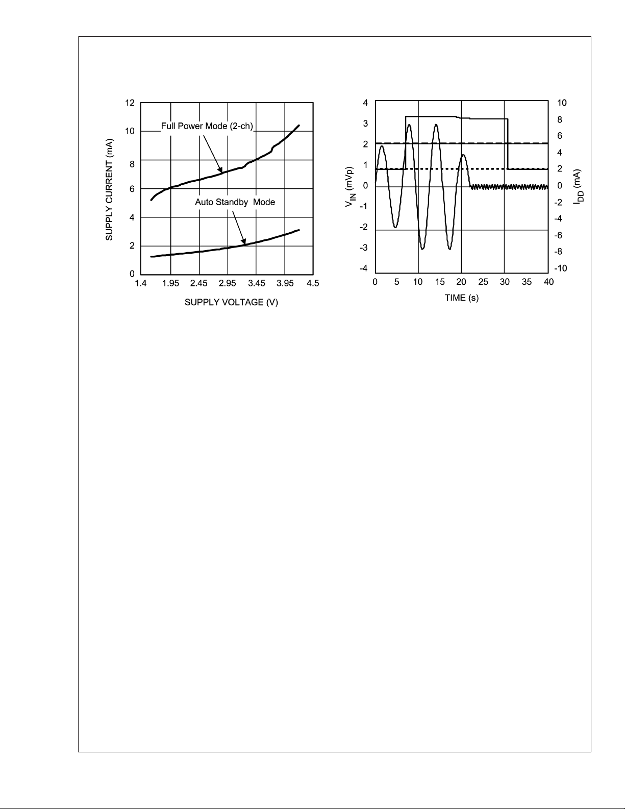
Supply Current vs Supply Voltage
R
=16Ω
L
20116189
Representation of Automatic Standby Mode Behavior
VDD=3V
20116119
www.national.com 16

Application Information
SUPPLY VOLTAGE SEQUENCING
It is a good general practice to first apply the supply voltage
to a CMOS device before any other signal or supply on other
pins. This is also true for the LM4926 audio amplifier which is
a CMOS device.
Before applying any signal to the inputs or shutdown pins of
the LM4926, it is important to apply a supply voltage to the
pins. After the device has been powered, signals may
V
DD
be applied to the shutdown pins (see MICRO POWER
SHUTDOWN) and input pins.
ELIMINATING THE OUTPUT COUPLING CAPACITOR
The LM4926 features a low noise inverting charge pump that
generates an internal negative supply voltage. This allows
the outputs of the LM4926 to be biased about GND instead
of a nominal DC voltage, like traditional headphone amplifiers. Because there is no DC component, the large DC
blocking capacitors (typically 220µF) are not necessary. The
coupling capacitors are replaced by two, small ceramic
charge pump capacitors, saving board space and cost.
Eliminating the output coupling capacitors also improves low
frequency response. In traditional headphone amplifiers, the
headphone impedance and the output capacitor form a high
pass filter that not only blocks the DC component of the
output, but also attenuates low frequencies, impacting the
bass response. Because the LM4926 does not require the
output coupling capacitors, the low frequency response of
the device is not degraded by external components.
In addition to eliminating the output coupling capacitors, the
ground referenced output nearly doubles the available dynamic range of the LM4926 when compared to a traditional
headphone amplifier operating from the same supply voltage.
OUTPUT TRANSIENT (’CLICK AND POPS’)
ELIMINATED
The LM4926 contains advanced circuitry that virtually eliminates output transients (’clicks and pops’). This circuitry
prevents all traces of transients when the supply voltage is
first applied or when the part resumes operation after coming
out of shutdown mode.
AMPLIFIER CONFIGURATION EXPLANATION
As shown in Figure 2, the LM4926 has two internal operational amplifiers. The two amplifiers have internally configured gain, the closed loop gain is set by selecting the ratio of
to Ri. Consequently, the gain for each channel of the IC is
R
f
POWER DISSIPATION
Power dissipation is a major concern when using any power
amplifier and must be thoroughly understood to ensure a
successful design. Equation 1 states the maximum power
dissipation point for a single-ended amplifier operating at a
given supply voltage and driving a specified output load.
P
=(VDD)2/(2π2RL) (1)
DMAX
Since the LM4926 has two operational amplifiers in one
package, the maximum internal power dissipation point is
twice that of the number which results from Equation 1. Even
with large internal power dissipation, the LM4926 does not
require heat sinking over a large range of ambient temperatures. From Equation 1, assuming a 3V power supply and a
16Ω load, the maximum power dissipation point is 28mW per
amplifier. Thus the maximum package dissipation point is
56mW. The maximum power dissipation point obtained must
not be greater than the power dissipation that results from
Equation 2:
=(T
P
DMAX
JMAX-TA
For the micro SMD package, θ
)/(θJA) (2)
= 105˚C/W. T
JA
JMAX
= 150˚C
for the LM4926. Depending on the ambient temperature, T
of the system surroundings, Equation 2 can be used to find
the maximum internal power dissipation supported by the IC
packaging. If the result of Equation 1 is greater than that of
Equation 2, then either the supply voltage must be decreased, the load impedance increased or T
reduced. For
A
the typical application of a 3V power supply, with a 16Ω load,
the maximum ambient temperature possible without violating
the maximum junction temperature is approximately 144˚C
provided that device operation is around the maximum
power dissipation point. Power dissipation is a function of
output power and thus, if typical operation is not around the
maximum power dissipation point, the ambient temperature
may be increased accordingly.
POWER SUPPLY BYPASSING
As with any power amplifier, proper supply bypassing is
critical for low noise performance and high power supply
rejection. Applications that employ a 3V power supply typically use a 4.7µF capacitor in parallel with a 0.1µF ceramic
filter capacitor to stabilize the power supply’s output, reduce
noise on the supply line, and improve the supply’s transient
response. Keep the length of leads and traces that connect
capacitors between the LM4926’s power supply pin and
ground as short as possible.
A
LM4926
,
AV= -(Rf/Ri) = 1.5 V/V
where R
= 30kΩ and Ri= 20kΩ.
F
Since this is an output ground-referenced amplifier, by driving the headphone through R
(Pin C2) and L
OUT
OUT
(Pin
D2), the LM4926 does not require output coupling capacitors. The typical single-ended amplifier configuration requires large, expensive output capacitors.
AUTOMATIC STANDBY MODE
The LM4926 features Automatic Standby Mode circuitry
(patent pending). In the absence of an input signal, after
approximately 12 seconds, the LM4926 goes into low current standby mode. The LM4926 recovers into full power
operating mode immediately after a signal, which is greater
than the input threshold voltage, is applied to either the left or
right input pins. The input threshold voltage is not a static
value, as the supply voltage increases, the input threshold
voltage decreases. This feature reduces power supply current consumption in battery operated applications. Please
see also the graph entitled Representation of Automatic
Standby Mode Behavior in the Typical Performance Characteristics section.
www.national.com17

Application Information (Continued)
To ensure correct operation of Automatic Standby Mode,
LM4926
proper layout techniques should be implemented. Separating PGND and SGND can help reduce noise entering the
LM4926 in noisy environments. Auto Standby mode works
best when output impedance of the audio source driving
LM4926 is equal or less than 50 Ohms. While Automatic
Standby Mode reduces power consumption very effectively
during silent periods, maximum power saving is achieved by
putting the device into shutdown when it is not in use.
MICRO POWER SHUTDOWN
The voltage applied to the SD_LC (shutdown left channel)
pin and the SD_RC (shutdown right channel) pin controls the
LM4926’s shutdown function. When active, the LM4926’s
micropower shutdown feature turns off the amplifiers’ bias
circuitry, reducing the supply current. The trigger point is
0.3*CPV
high level. The low 0.01µA (typ) shutdown current is
achieved by applying a voltage that is as near as ground a
possible to the SD_LC/SD_RC pins. A voltage that is higher
than ground may increase the shutdown current.
There are a few ways to control the micro-power shutdown.
These include using a single-pole, single-throw switch, a
microprocessor, or a microcontroller. When using a switch,
connect an external 100kΩ pull-up resistor between the
SD_LC/SD_RC pins and V
the SD_LC/SD_RC pins and ground. Select normal amplifier
operation by opening the switch. Closing the switch connects the SD_LC/SD_RC pins to ground, activating micropower shutdown. The switch and resistor guarantee that the
SD_LC/SD_RC pins will not float. This prevents unwanted
state changes. In a system with a microprocessor or microcontroller, use a digital output to apply the control voltage to
the SD_LC/SD_RC pins. Driving the SD_LC/SD_RC pins
with active circuitry eliminates the pull-up resistor.
SELECTING PROPER EXTERNAL COMPONENTS
Optimizing the LM4926’s performance requires properly selecting external components. Though the LM4926 operates
well when using external components with wide tolerances,
best performance is achieved by optimizing component values.
Charge Pump Capacitor Selection
Use low ESR (equivalent series resistance) (
ramic capacitors with an X7R dielectric for best performance. Low ESR capacitors keep the charge pump output
impedance to a minimum, extending the headroom on the
for a logic-low level, and 0.7*CPVDDfor logic-
DD
. Connect the switch between
DD
<
100mΩ) ce-
negative supply. Higher ESR capacitors result in reduced
output power from the audio amplifiers.
Charge pump load regulation and output impedance are
affected by the value of the flying capacitor (C1). A larger
valued C1 (up to 3.3uF) improves load regulation and minimizes charge pump output resistance. Beyond 3.3uF, the
switch-on resistance dominates the output impedance for
capacitor values above 2.2uF.
The output ripple is affected by the value and ESR of the
output capacitor (C2). Larger capacitors reduce output ripple
on the negative power supply. Lower ESR capacitors minimize the output ripple and reduce the output impedance of
the charge pump.
The LM4926 charge pump design is optimized for 2.2uF, low
ESR, ceramic, flying, and output capacitors.
Input Capacitor Value Selection
Amplifying the lowest audio frequencies requires high value
input coupling capacitors (C
in Figure 1). A high value ca-
i
pacitor can be expensive and may compromise space efficiency in portable designs. In many cases, however, the
speakers used in portable systems, whether internal or external, have little ability to reproduce signals below 150Hz.
Applications using speakers with this limited frequency response reap little improvement by using high value input and
output capacitors.
Besides affecting system cost and size, C
has an effect on
i
the LM4926’s click and pop performance. The magnitude of
the pop is directly proportional to the input capacitor’s size.
Thus, pops can be minimized by selecting an input capacitor
value that is no higher than necessary to meet the desired
−3dB frequency.
As shown in Figure 1, the internal input resistor, R
input capacitor, C
, produce a -3dB high pass filter cutoff
i
and the
i
frequency that is found using Equation (3). Conventional
headphone amplifiers require output capacitors; Equation (3)
can be used, along with the value of R
, to determine to-
L
wards the value of output capacitor needed to produce a
–3dB high pass filter cutoff frequency.
f
i-3dB
=1/2πRiC
i
(3)
Also, careful consideration must be taken in selecting a
certain type of capacitor to be used in the system. Different
types of capacitors (tantalum, electrolytic, ceramic) have
unique performance characteristics and may affect overall
system performance. (See the section entitled Charge Pump
Capacitor Selection.)
www.national.com 18

Application Information (Continued)
LM4926 micro SMD DEMO BOARD ARTWORK
Top Overlay Top Layer
LM4926
20116117
Mid Layer 1 Mid Layer 2
201161H1 201161H0
20116116
www.national.com19

Application Information (Continued)
LM4926
Bottom Layer
20116115
www.national.com 20

Revision History
Rev Date Description
1.0 6/22/05 Initial WEB release.
1.1 6/24/05 Added Mid Layer 1 and Mid Layer 2 boards, then re-released D/S to the WEB (per Nisha P.)
LM4926
www.national.com21

Physical Dimensions inches (millimeters) unless otherwise noted
14 – Bump micro SMD
Order Number LM4926TL
NS Package Number TLE1411A
±
X1 = 1.970
0.03mm, X2 = 1.970±0.03mm, X3 = 0.600±0.075mm,
National does not assume any responsibility for use of any circuitry described, no circuit patent licenses are implied and National reserves
the right at any time without notice to change said circuitry and specifications.
For the most current product information visit us at www.national.com.
LIFE SUPPORT POLICY
NATIONAL’S PRODUCTS ARE NOT AUTHORIZED FOR USE AS CRITICAL COMPONENTS IN LIFE SUPPORT DEVICES OR SYSTEMS
WITHOUT THE EXPRESS WRITTEN APPROVAL OF THE PRESIDENT AND GENERAL COUNSEL OF NATIONAL SEMICONDUCTOR
CORPORATION. As used herein:
1. Life support devices or systems are devices or systems
which, (a) are intended for surgical implant into the body, or
(b) support or sustain life, and whose failure to perform when
properly used in accordance with instructions for use
2. A critical component is any component of a life support
device or system whose failure to perform can be reasonably
expected to cause the failure of the life support device or
system, or to affect its safety or effectiveness.
provided in the labeling, can be reasonably expected to result
in a significant injury to the user.
BANNED SUBSTANCE COMPLIANCE
National Semiconductor manufactures products and uses packing materials that meet the provisions of the Customer Products
Stewardship Specification (CSP-9-111C2) and the Banned Substances and Materials of Interest Specification (CSP-9-111S2) and contain
no ‘‘Banned Substances’’ as defined in CSP-9-111S2.
Leadfree products are RoHS compliant.
National Semiconductor
Americas Customer
LM4926 Ground-Referenced, Ultra Low Noise, Fixed Gain, 80mW Stereo Headphone Amplifier
Support Center
Email: new.feedback@nsc.com
Tel: 1-800-272-9959
www.national.com
National Semiconductor
Europe Customer Support Center
Fax: +49 (0) 180-530 85 86
Email: europe.support@nsc.com
Deutsch Tel: +49 (0) 69 9508 6208
English Tel: +44 (0) 870 24 0 2171
Français Tel: +33 (0) 1 41 91 8790
National Semiconductor
Asia Pacific Customer
Support Center
Email: ap.support@nsc.com
National Semiconductor
Japan Customer Support Center
Fax: 81-3-5639-7507
Email: jpn.feedback@nsc.com
Tel: 81-3-5639-7560
 Loading...