

Page 1

LM4921
Low Voltage I2S 16-Bit Stereo DAC with Stereo
Headphone Power Amplifiers and Volume Control
January 2004
LM4921 Low Voltage I
Control
General Description
The LM4921 combines a 16-bit resolution stereo I2S input
digital-to-analog converter (DAC) with a stereo headphone
audio power amplifier. It is primarily designed for demanding
applications in mobile phones and other portable communication device applications. The LM4921 features an I
serial interface for the digital audio information and a 16-bit
SPI serial interface for internal register control and communication. With AV
single-ended load to a 26mW
(THD+N) of the LM4921 will be less than 0.5%. The LM4921
also features a programmable 32-step digital volume control
accessed through an SPI interface.
Boomer audio power amplifiers were designed specifically to
provide high quality output power with a minimal amount of
external components. It is, therefore, ideally suited for mobile phone and other low voltage applications where minimal
power consumption is a primary requirement.
The LM4921 features a low-power consumption shutdown
mode, and also has an internal thermal shutdown protection
mechanism.
and DVDD= 3.0VDCand driving a 32Ω
DD
output level the distortion
RMS
2
Key Specifications
j
PSRR at 217Hz, A/DVDD= 3V, (Fig. 1) 52dB (typ)
j
P
at AVDD= 3.0V, 32Ω
OUT
<
0.05% THD 13mW (typ)
S
<
0.5% THD 26mW (typ)
j
Supply voltage range
DV
DD
AV
(Note 8) 2.6V to 5.5V
DD
j
Shutdown current 1µA (typ)
Features
n 16-bit resolution stereo DAC
2
n I
S digital audio data serial interface
n SPI serial interface (control register)
n Volume Control (32 steps; 1.5 dB increments)
n Up to 50mW/channel stereo headphone amplifier
n Zero Crossing Detection for Silent Attenuation Steps
n 2.6V
n 2.6V
n Unity-gain stable headphone amplifiers
n Available in the 20-bump microSMD package
to 5.0VDCdigital supply voltage range
DC
to 5.5VDCanalog supply voltage range (Note 8)
DC
Applications
n Mobile phones
n PDAs
n Portable electronic devices
2.6V to 5.0V
2
S 16-Bit Stereo DAC with Stereo Headphone Power Amplifiers and Volume
Boomer®is a registered trademark of National Semiconductor Corporation.
© 2004 National Semiconductor Corporation DS200486 www.national.com
Page 2

Typical Application
LM4921
FIGURE 1. Typical Audio Amplifier Application Circuit
200486F6
www.national.com 2
Page 3

Connection Diagrams
LM4921
LM4921 Pin Configuration
Top View
20-Bump micro SMD
Order Number LM4921ITL, LM4921ITLX
See NS Package Number TLA20JKA
NC - No Connection
20-Bump micro SMD Marking
200486F9
X - Date Code
T - Die Traceability
G - Boomer Family
B9 - LM4921ITL
200486F8
www.national.com3
Page 4

LM4921 I/O Pin Descriptions
LM4921
PIN # (ITL) PIN NAME PIN TYPE
B1 I2S_CLK I/O I2S Clock
C2 I2S_DATA I I2S data
B2 I2S_WS I/O I2S L/R word select
E3 SPI_CLK I SPI clcock
E4 SPI_DATA I SPI data
D3 SPI_ENABLE I SPI Enable
E2 MCLK/XTAL_IN I Master Clock / Xtal input
D2 XTAL_OUT O Xtal output
C4 BYPASS I/O Analog VDD/2 bypass capacitor connection
B4 AV
DD
A3 AGND P Analog Ground
C1 DV
DD
A1 GNDD P Digital ground
D1 VDDX P XTAL Oscillator circuit supply
E1 GNDX P XTAL Oscillator circuit ground
B3 HP_L O HP left output
A4 HP_R O HP right output
A2 No Connect O Must let float
C3 No Connect NC NC
D4 No Connect NC NC
PIN DESCRIPTION
Input-I, Output-O,
Power-P, No Connect-NC
point
P Analog supply
P Digital Supply
www.national.com 4
Page 5
LM4921
Absolute Maximum Ratings (Notes 1, 2)
If Military/Aerospace specified devices are required,
please contact the National Semiconductor Sales Office/
Distributors for availability and specifications.
Supply Voltage 6.0V
Junction Temperature 150˚C
Thermal Resistance
θ
JA
Operating Ratings
Storage Temperature −65˚C to +150˚C
Input Voltage -0.3V to V
DD
+ 0.3V
Power Dissipation (Note 3) Internally Limited
ESD Susceptibility
Human body model (Note 4) 2000V
Machine model (Note 5) 200V
Temperature Range
T
≤ TA≤ T
MIN
MAX
Supply Voltage
DV
DD
AV
DD
−40˚C ≤ TA≤ 85˚C
2.6V ≤ DVDD≤ 5.0V
2.6V ≤ AVDD≤ 5.5V
Electrical Characteristics DVDD= 3.0V, AVDD= 5.0V, RL=32Ω (Notes 1, 2)
The following specifications apply for the circuit shown in Figure 1 unless otherwise specified. Limits apply for T
LM4921
Symbol Parameter Conditions
DV
AV
DI
DD
DD
DD
Digital Power Supply Voltage Note 8 3.0 V
Analog Power Supply Voltage Note 8 5.0 V
Digital Power Supply Quiescent
R
Load
=∞,f
= 11.2896MHz 3.5 7.5 mA (max)
MLCK
Current
AI
DD
Analog Power Supply Quiescent
R
Load
=∞,f
= 0MHz 6 10 mA (max)
MCLK
Current
I
SD
Total Shutdown Power Supply
Current
I
SB
Standby Current Analog and Digital together
SHUTDOWN SPI bits1&2setto
logic 0,
SPI, M
and I2S inputs at GND
CLK
All clocks off
V
FS
THD+N Total Harmonic Distortion + Noise fIN= 1kHz, P
Full-Scale Output Voltage Gain set at max 3.5 V
= 12mW
OUT
(Vol Control = 11111, I
to get 12mW at output)
P
O
PSRR Power Supply Rejection Ratio
SNR Signal-to-Noise Ratio f
DR Dynamic Range f
Headphone Amplifier Output Power THD = (0.5%), f
AV
DDCBYPASS
V
A-weighted-f
= 200mV
RIPPLE
= 1kHz sinewave at -60dBFS,
IN
CONV
= 1kHz sinewave at -60dBFS,
IN
OUT
= 2.0µF
P-P
= 44.1kHz
A-weighted
∆A
X
CH-CH
TALK
Channel-to-Channel Gain Mismatch fIN= 1kHz 0.06 dB
Channel-to-Channel Crosstalk f
= 44.1kHz,
CONV
= 1kHz sinewave at -3dB
f
IN
Volume Control Range Minimum Attenuation
Maximum Attenuation
Volume Control Control Step Size 1.5 dB
Mute Attenuation -102 dB
2
S input adj
= 1kHz 50 40 mW (min)
217Hz
FS
Typical Limit
(Note 6) (Notes 7, 9)
1 5 uA(max)
25 uA
0.03 %
62 45 dB (min)
82 dB
84 dB
72 dB
+3.0
-43.5
= 25˚C.
A
60˚C/W
Units
(Limits)
P-P
dB
dB
www.national.com5
Page 6

Electrical Characteristics DVDD= 3.0V, AVDD= 3.0V, RL=32Ω (Notes 1, 2)
The following specifications apply for the circuit shown in Figure 1 unless otherwise specified. Limits apply for T
LM4921
LM4921
Symbol Parameter Conditions
DV
AV
DI
DD
DD
DD
Digital Power Supply Voltage Note 8 3.0 V
Analog Power Supply Voltage Note 8 3.0 V
Digital Power Supply Quiescent
R
Load
=∞,f
= 11.2896MHz 3.5 7.5 mA (max)
MLCK
Current
AI
DD
Analog Power Supply Quiescent
R
Load
=∞,f
= 0MHz 5 9.0 mA (max)
MCLK
Current
I
SD
Total Shutdown Power Supply
Current
I
SB
Standby Current Analog and Digital together
SHUTDOWN SPI bits1&2setto
logic 0,
SPI, M
and I2S inputs at GND
CLK
All clocks off
V
FS
THD+N Total Harmonic Distortion + Noise fIN= 1kHz, P
Full-Scale Output Voltage Gain set at max 2.6 V
= 12mW
OUT
(Vol Cont = 11011, I
get 12mW at output)
P
O
PSRR Power Supply Rejection Ratio
SNR Signal-to-Noise Ratio f
DR Dynamic Range f
Headphone Amplifier Output Power THD = (0.5%), f
AV
DDCBYPASS
V
A-weighted-f
= 200mV
RIPPLE
= 1kHz sinewave at -60dBFS,
IN
CONV
= 1kHz sinewave at -60dBFS,
IN
OUT
= 2.0µF
P-P
= 44.1kHz
A-weighted
∆A
X
CH-CH
TALK
Channel-to-Channel Gain Mismatch fIN= 1kHz 0.06 dB
Channel-to-Channel Crosstalk f
= 44.1kHz,
CONV
= 1kHz sinewave at -3dB
f
IN
Volume Control Range Minimum Attenuation
Maximum Attenuation
Volume Control Control Step Size 1.5 dB
Mute Attenuation -100 dB
2
S input adj to
= 1kHz 26 mW (min)
217Hz
FS
Typical Limit
(Note 6) (Notes 7, 9)
1 uA(max)
15 uA
0.05 %
52 dB (min)
79 dB
81 dB
72 dB
0
-43.5
= 25˚C.
A
Units
(Limits)
P-P
dB
dB
www.national.com 6
Page 7

Electrical Characteristics-Digital Inputs DVDD= 3.0V (Notes 1, 2)
The following specifications apply for the circuit shown in Figure 1 unless otherwise specified. Limits apply for T
= 25˚C.
A
LM4921
Symbol Parameter Conditions
LM4921
Typical Limit
(Note 6) (Notes 7, 9)
Units
(Limits)
Resolution 16 Bits
2
I
S Audio Data Interface Format Standard, I2S, Left Justified
f
MCLK
Master Clock Frequency 11.2896
MHz
(256FS)
f
CONV
V
IL
Sampling Clock Frequency Range 44.1 48 kHz
Digital Input: Logic Low Voltage
0.3XDV
V (max)
DD
Level
V
IH
Digital Input: Logic High Voltage
0.7XDV
DD
V (min)
Level
t
ES
t
EH
t
EL
t
DS
t
DH
t
CS
t
CH
t
CL
f
CLK
t
CLKI
2
t
HII
2
t
LOI
t
SLRCLK
t
HLRCLK
2
t
SDI
t
HDI
Note 1: Absolute Maximum Ratings indicate limits beyond which damage to the device may occur. Operating Ratings indicate conditions for which the device is
functional, but do not guarantee specific performance limits. Electrical Characteristics state DC andAC electrical specifications under particular test conditions which
guarantee specific performance limits. This assumes that the device is within the Operating Ratings. Specifications are not guaranteed for parameters where no limit
is given, however, the typical value is a good indication of device performance.
Note 2: All voltages are measured with respect to the GND pin, unless otherwise specified.
Note 3: The maximum power dissipation must be derated at elevated temperatures and is dictated by T
allowable power dissipation is P
Note 4: Human body model, 100pF discharged through a 1.5kΩ resistor.
Note 5: Machine Model, 220pF – 240pF discharged through all pins.
Note 6: Typicals are measured at 25˚C and represent the parametric norm.
Note 7: Limits are guaranteed to National’s AOQL (Average Outgoing Quality Level).
Note 8: Best operation is achieved by maintaining 3.0V ≤ AV
Note 9: Datasheet min/max specification limits are guaranteed by design, test, or statistical analysis.
SPI_ENB Setup Time 20 ns (min)
SPI_ENB Hold Time 20 ns (min)
SPI_ENB Low Time 30 ns (min)
SPI_Data Setup Time 20 ns (min)
SPI_Data Hold Time 20 ns (min)
SPI_CLK Setup Time 20 ns (min)
SPI_CLK High Pulse Width 100 ns (min)
SPI_CLK Low Pulse Width 100 ns (min)
SPI_CLK Frequency 5 MHz (max)
2
SI2S_CLK Period 50 ns (min)
SI
S
2
S_CLK High Pulse Width 20 ns (min)
2
S_CLK Low Pulse Width 20 ns (min)
I
2
I
S_LRCLK Duty Cycle 50 %
I2S_LRCLK to I2S_CLK Setup Time 20 ns (min)
I2S_LRCLK to I2S_CLK Hold Time 20 ns (min)
SI2S_Data to I2S_CLK Setup Time 20 ns (min)
2
SI2S_Data to I2S_CLK Hold Time 20 ns (min)
, θJA, and the ambient temperature TA. The maximum
DMAX
=(T
)/θJAor the number given in Absolute Maximum Ratings, whichever is lower.
JMAX–TA
≤ 5.0V and 3.0V ≤ DVDD≤ 5.0V.
DD
JMAX
www.national.com7
Page 8

Typical Performance Characteristics
LM4921
THD+N vs Output Power THD+N vs Output Power
Analog VDD= 5V, Digital VDD=3V
200486G9
=32Ω, 44.1 kHz Sample Rate
R
L
R & L Channels, Vol = 3dB, Frequency in = 1kHz
THD+N vs Output Power THD+N vs Frequency
Analog VDD= 2.6V, Digital VDD= 2.6V
200486G7
=32Ω, 44.1 kHz Sample Rate
R
L
R & L Channels Shown, Vol = 3dB, Frequency in = 1kHz
THD+N vs Frequency THD+N vs Frequency
Analog VDD= 3V, Digital VDD=3V
200486G8
=32Ω, 44.1 kHz Sample Rate
R
L
R & L Channels Shown, Vol = 3dB, Frequency in = 1kHz
Analog VDD= 5V, Digital VDD=3V
200486G6
=32Ω, Power Level = 50mW
R
L
R & L Channels Shown, 44.1kHz Sample Rate
Analog VDD= 3V, Digital VDD=3V
200486G5
=32Ω, Power Level = 12mW
R
L
R & L Channels Shown, 44.1kHz Sample Rate
www.national.com 8
Analog VDD= 2.6V, Digital VDD= 2.6V
200486G4
=32Ω, Power Level = 12mW
R
L
R & L Channels Shown, 44.1kHz Sample Rate
Page 9
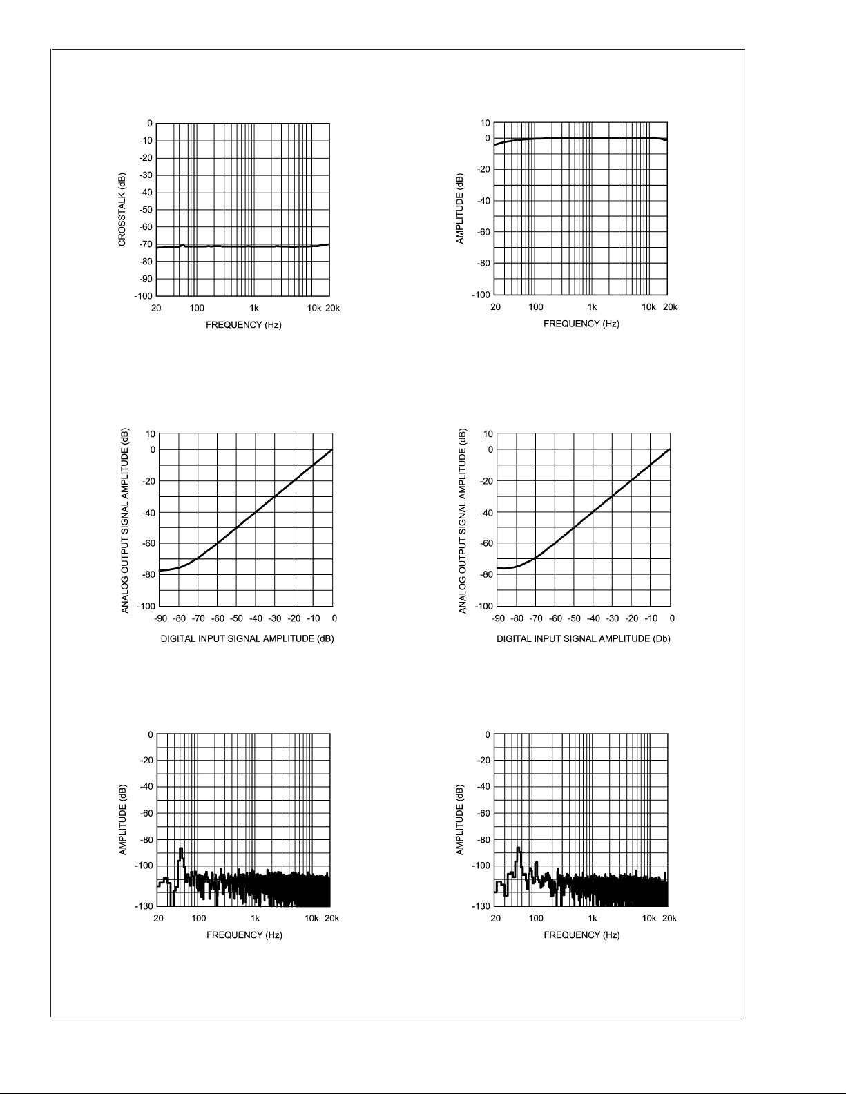
Typical Performance Characteristics (Continued)
Crosstalk Frequency Response
LM4921
Analog VDD= 3V, Digital VDD=3V
200486C7
RL=32Ω, Vol = 3dB
44.1kHz Sample Rate, -3dB FFS
Linearity Linearity
Analog VDD= 5V, Digital VDD=3V
200486E3
=32Ω, 44.1kHz Sample Rate
R
L
Noise Floor Noise Floor
Analog VDD= 5V, Digital VDD=3V
200486E1
RL=32Ω, Vol = 0dB
44.1kHz Sample Rate, 0dB FFS
Analog VDD= 3V, Digital VDD=3V
200486E2
=32Ω, 44.1kHz Sample Rate
R
L
Analog VDD= 5V, Digital VDD=3V
=32Ω, Vol = 3dB, 44.1kHz Sample Rate
R
L
200486F0
Analog VDD= 3V, Digital VDD=3V
=32Ω, Vol = 0dB, 44.1kHz Sample Rate
R
L
200486E9
www.national.com9
Page 10

Typical Performance Characteristics (Continued)
LM4921
PSRR vs Frequency PSRR vs Frequency
Analog VDD= 5V, Digital VDD=3V
=32Ω, Vol = 3dB, 44.1kHz Sample Rate
R
L
@
1kHz -60dB FFT@1kHz 0dB
FFT
200486G3
Analog VDD= 3V, Digital VDD=3V
=32Ω, Vol = 0dB, 44.1kHz Sample Rate
R
L
200486E7
Analog VDD= 5V, Digital VDD=3V
200486D1
=32Ω, Vol = 3dB, 44.1kHz Sample Rate
R
L
@
1kHz -60dB FFT@1kHz 0dB
FFT
200486D0
Analog VDD= 3V, Digital VDD=3V
=32Ω, Vol = 0dB, 44.1kHz Sample Rate
R
L
www.national.com 10
Analog VDD= 5V, Digital VDD=3V
=32Ω, Vol = 3dB, 44.1kHz Sample Rate
R
L
Analog VDD= 3V, Digital VDD=3V
=32Ω, Vol = 0dB, 44.1kHz Sample Rate
R
L
200486C9
200486F7
Page 11

Application Information
SPI OPERATIONAL DESCRIPTION
The serial data bits are organized into a field which contains 16 bits of data defined by TABLE 1. Bits1&2determine the output
mode of the LM4921 as shown in TABLE 2. Bits 7 through 11 determine the volume level setting as illustrated by TABLE 3. Bit
12 sets the Bypass capacitor charging time.
Table 1. Bit Allocation
BIT # Default Val Function Description
0 (LSB) 0 RESET_B RESET_B = 0, Resets the DAC
Must be high for the part to run.
10
20
3 0 MASTER/SLAVE 0 = SLAVE, 1 = MASTER
4 0 RESOLUTION 0 = 16 bit,1=32bit
5 0 RESERVED Should always be set to ’1’
6 0 ZERO CROSSING SET 0 = ZXD ENABLE,1=ZXD
7 0 VOLUME CONTROL See Table3-Volume Control
80
90
10 0
11 0
12 0 BYP CHARGE RATE 0 = 1X,1=2X
13 0 RESERVED
14 0 RESERVED
15 (MSB) 0 RESERVED Should always be set to ’0’
MODE CONTROL See Table 2
DISABLE
Settings
LM4921
MODE CONTROL
Sets the modes as outlined in Table 2.
Table 2. Output Mode Selection (Bits1&2above)
Output Mode # BIT 2 BIT 1 MODE
000 SD
1 0 1 STANDBY
2 1 0 MUTE
3 1 1 ACTIVE
Shutdown turns off the part completely for maximum power savings. The Standby mode turns off the clock but still consumes
more power than the shutdown mode. However, coming out of standby mode allows the part to turn back on faster than from
shutdown. In Mute mode the clocks remain on which uses more power but allows faster recovery and the ability to supply clock
signals to other devices which is important when the part is used in master mode. Active mode turns the part on for normal
operation.
MASTER/SLAVE SELECT
Allows the part to act as a master and supply the clock for
the rest of the system or be a slave to the system clock.
RESOLUTION SET
Sets the resolution to be either 16 or 32 bits of stereo audio
information. For most applications this will be set at 16 bits.
ZERO CROSSING DETECT SET
This pin turns on the zero crossing detection circuit. With this
circuit enabled the part will not allow a volume step change,
or shutdown mode, or standby mode to occur until the audio
input signal passes through zero. This pin should be set to
on for most applications.
www.national.com11
Page 12

Application Information (Continued)
VOLUME CONTROL
LM4921
The internal Stereo Volume Control is set by changing bits 7 through 11 in the SPI interface, as shown in table 3 below. The zero
dB setting is for 3V VDD operation and the +3dB is for 5V VDD.
Table 3. Volume Control Settings
Gain (dB)
HP_L & HP_R
-43.5 0 0 0 0 0
-42.0 0 0 0 0 1
-40.5 0 0 0 1 0
-39.0 0 0 0 1 1
-37.5 0 0 1 0 0
-36.0 0 0 1 0 1
-34.5 0 0 1 1 0
-33.0 0 0 1 1 1
-31.5 0 1 0 0 0
-30.0 0 1 0 0 1
-28.5 0 1 0 1 0
-27.0 0 1 0 1 1
-25.5 0 1 1 0 0
-24.0 0 1 1 0 1
-22.5 0 1 1 1 0
-21.0 0 1 1 1 1
-19.5 1 0 0 0 0
-18.0 1 0 0 0 1
-16.5 1 0 0 1 0
-15.0 1 0 0 1 1
-13.5 1 0 1 0 0
-12.0 1 0 1 0 1
-10.5 1 0 1 1 0
-9.0 1 0 1 1 1
-7.5 1 1 0 0 0
-6.0 1 1 0 0 1
-4.5 1 1 0 1 0
-3.0 1 1 0 1 1
-1.5 1 1 1 0 0
0.0 1 1 1 0 1
1.5 1 1 1 1 0
3.0 1 1 1 1 1
Bit 11 Bit 10 Bit 9 Bit 8 Bit 7
BYPASS CHARGE RATE BIT 12
This control pin allows the user to change the Bypass Capacitor’s charge rate by a factor of two. Setting this bit at
zero will set the circuit to it’s normal 1x rate. Setting the bit to
High will double the charge rate and allow the part to turn on
faster with a slight degradation in turn on click/pop noise.
SPI CONTROL INTERFACE BUS (J1)
SPI DATA: This is the serial data pin.
SPI CLK: This is the clock input pin.
SPI ENABLE: This is the SPI enable pin.
www.national.com 12
BITS 5, 13,14, and 15
Bits 13, 14, and 15 are all reserve bits and must be set to
low/zero/ground.
Bit 5 must be set High.
Page 13

Application Information (Continued)
SPI TIMING DIAGRAM
LM4921
200486G1
SPI OPERATIONAL REQUIREMENTS
1. The maximum clock rate is 5MHz for the CLK pin.
2. CLK must remain logic-high for at least 100ns (tCH) after
the rising edge of CLK, and CLK must remain logic-low for at
least 100ns (t
) after the falling edge of CLK.
CL
3. Data bits are written to the DATA pin with the least
significant bit (LSB) first.
4. The serial data bits are sampled at the rising edge of CLK.
Any transition on DATA must occur at least 20ns (t
) before
DS
the rising edge of CLK. Also, any transition on DATA must
occur at least 20ns (t
) after the rising edge of CLK and
DH
stabilize before the next rising edge of CLK.
5. ENABLE should be logic-high only during serial data
transmission.
6. ENABLE must be logic-high at least 20ns (t
) before the
ES
first rising edge of CLK, and ENABLE has to remain logichigh at least 20ns (t
) after the sixteenth rising edge of
EH
CLK.
7. If ENABLE remains logic-low for more than 10ns before all
16 bits are transmitted then the data latch will be aborted.
8. If ENABLE is logic-high for more than 16 CLK pulses then
only the first 16 data bits will be latched and activated at
rising edge of sixteenth CLK.
9. ENABLE must remain logic-low for at least 30ns (t
).
EL
10. Coincidental rising or falling edges of CLK and ENABLE
are not allowed. If CLK is to be held logic-high after the data
transmission, the falling edge of CLK must occur at least
20ns (t
) before ENABLE transitions to logic-high for the
CS
next set of data.
audio DAC. This interface uses a three wire system of clock
(I2S_CLK), data (I2S_DATA), and word select (I2S_WS,
sometimes called Right/Left Select).
A bit clock (I2S_CLK) at 32 or 64 times the sample frequency
is established by the I2S system master and the word select
(I2S_WS) line is driven at a frequency equal to the sampling
rate of the audio data, in this case 48kHz. The word line is
registered to change on the negative edge of the bit clock.
The serial data (I2S_DATA) is sent MSB first, again registers
on the negative edge of the bit clock, delayed by 1 bit clock
cycle relative to the changing of the word line (typical I
2
format).
MCLK/XTAL_IN (S1 MCLK SEL - Fig 2)
This is the input for an external Master Clock. The jumper at
S1 must be removed (disconnecting the onboard crystal
from the circuit) when using an external Master Clock.
STEREO HEADPHONE OUTPUT JACK (J3 - Fig 2)
This is the stereo headphone output. Each channel is singleended, with 100uF DC output blocking capacitors mounted
on the demo board (C6 and C7). These capacitors are
necessary to block the 1/2 VDD DC bias and prevent it from
flowing through the headphone speakers (DC current will
destroy most audio speakers) while allowing the audio ac
signal to pass through. The jack features a typical stereo
headphone pinout.
S
I2S INTERFACE BUS (J2 - Fig 2)
The I2S standard provides a uni-directional serial interface
designed specifically for digital audio. For the LM4921, the
interface provides access to a 48kHz, 16 bit full-range stereo
www.national.com13
Page 14

Application Information (Continued)
LM4921ITL DEMO BOARD OPERATION
LM4921
The LM4921ITL demo board is a complete evaluation platform (Note 10), designed to give easy access to the control pins of the
part and comprise all the necessary external passive components. There are separate analog and digital supply connectors, SPI
interface bus (J1) for the control lines, I
external MCLK input (P1) for use in place of the crystal on the demoboard.
2
S interface bus (J2) for full-range digital audio, stereo headphone output (J3), and an
FIGURE 2. LM4921ITL Demo Board Schematic
Note 10: Parallel Port SPI Interface Card and control software available.
200486G2
www.national.com 14
Page 15

Application Information (Continued)
DEMO BOARD BILL OF MATERIALS
National Semiconductor Corporation Bill of Material
Analog Audio LM4921ITL20 Eval Board
Assembly Part Number: 980011973-100
Revision A
Item Part Number Part Description Qty Ref Designator
1 551011973-001 LM4921 Eval Board PCB etch
001
2 LM4921 ITL20 micro SMD 20
Bumps
3 Cer Cap 22pF 50V 10%, size
1206
4 Cer Cap 0.1pF 50V 10%, size
1206
5 Tant Cap 1µF 16V 10%, 3216 3 C3, C5, C8
6 Tant Cap 220µF 16V 10%,
7243
7 1 meg ohm 1 R1
8 Crystal 11.2896MHz 1 Y1
9 Phone Jack 3.5mm Stereo 1 J3
10 Jumper Header 1X2 2 P1, S1
11 Jumper Header 1X3 2 J1
12 Jumper Header 1X5 2 J2
13 PCB Banana Jack,
Black-Mouser 164-6218
14 PCB Banana Jack,
Red-Mouser 164-6219
LM4921
1
1U1
2 C1, C2
1C4
2 C6, C7
4 A GND, D GND, GND (2)
4 A VDD, D VDD, HP L, HP
R
www.national.com15
Page 16

Application Information (Continued)
DEMO BOARD ARTWORKS
LM4921
Silkscreen Layer
Mid Layer 1
200486F3
200486F2
Top Layer
200486F1
200486H1
Mid Layer 2
www.national.com 16
Page 17

Application Information (Continued)
LM4921
Bottom Layer
200486H0
www.national.com17
Page 18

Physical Dimensions inches (millimeters) unless otherwise noted
Control
20 Bump micro SMD
Order Number LM4921ITL, LM4921ITLX
NS Package Number TLA20JKA
±
X1 = 2.200
0.03mm X2 = 2.720±0.03mm X3 = 0.600±0.075mm
S 16-Bit Stereo DAC with Stereo Headphone Power Amplifiers and Volume
2
LM4921 Low Voltage I
LIFE SUPPORT POLICY
NATIONAL’S PRODUCTS ARE NOT AUTHORIZED FOR USE AS CRITICAL COMPONENTS IN LIFE SUPPORT
DEVICES OR SYSTEMS WITHOUT THE EXPRESS WRITTEN APPROVAL OF THE PRESIDENT AND GENERAL
COUNSEL OF NATIONAL SEMICONDUCTOR CORPORATION. As used herein:
1. Life support devices or systems are devices or
systems which, (a) are intended for surgical implant
into the body, or (b) support or sustain life, and
whose failure to perform when properly used in
accordance with instructions for use provided in the
2. A critical component is any component of a life
support device or system whose failure to perform
can be reasonably expected to cause the failure of
the life support device or system, or to affect its
safety or effectiveness.
labeling, can be reasonably expected to result in a
significant injury to the user.
BANNED SUBSTANCE COMPLIANCE
National Semiconductor certifies that the products and packing materials meet the provisions of the Customer Products
Stewardship Specification (CSP-9-111C2) and the Banned Substances and Materials of Interest Specification
(CSP-9-111S2) and contain no ‘‘Banned Substances’’ as defined in CSP-9-111S2.
National Semiconductor
Americas Customer
Support Center
Email: new.feedback@nsc.com
Tel: 1-800-272-9959
www.national.com
National does not assume any responsibility for use of any circuitry described, no circuit patent licenses are implied and National reserves the right at any time without notice to change said circuitry and specifications.
National Semiconductor
Europe Customer Support Center
Fax: +49 (0) 180-530 85 86
Email: europe.support@nsc.com
Deutsch Tel: +49 (0) 69 9508 6208
English Tel: +44 (0) 870 24 0 2171
Français Tel: +33 (0) 1 41 91 8790
National Semiconductor
Asia Pacific Customer
Support Center
Email: ap.support@nsc.com
National Semiconductor
Japan Customer Support Center
Fax: 81-3-5639-7507
Email: jpn.feedback@nsc.com
Tel: 81-3-5639-7560
 Loading...