


May 2004
LM4919
1.5V, Mono 85mW BTL Output, 14mW Stereo Headphone
Audio Amplifier
LM4919 1.5V, Mono 85mW BTL Output, 14mW Stereo Headphone Audio Amplifier
General Description
The unity gain stable LM4919 is both a mono-BTL audio
power amplifier and a Single Ended (SE) stereo headphone
amplifier. Operating on a single 1.5V supply, the mono BTL
mode delivers 85mW into an 8Ω load at 1% THD+N. In
Single Ended stereo headphone mode, the amplifier delivers
14mW per channel into a 16Ω load at 1% THD+N.
With the LM4919 packaged in the MM package, the customer benefits include low profile and small size. This package minimizes PCB area and maximizes output power.
The LM4919 features circuitry that reduces output transients
("clicks" and "pops") during device turn-on and turn-off, an
externally controlled, low-power consumption, active-low
shutdown mode, and thermal shutdown. Boomer audio
power amplifiers are designed specifically to use few external components and provide high quality output power in a
surface mount package.
Typical Application
Key Specifications
n Mono-BTL output power
n (R
n Stereo Headphone output power
n (R
n Micropower shutdown current 0.02µA (typ)
n Supply voltage operating range 0.9V
n PSRR 1kHz, V
=8Ω,VDD= 1.5V, THD+N = 1%) 85mW (typ)
L
=16Ω,VDD= 1.5V, THD+N = 1%) 14mW (typ)
L
<
<
V
= 1.5V, RL=16Ω 72dB (typ)
DD
DD
2.5V
Features
n Single-cell 0.9V to 2.5V battery operation
n BTL mode for mono speaker
n Single ended headphone operation with coupling
capacitors
n Unity-gain stable
n "Click and pop" suppression circuitry
n Active low micropower shutdown
n Low current, active-low mute mode
n Thermal shutdown protection circuitry
Applications
n Portable one-cell audio products
n Portable one-cell electronic devices
20082101
FIGURE 1. Block Diagram
Boomer®is a registered trademark of National Semiconductor Corporation.
© 2004 National Semiconductor Corporation DS200821 www.national.com
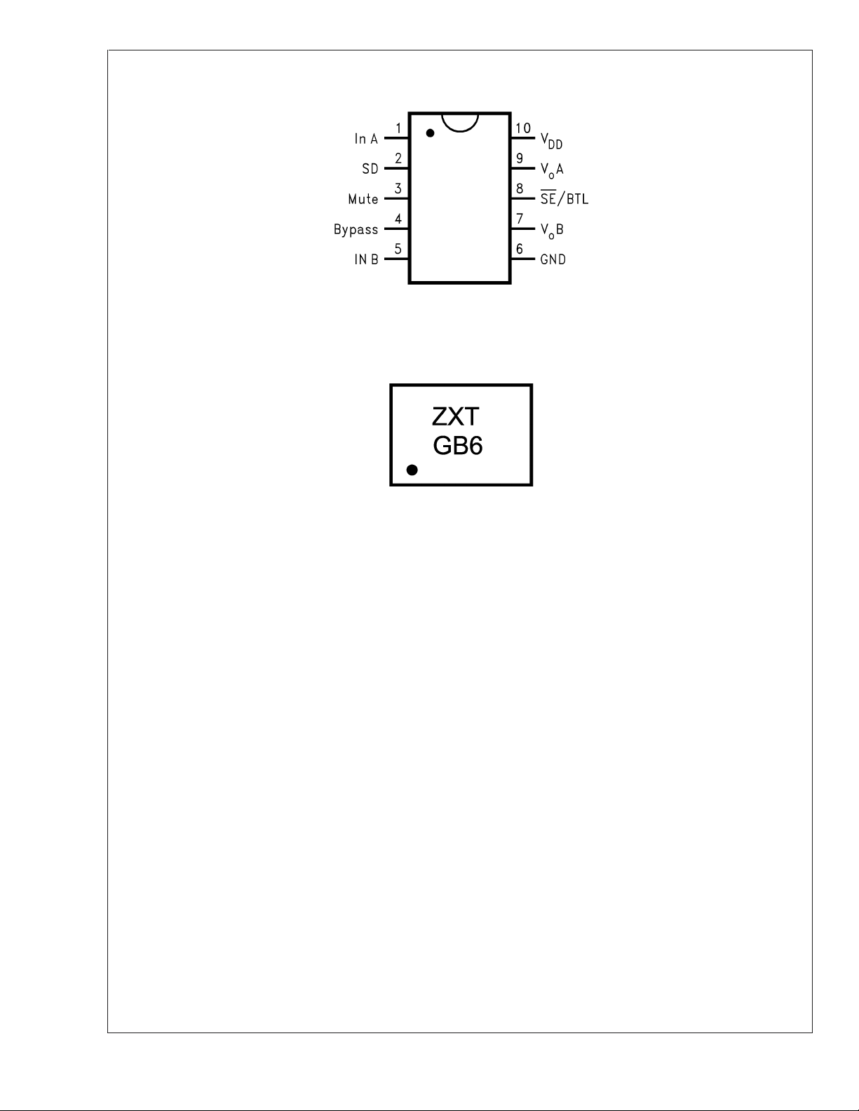
Connection Diagrams
LM4919
MSOP Package
Top View
20082102
Order Number LM4919MM
See NS Package Number MUB10A for MSOP
MSOP Marking
Z - Plant Code
200821F9
X - Date Code
T - Die Traceability
G - Boomer Family
B6 - LM4919MM
www.national.com 2
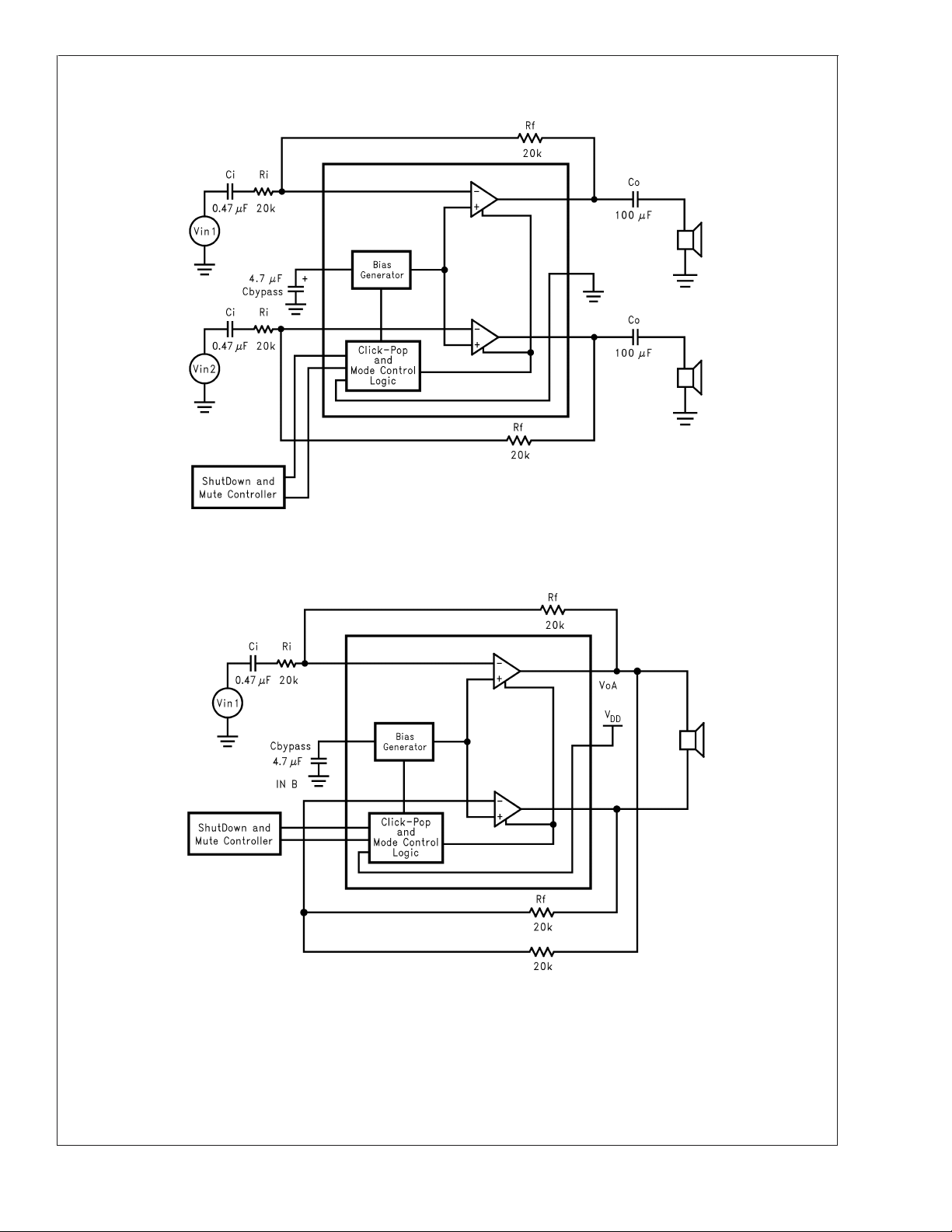
Typical Connections
LM4919
FIGURE 2. Typical Single Ended Output Configuration Circuit
20082103
FIGURE 3. Typical BTL Speaker Configuration Circuit
20082105
www.national.com3
Absolute Maximum Ratings (Note 1)
If Military/Aerospace specified devices are required,
LM4919
please contact the National Semiconductor Sales Office/
Distributors for availability and specifications.
Supply Voltage 3.6V
Junction Temperature 150˚C
Thermal Resistance
θ
(typ) MUB10A 175˚C/W
JA
Operating Ratings
Storage Temperature −65˚C to +150˚C
Input Voltage −0.3V to V
DD
+0.3V
Power Dissipation (Note 2) Internally limited
ESD Susceptibility(Note 3) 2000V
Temperature Range
T
MIN
≤ TA≤ T
MAX
−40˚C ≤ TA≤ 85˚C
Supply Voltage 0.9V ≤ V
ESD Susceptibility (Note 4) 200V
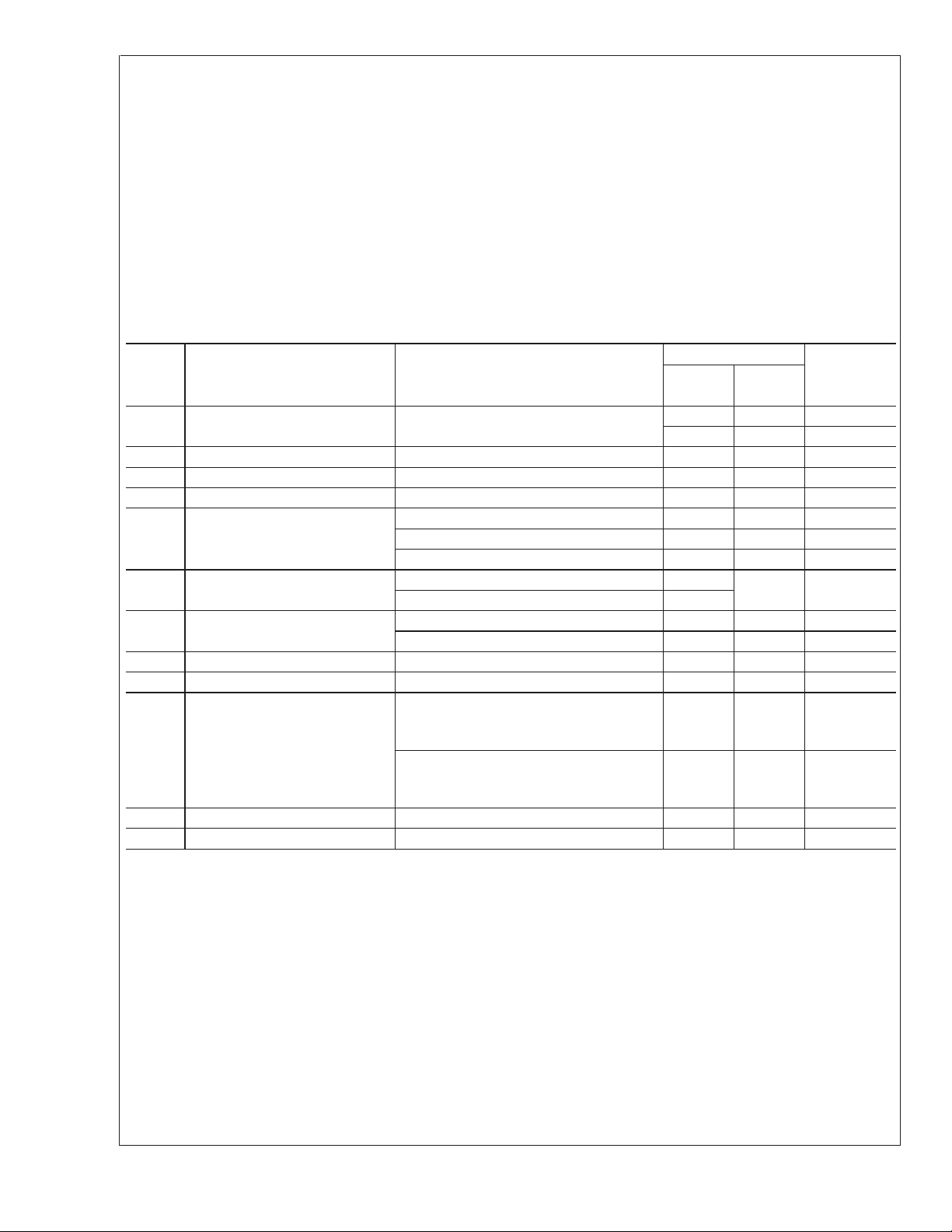
Electrical Characteristics for the LM4919 (Notes 1, 5)
The following specifications apply for the circuit shown in Figure 4 operating with VDD= 1. 5V, unless otherwise
DMAX
= 25˚C.
A
=(T
JMAX−TA
Typical Limit
(Note 6) (Note 7)
2.5 V (max)
SHUTDOWN
= GND 0.02 µA
f = 1kHz
RL=8Ω BTL, THD+N = 1% 85 70 mW (min)
R
=16Ω SE, THD+N = 1% 14 mW (min)
L
R
=8Ω, BTL, PO= 25mW, f = 1kHz 0.2
L
R
=16Ω, SE, PO= 5mW, f = 1kHz 0.07
L
0.5 % (max)
20Hz to 20kHz, A-weighted SE 10 µV
20Hz to 20kHz, A-weighted BTL 15 µV
=0,SE 15 µA
MUTE
=16Ω,SE 55 dB
L
V
C
RIPPLE
BYPASS
= 200mV
P-P
= 4.7µF, RL=8Ω
70 dB
f = 1kHz, BTL
V
C
= 200mV
RIPPLE
= 4.7µF, RL=16Ω
BYPASS
sine wave
P-P
72 dB
f = 1kHz, SE
, θJA, and the ambient temperature TAand must be derated at elevated temperatures. The maximum
JMAX
)/θJA. For the LM4919, T
= 150˚C. For the θJAs, please see the Application Information section or the
JMAX
specified. Limits apply for T
Symbol Parameter Conditions LM4919 Units
V
DD
I
DD
I
SD
V
OS
P
O
Supply Voltage (Notes 10, 11) 0.9 V (min)
Quiescent Power Supply Current VIN= 0V, IO= 0A, RL=∞(Note 8) 0.9 1.4 mA (max)
Shutdown Current V
Output Offset Voltage BTL 5 50 mV (max)
Output Power (Note 9)
THD+N Total Harmonic Distortion + Noise
V
I
MUTE
NO
Output Voltage Noise
Mute Current V
Crosstalk R
PSRR Power Supply Rejection Ratio
V
IH
V
IL
Control Logic High 0.9 V
Control Logic Low 0.3 V
Note 1: Absolute Maximum Ratings indicate limits beyond which damage to the device may occur. Operating Ratings indicate conditions for which the device is
functional, but do not guarantee specific performance limits. Electrical Characteristics state DC andAC electrical specifications under particular test conditions which
guarantee specific performance limits. This assumes that the device is within the Operating Ratings. Specifications are not guaranteed for parameters where no limit
is given, however, the typical value is a good indication of device performance.
Note 2: The maximum power dissipation is dictated by T
allowable power dissipation is P
Absolute Maximum Ratings section.
Note 3: Human body model, 100pF discharged through a 1.5kΩ resistor.
Note 4: Machine model, 220pF–240pF discharged through all pins.
Note 5: All voltages are measured with respect to the ground (GND) pins unless otherwise specified.
Note 6: Typicals are measured at 25˚C and represent the parametric norm.
Note 7: Datasheet min/max specification limits are guaranteed by design, test, or statistical analysis.
Note 8: The quiescent power supply current depends on the offset voltage when a practical load is connected to the amplifier.
Note 9: Output power is measured at the device terminals.
≤ 2.5V
DD
(Limits)
RMS
RMS
www.national.com 4
Typical Performance Characteristics
LM4919
THD+N vs Frequency
= 1.5V, PO= 5mW, RL=16Ω
V
DD
= –1, Single Ended Output
A
V
THD+N vs Frequency
= 1.2V, PO= 5mW
V
DD
=16Ω,AV= -1, Single Ended Output
R
L
THD+N vs Frequency
V
= 1.5V, RL=8Ω,PO= 25mW
DD
20082112 20082113
= -1, BTL Output
A
V
THD+N vs Frequency
V
= 1.2V, RL=8Ω,PO= 25mW
DD
= -1, BTL Output
A
V
THD+N vs Output Power
= 1.5V, RL=16Ω, f = 1kHz
V
DD
= -1, Single Ended Output
A
V
20082111 20082114
THD+N vs Output Power
V
= 1.5V, RL=8Ω, f = 1kHz
DD
= -1, BTL Output
A
V
20082117
20082115
www.national.com5

Typical Performance Characteristics (Continued)
LM4919
THD+N vs Output Power
V
= 1.2V, RL=16Ω, f = 1kHz
DD
= -1, Single Ended Output
A
V
20082118
Output Power vs Supply Voltage
f = 1kHz, R
= -1, Single Ended Output
A
V
=16Ω,
L
THD+N vs Output Power
V
= 1.2V, RL=8Ω, f = 1kHz
DD
= -1, BTL Output
A
V
20082116
Output Powe rvs Supply Voltage
f = 1kHz, R
= -1, BTL Output
A
V
=8Ω,
L
20082106
Output Power
vs Load Resistance
= 1.5V, f = 1kHz
V
DD
Single Ended Output, A
www.national.com 6
V
=-1
200821E5
Output Power
vs Load Resistance
V
= 1.5V, f = 1kHz
DD
BTL Output, A
V
=-1
20082107
200821E6

Typical Performance Characteristics (Continued)
LM4919
Output Power
vs Load Resistance
= 1.2V, RL=16Ω, f = 1kHz
V
DD
Single Ended Output, A
V
=-1
200821E3
Power Dissipation vs Output Power
f = 1kHz, A
V
=-1
Single Ended Output, Both Channels
Output Power
vs Load Resistance
V
= 1.2V, RL=8Ω, f = 1kHz
DD
BTL Output, A
V
=-1
200821E4
Power Dissipation vs Output Power
f = 1kHz, AV=-1
BTL Output
Channel Separation
=16Ω,PO= 5mW
R
L
Single Ended Output, A
20082124
Power Supply Rejection Ratio
V
V
=-1
= 1.5V, V
DD
RL=16Ω, Single Ended Output
RIPPLE
= 200mV
Input Terminated into 10Ω
20082110 20082121
20082123
PP
www.national.com7

Typical Performance Characteristics (Continued)
LM4919
Power Supply Rejection Ratio
V
DD
= 1.5V, V
RIPPLE
= 200mV
RL=8Ω, BTL Output
Input Terminated into 10Ω
Power Supply Rejection Ratio
V
DD
= 1.2V, V
RIPPLE
= 200mV
RL=8Ω, BTL Output
Input Terminated into 10Ω
Power Supply Rejection Ratio
= 1.2V, V
V
DD
PP
RL=16Ω, Single Ended Output
RIPPLE
= 200mV
PP
Input Terminated into 10Ω
20082120 20082122
Frequency Response
PP
vs Input Capacitor Size
VDD= 1.5V, RL=16Ω
<
AV = -1, BW
80kHz, Single Ended Output
20082119
Supply Voltage
vs Supply Current
200821F1
www.national.com 8
200821F8
Clipping Voltage
vs Supply Voltage
200821E2

Typical Performance Characteristics (Continued)
LM4919
Noise Floor
V
= 1.5V, RL=16Ω
DD
<
80kHz, Single Ended Output
BW
Shutdown Hysteresis Voltage
= 1.5V
V
DD
Noise Floor
V
= 1.5V, RL=8Ω
DD
<
80kHz, BTL Output
BW
20082109 20082108
Power Derating Curve
VDD= 1.5V
Mute Attenuation
vs Load Resistance
200821E1
200821F2
200821F4
Shutdown Current
Distribution
200821F7
www.national.com9

Application Information
LM4919
SINGLE ENDED (SE) CONFIGURATION EXPLANATION
As shown in Figure 2, the LM4919 has two operational
amplifiers internally, which have externally configurable gain.
The closed loop gain of the two configurable amplifiers is set
by selecting the ratio of Rf to Ri. Consequently, the gain for
each channel of the IC is
= -(Rf/Ri)
A
VD
amplifier is not current limited or clipped. In order to choose
an amplifier’s closed-loop gain without causing excessive
clipping, please refer to the Audio Power Amplifier Design
section.
A bridge configuration, such as the one used in LM4919,
also creates a second advantage over single-ended amplifiers. Since the differential outputs, Vo1 and Vo2, are biased
at half-supply, no net DC voltage exists across the load. This
eliminates the need for an output coupling capacitor which is
required in a single supply, single-ended amplifier configuration.
When the LM4919 operates in Single Ended mode, coupling
capacitors are used on each output (VoA and VoB) and the
SE/BTL pin (Pin 8) is connected to ground. These output
coupling capacitors blocks the half supply voltage to which
the output amplifiers are typically biased and couples the
audio signal to the headphones or other single-ended (SE)
loads. The signal return to circuit ground is through the
headphone jack’s sleeve.
BRIDGED (BTL) CONFIGURATION EXPLANATION
As shown in Figure 3, the LM4919 has two internal operational amplifiers. The first amplifier’s gain is externally configurable, while the second amplifier should be externally
fixed in a unity-gain, inverting configuration. The closed-loop
gain of the first amplifier is set by selecting the ratio of R
while the second amplifier’s gain should be fixed by the
R
i
f
two external 20kΩ resistors. Figure 3 shows that the output
of amplifier one serves as the input to amplifier two which
results in both amplifiers producing signals identical in magnitude, but out of phase by 180˚. Consequently, the differential gain for the IC is
= 2 *(Rf/Ri).
A
VD
By driving the load differentially through outputs Vo1 and
Vo2, an amplifier configuration commonly referred to as
"bridged mode" is established. Bridged mode operation is
different from the classical single-ended amplifier configuration where one side of the load is connected to ground. A
bridge amplifier design has a few distinct advantages over
the single-ended configuration. It provides a differential drive
to the load, thus doubling output swing for a specified supply
voltage. Four times the output power is possible as compared to a single-ended amplifier under the same conditions.
This increase in attainable output power assumes that the
MODE SELECT DETAIL
The LM4919 can be configured in either Single Ended or
BTL mode (see Figure 2 and Figure 3). The default state of
the LM4919 at power up is single ended. During initial power
up or return from shutdown, the LM4919 must detect the
correct mode of operation by sensing the status of the
SE/BTL pin. When the bias voltage of the part ramps up to
60mV (as seen on the Bypass pin), an internal comparator
detects the status of SE/BTL; and at 10mV, latches that
value in place. Ramp up of the bias voltage will proceed at a
different rate from this point on depending upon operating
mode. BTL mode will ramp up about 11 times faster than
Single Ended mode. Shutdown is not a valid command
during this time period (T
to
ensure a proper power on reset (POR) signal. In addition,
the slew rate of V
must be greater than 2.5V/ms to ensure
DD
) and should not enabled to
WU
reliable POR. Recommended power up timing is shown in
Figure 5 along with proper usage of Shutdown and Mute.
The mode-select circuit is suspended during C
discharge
B
time. The circuit shown in Figure 4 presents an applications
solution to the problem of using different supply voltages
with different turn-on times in a system with the LM4919.
This circuit shows the LM4919 with a 25-50kΩ. Pull-up resistor connected from the shutdown pin to V
. The shut-
DD
down pin of the LM4919 is also being driven by an open
drain output of an external microcontroller on a separate
supply. This circuit ensures that shutdown is disabled when
powering up the LM4919 by either allowing shutdown to be
high before the LM4919 powers on (the microcontroller powers up first) or allows shutdown to ramp up with V
(the
DD
LM4919 powers up first). This will ensure the LM4919 powers up properly and enters the correct mode of operation.
Please note that the SE/BTL pin (Pin 8) should be tied to
GND for Single Ended mode, and to VDDfor BTL mode.
www.national.com 10

Application Information (Continued)
LM4919
20082153
FIGURE 4. Recommended Circuit for Different Supply Turn-On Timing
FIGURE 5. Turn-On, Shutdown, and Mute Timing for Single-Ended
20082154
www.national.com11

Application Information (Continued)
POWER DISSIPATION
LM4919
Power dissipation is a major concern when designing a
successful amplifier, whether the amplifier is bridged or
single-ended. A direct consequence of the increased power
delivered to the load by a bridge amplifier is an increase in
internal power dissipation. Since the LM4919 has two operational amplifiers in one package, the maximum internal
power dissipation is 4 times that of a single-ended amplifier.
The maximum power dissipation for a given BTL application
can be derived from the power dissipation graphs or from
Equation 1.
= 4*(VDD)2/(2π2RL) (1)
P
DMAX
When operating in Single Ended mode, Equation 2 states
the maximum power dissipation point for a single-ended
amplifier operating at a given supply voltage and driving a
specified output load.
=(VDD)2/(2π2RL) (2)
P
DMAX
Since the LM4919 has two operational amplifiers in one
package, the maximum internal power dissipation point is
twice that of the number that results from Equation 2. From
Equation 2, assuming a 1.5V power supply and a 16Ω load,
the maximum power dissipation point is 7mW per amplifier.
Thus the maximum package dissipation point is 14mW.
The maximum power dissipation point obtained from either
Equations 1, 2 must not be greater than the power dissipation that results from Equation 3:
=(T
P
DMAX
For package MUB10A, θ
JMAX-TA
= 175˚C/W. T
JA
the LM4919. Depending on the ambient temperature, T
the system surroundings, Equation 3 can be used to find the
maximum internal power dissipation supported by the IC
packaging. If the result of Equation 1 or 2 is greater than that
of Equation 3, then either the supply voltage must be decreased, the load impedance increased or T
the typical application of a 1.5V power supply, with a 16Ω
load, the maximum ambient temperature possible without
violating the maximum junction temperature is approximately
146˚C provided that device operation is around the maximum power dissipation point. Thus, for typical applications,
power dissipation is not an issue. Power dissipation is a
function of output power and thus, if typical operation is not
around the maximum power dissipation point, the ambient
temperature may be increased accordingly. Refer to the
Typical Performance Characteristics curves for power dissipation information for lower output powers.
POWER SUPPLY BYPASSING
As with any amplifier, proper supply bypassing is important
for low noise performance and high power supply rejection.
The capacitor location on the power supply pins should be
as close to the device as possible. Typical applications employ a battery (or 1.5V regulator) with 10µF tantalum or
electrolytic capacitor and a ceramic bypass capacitor that
aid in supply stability. This does not eliminate the need for
bypassing the supply nodes of the LM4919. A bypass capacitor value in the range of 0.1µF to 1µF is recommended.
)/θ
JA
JMAX
A
(3)
= 150˚C for
,of
A
reduced. For
MICRO POWER SHUTDOWN
The voltage applied to the SHUTDOWN pin controls the
LM4919’s shutdown function. Activate micro-power shutdown by applying a logic-low voltage to the SHUTDOWN
pin. When active, the LM4919’s micro-power shutdown feature turns off the amplifier’s bias circuitry, reducing the supply current. The trigger point varies depending on supply
voltage and is shown in the Shutdown Hysteresis Voltage
graphs in the Typical Performance Characteristics section.
The low 0.02µA (typ) shutdown current is achieved by applying a voltage that is as near as ground as possible to the
SHUTDOWN pin. A voltage that is higher than ground may
increase the shutdown current. There are a few ways to
control the micro-power shutdown. These include using a
single-pole, single-throw switch, a microprocessor, or a microcontroller. When using a switch, connect an external
100kΩ pull-up resistor between the SHUTDOWN pin and
. Connect the switch between the SHUTDOWN pin and
V
DD
ground. Select normal amplifier operation by opening the
switch. Closing the switch connects the SHUTDOWN pin to
ground, activating micro-power shutdown. The switch and
resistor guarantee that the SHUTDOWN pin will not float.
This prevents unwanted state changes. In a system with a
microprocessor or microcontroller, use a digital output to
apply the control voltage to the SHUTDOWN pin. Driving the
SHUTDOWN pin with active circuitry eliminates the pull-up
resistor.
MUTE
When in single ended mode, the LM4919 also features a
mute function that enables extremely fast turn-on/turn-off
with a minimum of output pop and click with a low current
consumption (≤20µA, typical). The mute function leaves the
outputs at their bias level, thus resulting in higher power
consumption than shutdown mode, but also provides much
faster turn on/off times. Providing a logic low signal on the
MUTE pin enables mute mode. Threshold voltages and activation techniques match those given for the shutdown function as well. Mute may not appear to function when the
LM4919 is used to drive high impedance loads. This is
because the LM4919 relies on a typical headphone load
(16-32Ω) to reduce input signal feed-through through the
input and feedback resistors. Mute attenuation can thus be
calculated by the following formula:
Mute Attenuation (dB) = 20Log[R
/ (Ri+RF)]
L
Parallel load resistance may be necessary to achieve satisfactory mute levels when the application load is known to be
high impedance. The mute function, described above, is not
necessary when the LM4919 is operating in BTL mode since
the shutdown function operates quickly in BTL mode with
less power consumption than mute. In these modes, the
Mute signal is equivalent to the Shutdown signal. Mute may
be enabled during shutdown transitions, but should not be
toggled for a brief period immediately after exiting or entering
shutdown. These brief time periods are labeled X1 (time
after returning from shutdown) and X2 (time after entering
shutdown) and are shown in the timing diagram given in
Figure 5. X1 occurs immediately following a return from
±
shutdown (TWU) and lasts 40ms
25%. X2 occurs after the
part is placed in shutdown and the decay of the bias voltage
±
has occurred (2.2*250k*CB) and lasts for 100ms
25%. The
timing of these transition periods relative to X1 and X2 is also
shown in Figure 5. While in single ended mode, mute should
not be toggled during these time periods, but may be toggled
www.national.com 12

Application Information (Continued)
during the shutdown transitions or any other time the part is
in normal operation. Failure to operate mute correctly may
result in much higher click and pop values or failure of the
device to mute at all.
PROPER SELECTION OF EXTERNAL COMPONENTS
Proper selection of external components in applications using integrated power amplifiers is critical to optimize device
and system performance. While the LM4919 is tolerant of
external component combinations, consideration to component values must be used to maximize overall system quality. The LM4919 is unity-gain stable that gives the designer
maximum system flexibility. The LM4919 should be used in
low gain configurations to minimize THD+N values, and
maximize the signal to noise ratio. Low gain configurations
require large input signals to obtain a given output power.
Input signals equal to or greater than 1V
from sources such as audio codecs. Very large values
should not be used for the gain-setting resistors. Values for
and Rfshould be less than 1MΩ. Please refer to the
R
i
section, Audio Power Amplifier Design, for a more complete
explanation of proper gain selection. Besides gain, one of
the major considerations is the closed-loop bandwidth of the
amplifier. To a large extent, the bandwidth is dictated by the
choice of external components shown in Figures 2 and 3.
The input coupling capacitor, C
, forms a first order high pass
i
filter that limits low frequency response. This value should be
chosen based on needed frequency response and turn-on
time.
SELECTION OF INPUT CAPACITOR SIZE
Amplifying the lowest audio frequencies requires a high
value input coupling capacitor, C
. A high value capacitor can
i
be expensive and may compromise space efficiency in portable designs. In many cases, however, the headphones
used in portable systems have little ability to reproduce
signals below 60Hz.Applications using headphones with this
limited frequency response reap little improvement by using
a high value input capacitor. In addition to system cost and
size, turn on time is affected by the size of the input coupling
capacitor C
. A larger input coupling capacitor requires more
i
charge to reach its quiescent DC voltage. This charge
comes from the output via the feedback. Thus, by minimizing
the capacitor size based on necessary low frequency response, turn-on time can be minimized. A small value of C
(in the range of 0.1µF to 0.47µF), is recommended.
Bypass Capacitor Value Selection
Besides minimizing the input capacitor size, careful consideration should be paid to value of C
nected to the BYPASS pin. Since C
B
B
the LM4919 settles to quiescent operation, its value is critical
when minimizing turn-on pops. The slower the LM4919’s
outputs ramp to their quiescent DC voltage (nominally V
2), the smaller the turn-on pop. Choosing C
along with a small value of C
(in the range of 0.1µF to
i
0.47µF), produces a click-less and pop-less shutdown function. As discussed above, choosing C
no larger than neces-
i
sary for the desired bandwidth helps minimize clicks and
pops. This ensures that output transients are eliminated
when power is first applied or the LM4919 resumes operation after shutdown.
are available
rms
, the capacitor con-
determines how fast
equal to 4.7µF
B
DD
LM4919
OPTIMIZING CLICK AND POP REDUCTION PERFORMANCE
The LM4919 contains circuitry that eliminates turn-on and
shutdown transients ("clicks and pops"). For this discussion,
turn-on refers to either applying the power supply voltage or
when the micro-power shutdown mode is deactivated.
As the V
final value, the LM4919’s internal amplifiers are configured
as unity gain buffers. An internal current source charges the
capacitor connected between the BYPASS pin and GND in a
controlled, linear manner. Ideally, the input and outputs track
the voltage applied to the BYPASS pin. The gain of the
internal amplifiers remains unity until the voltage on the
bypass pin reaches V
bypass pin is stable, the device becomes fully operational
and the amplifier outputs are reconnected to their respective
output pins. Although the BYPASS pin current cannot be
modified, changing the size of C
time. There is a linear relationship between the size of C
and the turn-on time. Here are some typical turn-on times for
various values of C
In order to eliminate "clicks and pops", all capacitors must be
i
discharged before turn-on. Rapidly switching V
allow the capacitors to fully discharge, which may cause
"clicks and pops".
AUDIO POWER AMPLIFIER DESIGN
A 25mW/32Ω Audio Amplifier
Given:
/
Power Output 10mWrms
Load Impedance 16Ω
Input Level 0.4Vrms
Input Impedance 20kΩ
A designer must first choose a mode of operation (SE or
BTL) and determine the minimum supply rail to obtain the
specified output power. By extrapolating from the Output
Power vs. Supply Voltage graphs in the Typical Performance
Characteristics section, the supply rail can be easily found.
1.5V is a standard voltage in most applications, it is chosen
/2 voltage present at the BYPASS pin ramps to its
DD
/2. As soon as the voltage on the
DD
alters the device’s turn-on
B
:
B
Single-Ended
CB(µF) T
ON
0.1 117ms
0.22 179ms
0.47 310ms
1.0 552ms
2.2 1.14s
4.7 2.4s
BTL
CB(µF) TON(ms)
0.1 72
0.22 79
0.47 89
1.0 112
2.2 163
4.7 283
may not
DD
B
www.national.com13

Application Information (Continued)
for the supply rail. Extra supply voltage creates headroom
LM4919
that allows the LM4919 to reproduce peak in excess of
10mW without producing audible distortion. At this time, the
designer must make sure that the power supply choice along
with the output impedance does not violate the conditions
explained in the Power Dissipation section. Once the power
dissipation equations have been addressed, the required
gain can be determined from Equation 2.
From Equation 4, the minimum AV is 1; use A
desired input impedance is 20k, and with a A
ratio of 1:1 results from Equation 1 for R
are chosen with R
= 20k and Rf= 20k. The final design step
i
is to address the bandwidth requirements which must be
stated as a pair of -3dB frequency points. Five times away
V
to R. The values
f
(4)
= 1. Since the
gain of 1, a
V
from a -3dB point is 0.17dB down from passband response
±
which is better than the required
= 100Hz/5 = 20Hz
f
L
= 20kHz*5=100kHz
f
H
As stated in the External Components section, R
junction with C
creates a
i
0.25dB specified.
in con-
i
Ci≥ 1/(2π * 20kΩ * 20Hz) = 0.397µF; use 0.39µF.
The high frequency pole is determined by the product of the
desired frequency pole, fH, and the differential gain, A
= 1 and fH= 100kHz, the resulting GBWP = 100kHz
an AV
V
. With
V
which is much smaller than the LM4919 GBWP of 3MHz.
This example displays that if a designer has a need to design
an amplifier with higher differential gain, the LM4919 can still
be used without running into bandwidth limitations.
www.national.com 14

Physical Dimensions inches (millimeters)
unless otherwise noted
LM4919 1.5V, Mono 85mW BTL Output, 14mW Stereo Headphone Audio Amplifier
MSOP Package
Order Number LM4919MM
NS Package Number MUB10A
LIFE SUPPORT POLICY
NATIONAL’S PRODUCTS ARE NOT AUTHORIZED FOR USE AS CRITICAL COMPONENTS IN LIFE SUPPORT
DEVICES OR SYSTEMS WITHOUT THE EXPRESS WRITTEN APPROVAL OF THE PRESIDENT AND GENERAL
COUNSEL OF NATIONAL SEMICONDUCTOR CORPORATION. As used herein:
1. Life support devices or systems are devices or
systems which, (a) are intended for surgical implant
into the body, or (b) support or sustain life, and
whose failure to perform when properly used in
accordance with instructions for use provided in the
2. A critical component is any component of a life
support device or system whose failure to perform
can be reasonably expected to cause the failure of
the life support device or system, or to affect its
safety or effectiveness.
labeling, can be reasonably expected to result in a
significant injury to the user.
BANNED SUBSTANCE COMPLIANCE
National Semiconductor certifies that the products and packing materials meet the provisions of the Customer Products
Stewardship Specification (CSP-9-111C2) and the Banned Substances and Materials of Interest Specification
(CSP-9-111S2) and contain no ‘‘Banned Substances’’ as defined in CSP-9-111S2.
National Semiconductor
Americas Customer
Support Center
Email: new.feedback@nsc.com
Tel: 1-800-272-9959
www.national.com
National does not assume any responsibility for use of any circuitry described, no circuit patent licenses are implied and National reserves the right at any time without notice to change said circuitry and specifications.
National Semiconductor
Europe Customer Support Center
Fax: +49 (0) 180-530 85 86
Email: europe.support@nsc.com
Deutsch Tel: +49 (0) 69 9508 6208
English Tel: +44 (0) 870 24 0 2171
Français Tel: +33 (0) 1 41 91 8790
National Semiconductor
Asia Pacific Customer
Support Center
Email: ap.support@nsc.com
National Semiconductor
Japan Customer Support Center
Fax: 81-3-5639-7507
Email: jpn.feedback@nsc.com
Tel: 81-3-5639-7560
 Loading...