

Page 1
February 2004
LM4908
10kV ESD Rated, Dual 120 mW Headphone Amplifier
10kV ESD Rated, Dual 120 mW Headphone Amplifier
General Description
The LM4908 is a dual audio power amplifier capable of
delivering 120mW per channel of continuous average power
into a 16Ω load with 0.1% (THD+N) from a 5V power supply.
Boomer audio power amplifiers were designed specifically to
provide high quality output power with a minimal amount of
external components using surface mount packaging. Since
the LM4908 does not require bootstrap capacitors or snubber networks, it is optimally suited for low-power portable
systems.
The unity-gain stable LM4908 can be configured by external
gain-setting resistors.
Key Specifications
j
THD+N at 1kHz at 120mW
continuous average output power
into 16Ω 0.1% (typ)
j
THD+N at 1kHz at 75mW
continuous average output power
into 32Ω 0.1% (typ)
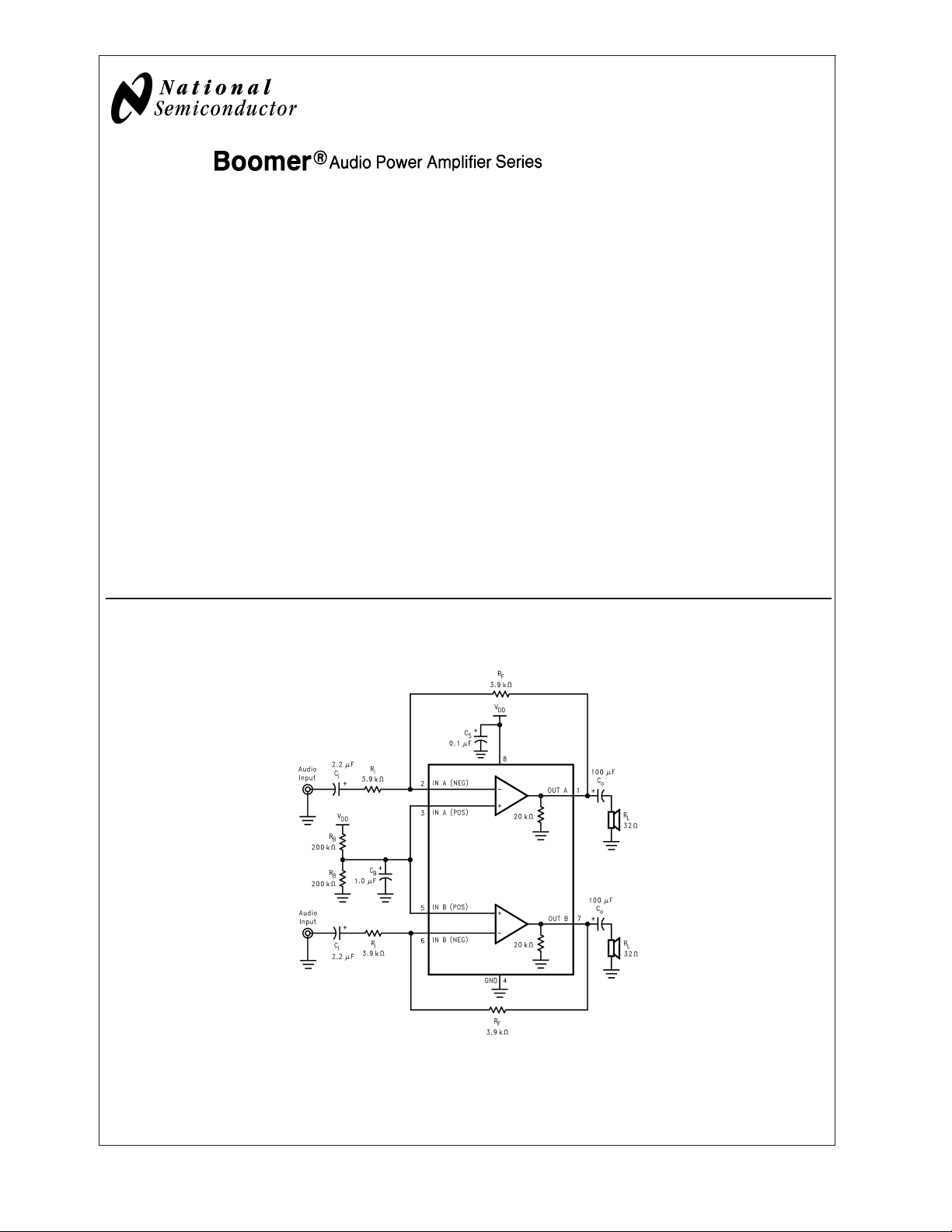
Typical Application
j
Output power at 0.1% THD+N
at 1kHz into 32Ω 75mW (typ)
Features
n Up to 10kV ESD protection on all pins
n MSOP, SOP, and LLP surface mount packaging
n Switch on/off click suppression
n Excellent power supply ripple rejection
n Unity-gain stable
n Minimum external components
Applications
n Headphone Amplifier
n Personal Computers
n Portable electronic devices
*Refer to the Application Information Section for information concerning proper selection of the input and output coupling capacitors.
FIGURE 1. Typical Audio Amplifier Application Circuit
Boomer®is a registered trademark of National Semiconductor Corporation.
© 2004 National Semiconductor Corporation DS200752 www.national.com
20075201
Page 2
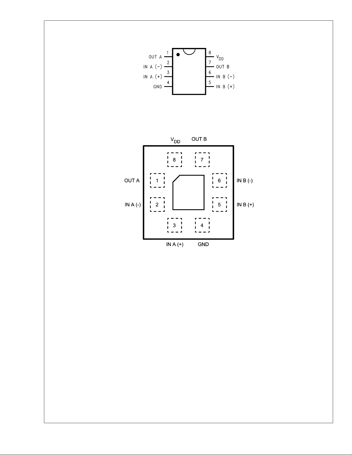
Connection Diagrams
LM4908
SOP (MA) and MSOP (MM) Package
Top View
20075202
Order Number LM4908MA, LM4908MM
See NS Package Number M08A, MUA08A
LLP (LQ) Package
Top View
Order Number LM4908LQ
See NS Package Number LQB08A
200752A2
www.national.com 2
Page 3
LM4908
Absolute Maximum Ratings (Note 3)
If Military/Aerospace specified devices are required,
please contact the National Semiconductor Sales Office/
Distributors for availability and specifications.
Supply Voltage 6.0V
Storage Temperature −65˚C to +150˚C
Input Voltage −0.3V to V
DD
+ 0.3V
θ
(MSOP) 56˚C/W
JC
θ
(MSOP) 210˚C/W
JA
θ
(SOP) 35˚C/W
JC
θ
(SOP) 170˚C/W
JA
θ
(LLP) 15˚C/W
JC
θ
(LLP) 117˚C/W (Note 9)
JA
θ
(LLP) 150˚C/W (Note 10)
JA
Power Dissipation (Note 4) Internally limited
ESD Susceptibility (Note 5) 10.0kV
Operating Ratings
ESD Susceptibility (Note 6) 500V
Junction Temperature 150˚C
Soldering Information (Note 1)
Small Outline Package
Vapor Phase (60 seconds) 215˚C
Infrared (15 seconds) 220˚C
Temperature Range
T
≤ TA≤ T
MIN
MAX
Supply Voltage 2.0V ≤ V
Note 1: See AN-450 “Surface Mounting and their Effects on Product Reliability” for other methods of soldering surface mount devices.
−40˚C ≤ TA≤ 85˚C
≤ 5.5V
DD
Thermal Resistance
Electrical Characteristics (Notes 2, 3)
The following specifications apply for VDD= 5V unless otherwise specified, limits apply to TA= 25˚C.
Symbol Parameter Conditions LM4908 Units
Typ
(Note 7)
V
DD
Supply Voltage 2.0 V (min)
Limit
(Note 8)
5.5 V (max)
I
DD
P
tot
V
OS
Supply Current VIN= 0V, IO= 0A 1.6 3.0 mA (max)
Total Power Dissipation VIN= 0V, IO= 0A 8 16.5 mW (max)
Input Offset Voltage VIN= 0V 5 50 mV (max)
Ibias Input Bias Current 10 pA
V
CM
G
V
Io Max Output Current THD+N
R
O
V
O
Common Mode Voltage
Open-Loop Voltage Gain RL=5kΩ 67 dB
<
0.1 % 70 mA
Output Resistance 0.1 Ω
Output Swing RL=32Ω, 0.1% THD+N, Min .3
R
=32Ω, 0.1% THD+N, Max 4.7
L
PSRR Power Supply Rejection Ratio Cb = 1.0µF, Vripple = 100mV
,
PP
0V
4.3 V
90 dB
f = 40Hz
Crosstalk Channel Separation RL=32Ω, f = 1kHz 82 dB
THD+N Total Harmonic Distortion + Noise f=1kHz
SNR Signal-to-Noise Ratio V
f
G
P
o
Unity Gain Frequency Open Loop, RL=5kΩ 25 MHz
Output Power THD+N = 0.1%,f=1kHz
R
=16Ω,
L
=3.5VPP(at 0 dB)
V
O
R
=32Ω,
L
=3.5VPP(at 0 dB)
V
O
= 3.5Vpp(at 0 dB) 100 dB
O
R
=16Ω 120 mW
L
R
=32Ω 75 60 mW
L
0.05 %
66 dB
0.05 %
66 dB
THD+N = 10%,f=1kHz
R
=16Ω 157 mW
L
R
=32Ω 99 mW
L
C
I
Input Capacitance 3 pF
(Limits)
V
www.national.com3
Page 4
Electrical Characteristics (Notes 2, 3) (Continued)
The following specifications apply for VDD= 5V unless otherwise specified, limits apply to TA= 25˚C.
LM4908
Symbol Parameter Conditions LM4908 Units
Typ
(Note 7)
C
L
Load Capacitance 200 pF
Limit
(Note 8)
SR Slew Rate Unity Gain Inverting 3 V/µs
Electrical Characteristics (Notes 2, 3)
The following specifications apply for VDD= 3.3V unless otherwise specified, limits apply to TA= 25˚C.
Symbol Parameter Conditions Conditions Units
Typ
(Note 7)
I
DD
V
OS
P
o
Supply Current VIN= 0V, IO= 0A 1.4 mA (max)
Input Offset Voltage VIN= 0V 5 mV (max)
Output Power THD+N = 0.1%,f=1kHz
R
=16Ω 43 mW
L
R
=32Ω 30 mW
L
THD+N = 10%,f=1kHz
R
=16Ω 61 mW
L
R
=32Ω 41 mW
L
Limit
(Note 8)
(Limits)
(Limits)
Electrical Characteristics (Notes 2, 3)
The following specifications apply for VDD= 2.6V unless otherwise specified, limits apply to TA= 25˚C.
Symbol Parameter Conditions Conditions Units
Typ
(Note 7)
I
DD
V
OS
P
o
Supply Current VIN= 0V, IO= 0A 1.3 mA (max)
Input Offset Voltage VIN= 0V 5 mV (max)
Output Power THD+N = 0.1%,f=1kHz
R
=16Ω 20 mW
L
R
=32Ω 16 mW
L
Limit
(Note 8)
THD+N = 10%,f=1kHz
R
=16Ω 34 mW
L
R
=32Ω 24 mW
L
Note 2: All voltages are measured with respect to the ground pin, unless otherwise specified.
Note 3: Absolute Maximum Ratings indicate limits beyond which damage to the device may occur. Operating Ratings indicate conditions for which the device is
functional, but do not guarantee specific performance limits. Electrical Characteristics state DC and AC electrical specifications under particular test conditions which
guarantee specific performance limits. This assumes that the device is within the Operating Ratings. Specifications are not guaranteed for parameters where no limit
is given, however, the typical value is a good indication of device performance.
Note 4: The maximum power dissipation must be derated at elevated temperatures and is dictated by T
allowable power dissipation is P
mounted, is 210˚C/W for package MUA08A and 170˚C/W for package M08A.
Note 5: Human body model, 100pF discharged through a 1.5kΩ resistor.
Note 6: Machine Model, 220pF– 240pF discharged through all pins.
Note 7: Typicals are measured at 25˚C and represent the parametric norm.
Note 8: Tested limits are guaranteed to National’s AOQL (Average Outgoing Quality Level). Datasheet min/max specification limits are guaranteed by design, test,
or statistical analysis.
Note 9: The given θ
that of the Exposed-DAP itself.
Note 10: The given θ
is for an LM4908 packaged in an LQB08A with the Exposed-DAP soldered to a printed circuit board copper pad with an area equivalent to
JA
is for an LM4908 packaged in an LQB08A with the Exposed-DAP not soldered to any printed circuit board copper.
JA
DMAX
=(T
)/θJA. For the LM4908, T
JMAX−TA
= 150˚C, and the typical junction-to-ambient thermal resistance, when board
JMAX
, θJA, and the ambient temperature TA. The maximum
JMAX
(Limits)
www.national.com 4
Page 5
External Components Description (Figure 1)
Components Functional Description
1. R
i
The inverting input resistance, along with Rf, set the closed-loop gain. Ri, along with Ci, form a high
pass filter with f
= 1/(2πRiCi).
c
The input coupling capacitor blocks DC voltage at the amplifier’s input terminals. Ci, along with Ri,
2. C
i
create a highpass filter with f
= 1/(2πRiCi). Refer to the section, Selecting Proper External
C
Components, for an explanation of determining the value of C
3. R
4. C
f
S
The feedback resistance, along with Ri, set closed-loop gain.
This is the supply bypass capacitor. It provides power supply filtering. Refer to the Application
Information section for proper placement and selection of the supply bypass capacitor.
This is the half-supply bypass pin capacitor. It provides half-supply filtering. Refer to the section,
5. C
6. C
7. R
B
O
B
Selecting Proper External Components, for information concerning proper placement and selection
.
of C
B
This is the output coupling capacitor. It blocks the DC voltage at the amplifier’s output and forms a high
pass filter with R
at fO= 1/(2πRLCO)
L
This is the resistor which forms a voltage divider that provides 1/2 VDDto the non-inverting input of the
amplifier.
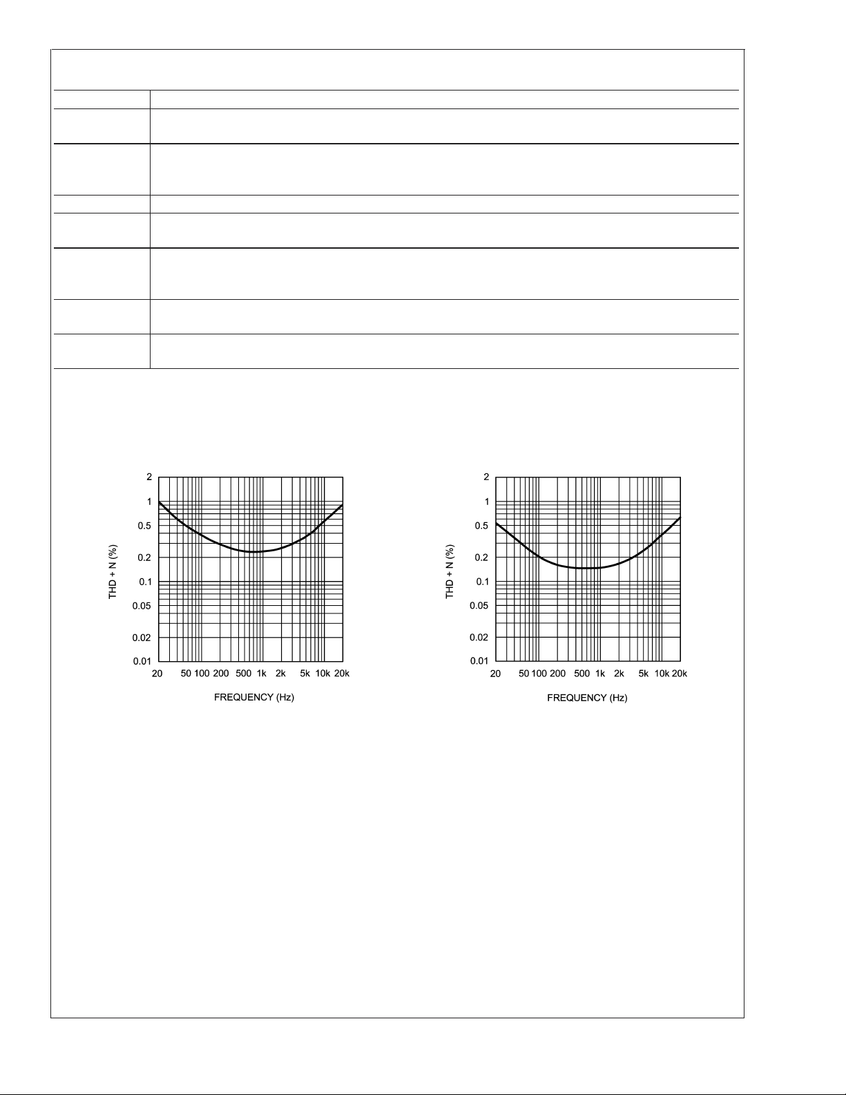
Typical Performance Characteristics
LM4908
.
i
THD+N vs Frequency
= 2.6V, PWR = 15mW, RL=8Ω
V
DD
20075267
THD+N vs Frequency
VDD= 2.6V, PWR = 15mW, RL=16Ω
20075268
www.national.com5
Page 6
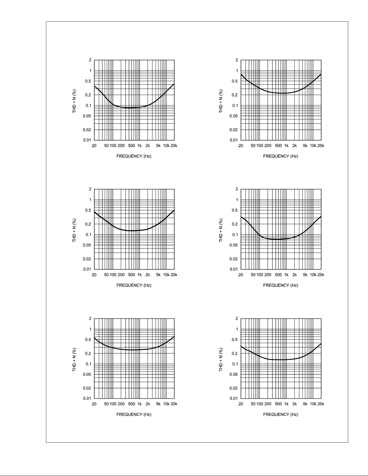
Typical Performance Characteristics (Continued)
LM4908
THD+N vs Frequency
V
= 2.6V, PWR = 15mW, RL=32Ω
DD
THD+N vs Frequency
= 3.3V, PWR = 25mW, RL=16Ω
V
DD
THD+N vs Frequency
VDD= 3.3V, PWR = 25mW, RL=8Ω
20075269 20075270
THD+N vs Frequency
VDD= 3.3V, PWR = 25mW, RL=32Ω
20075271 20075272
THD+N vs Frequency
= 5V, PWR = 50mW, RL=8Ω
V
DD
20075273 20075274
www.national.com 6
THD+N vs Frequency
VDD= 5V, PWR = 50mW, RL=16Ω
Page 7
Typical Performance Characteristics (Continued)
LM4908
THD+N vs Frequency
V
= 5V, PWR = 50mW, RL=32Ω
DD
THD+N vs Output Power
= 2.6V, RL=8Ω, f = 1kHz
V
DD
THD+N vs Frequency
VDD= 5V, V
20075275 20075276
= 3.5Vpp,RL=5kΩ
OUT
THD+N vs Output Power
VDD= 2.6V, RL=16Ω, f = 1kHz
THD+N vs Output Power
= 2.6V, RL=32Ω, f = 1kHz
V
DD
20075277 20075278
THD+N vs Output Power
VDD= 3.3V, RL=8Ω, f = 1kHz
20075279 20075280
www.national.com7
Page 8

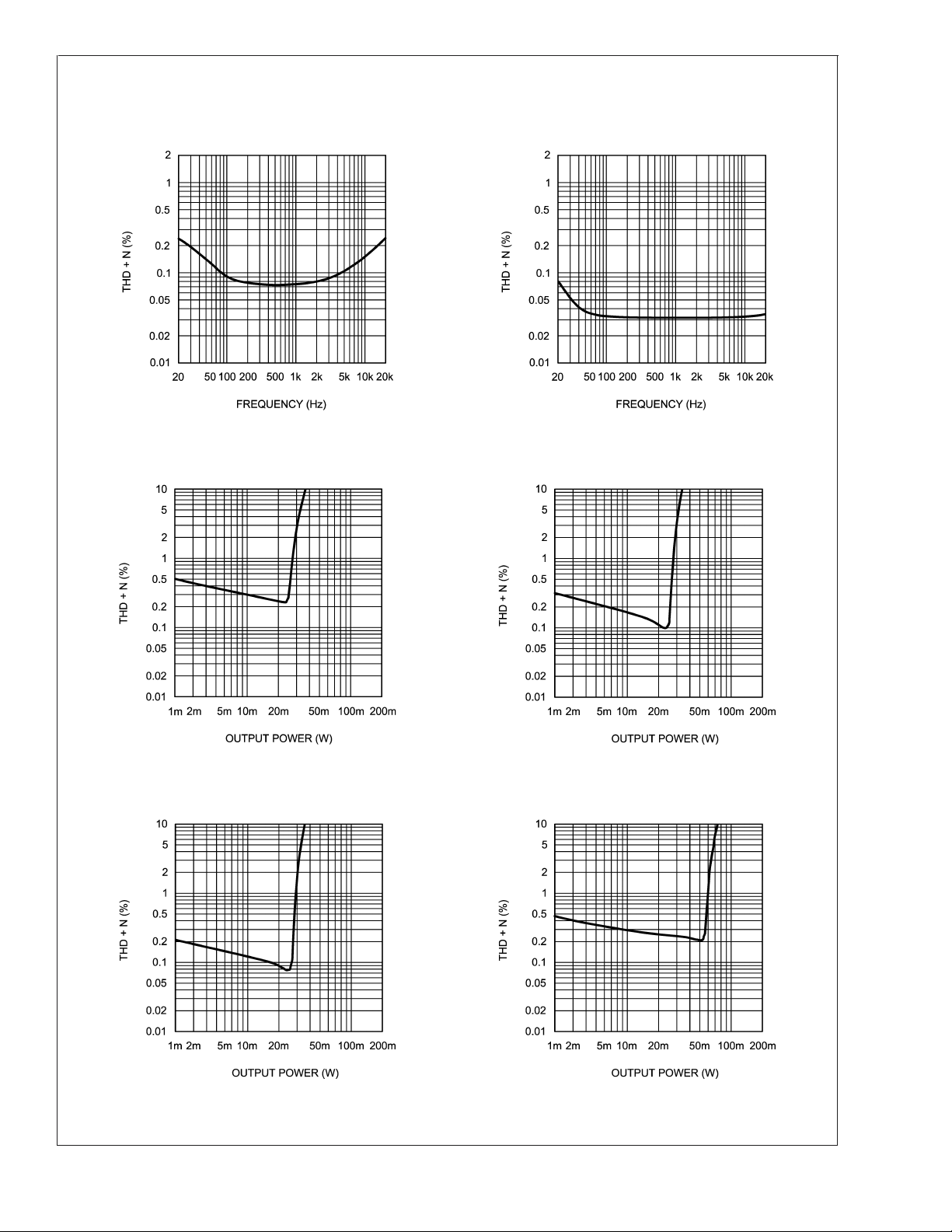
Typical Performance Characteristics (Continued)
LM4908
THD+N vs Output Power
V
= 3.3V, RL=16Ω, f = 1kHz
DD
THD+N vs Output Power
= 5V, RL=8Ω, f = 1kHz
V
DD
THD+N vs Output Power
VDD= 3.3V, RL=32Ω, f = 1kHz
20075281 20075282
THD+N vs Output Power
VDD= 5V, RL=16Ω, f = 1kHz
20075283 20075284
THD+N vs Output Power
= 5V, RL=32Ω, f = 1kHz
V
DD
20075285
www.national.com 8
Output Power vs Load Resistance
VDD= 2.6V, f = 1kHz
20075286
Page 9

Typical Performance Characteristics (Continued)
LM4908
Output Power vs Load Resistance
V
= 3.3V, f = 1kHz
DD
Output Power vs Supply Voltage
=8Ω, f = 1kHz
R
L
Output Power vs Load Resistance
VDD= 5V, f = 1kHz
20075287 20075288
Output Power vs Supply Voltage
RL=16Ω, f = 1kHz
Output Power vs Supply Voltage
=32Ω, f = 1kHz
R
L
20075289 20075290
Clipping Voltage vs
Supply Voltage
20075291
20075292
www.national.com9
Page 10

Typical Performance Characteristics (Continued)
LM4908
Power Dissipation vs
Output Power
Power Dissipation vs
Output Power
20075229
Power Dissipation vs
Output Power
Crosstalk vs Frequency
= 5V, RL=8Ω
V
DD
20075230
Crosstalk vs Frequency
= 5V, RL=32Ω
V
DD
20075231
20075294
20075293
Output Noise vs Frequency
VDD= 5V, RL=32Ω
20075295
www.national.com 10
Page 11

Typical Performance Characteristics (Continued)
LM4908
PSRR vs Frequency
V
= 5V, RL=32Ω,V
DD
RIPPLE
= 100mV
pp
Pins 3 and 5 directly driven, Inputs Floating
20075296
Open Loop Frequency Response
= 5V, RL=8Ω
V
DD
PSRR vs Frequency
V
= 5V, RL=32Ω,V
DD
RIPPLE
Inputs Terminated
Open Loop Frequency Response
VDD= 5V, RL=32Ω
= 100mV
20075297
pp
Open Loop Frequency Response
= 5V, RL=5kΩ
V
DD
20075298
200752A0
20075299
Supply Current vs
Supply Voltage (no Load)
200752A1
www.national.com11
Page 12

Typical Performance Characteristics (Continued)
LM4908
Frequency Response vs
Output Capacitor Size
Frequency Response vs
Output Capacitor Size
Frequency Response vs
Output Capacitor Size
20075245 20075246
Typical Application
Frequency Response
20075247 20075248
Typical Application
Frequency Response
20075249
www.national.com 12
Page 13

Application Information
EXPOSED-DAP PACKAGE PCB MOUNTING CONSIDERATION
The LM4908’s exposed-dap (die attach paddle) package
(LQ) provides a low thermal resistance between the die and
the PCB to which the part is mounted and soldered. This
allows rapid heat transfer from the die to the surrounding
PCB copper traces, ground plane, and surrounding air.
The LQ package should have its DAP soldered to a copper
pad on the PCB. The DAP’s PCB copper pad may be connected to a large plane of continuous unbroken copper. This
plane forms a thermal mass, heat sink, and radiation area.
However, since the LM4908 is designed for headphone applications, connecting a copper plane to the DAP’s PCB
copper pad is not required. The LM4908’s Power Dissipation
vs Output Power Curve in the Typical Performance Char-
acteristics shows that the maximum power dissipated is just
45mW per amplifier with a 5V power supply and a 32Ω load.
Further detailed and specific information concerning PCB
layout, fabrication, and mounting an LQ (LLP) package is
available from National Semiconductor’s Package Engineering Group under application note AN1187.
POWER DISSIPATION
Power dissipation is a major concern when using any power
amplifier and must be thoroughly understood to ensure a
successful design. Equation 1 states the maximum power
dissipation point for a single-ended amplifier operating at a
given supply voltage and driving a specified output load.
=(VDD)2/(2π2RL) (1)
P
DMAX
Since the LM4908 has two operational amplifiers in one
package, the maximum internal power dissipation point is
twice that of the number which results from Equation 1. Even
with the large internal power dissipation, the LM4908 does
not require heat sinking over a large range of ambient temperature. From Equation 1, assuming a 5V power supply and
a32Ω load, the maximum power dissipation point is 40mW
per amplifier. Thus the maximum package dissipation point
is 80mW. The maximum power dissipation point obtained
must not be greater than the power dissipation that results
from Equation 2:
=(T
P
DMAX
JMAX−TA
For package MUA08A, θJA= 210˚C/W. T
the LM4908. Depending on the ambient temperature, T
the system surroundings, Equation 2 can be used to find the
maximum internal power dissipation supported by the IC
packaging. If the result of Equation 1 is greater than that of
Equation 2, then either the supply voltage must be decreased, the load impedance increased or T
the typical application of a 5V power supply, with a 32Ω load,
the maximum ambient temperature possible without violating
the maximum junction temperature is approximately 133.2˚C
provided that device operation is around the maximum
power dissipation point. Power dissipation is a function of
output power and thus, if typical operation is not around the
maximum power dissipation point, the ambient temperature
may be increased accordingly. Refer to the Typical Perfor-
mance Characteristics curves for power dissipation information for lower output powers.
)/θ
JA
JMAX
= 150˚C for
reduced. For
A
A
(2)
,of
POWER SUPPLY BYPASSING
As with any power amplifier, proper supply bypassing is
critical for low noise performance and high power supply
rejection. Applications that employ a 5V regulator typically
use a 10µF in parallel with a 0.1µF filter capacitors to stabilize the regulator’s output, reduce noise on the supply line,
and improve the supply’s transient response. However, their
presence does not eliminate the need for a local 0.1µF
supply bypass capacitor, C
, connected between the
S
LM4908’s supply pins and ground. Keep the length of leads
and traces that connect capacitors between the LM4908’s
power supply pin and ground as short as possible. Connecting a 1.0µF capacitor, C
, between the IN A(+) / IN B(+) node
B
and ground improves the internal bias voltage’s stability and
improves the amplifier’s PSRR. The PSRR improvements
increase as the bypass pin capacitor value increases. Too
large, however, increases the amplifier’s turn-on time. The
selection of bypass capacitor values, especially C
, depends
B
on desired PSRR requirements, click and pop performance
(as explained in the section, Selecting Proper External
Components), system cost, and size constraints.
SELECTING PROPER EXTERNAL COMPONENTS
Optimizing the LM4908’s performance requires properly selecting external components. Though the LM4908 operates
well when using external components with wide tolerances,
best performance is achieved by optimizing component values.
The LM4908 is unity-gain stable, giving a designer maximum
design flexibility. The gain should be set to no more than a
given application requires. This allows the amplifier to
achieve minimum THD+N and maximum signal-to-noise ratio. These parameters are compromised as the closed-loop
gain increases. However, low gain demands input signals
with greater voltage swings to achieve maximum output
power. Fortunately, many signal sources such as audio
CODECs have outputs of 1V
RMS
(2.83V
). Please refer to
P-P
the Audio Power Amplifier Design section for more information on selecting the proper gain.
Input and Output Capacitor Value Selection
Amplifying the lowest audio frequencies requires high value
input and output coupling capacitors (C
and COin Figure 1).
I
A high value capacitor can be expensive and may compromise space efficiency in portable designs. In many cases,
however, the speakers used in portable systems, whether
internal or external, have little ability to reproduce signals
below 150Hz. Applications using speakers with this limited
frequency response reap little improvement by using high
value input and output capacitors.
Besides affecting system cost and size, C
has an effect on
i
the LM4908’s click and pop performance. The magnitude of
the pop is directly proportional to the input capacitor’s size.
Thus, pops can be minimized by selecting an input capacitor
value that is no higher than necessary to meet the desired
−3dB frequency.
As shown in Figure 1, the input resistor, R
capacitor, C
, produce a −3dB high pass filter cutoff fre-
I
and the input
I
quency that is found using Equation (3). In addition, the
output load R
, and the output capacitor CO, produce a -3db
L
high pass filter cutoff frequency defined by Equation (4).
f
f
O-3db
I-3db
=1/2πRIC
=1/2πRLC
I
O
(3)
(4)
LM4908
www.national.com13
Page 14

Application Information (Continued)
LM4908
Also, careful consideration must be taken in selecting a
certain type of capacitor to be used in the system. Different
types of capacitors (tantalum, electrolytic, ceramic) have
unique performance characteristics and may affect overall
system performance.
Bypass Capacitor Value
Besides minimizing the input capacitor size, careful consideration should be paid to the value of the bypass capacitor,
. Since CBdetermines how fast the LM4908 settles to
C
B
quiescent operation, its value is critical when minimizing
turn-on pops. The slower the LM4908’s outputs ramp to their
quiescent DC voltage (nominally 1/2 V
turn-on pop. Choosing C
equal to 1.0µF or larger, will
B
minimize turn-on pops. As discussed above, choosing C
larger than necessary for the desired bandwith helps minimize clicks and pops.
AUDIO POWER AMPLIFIER DESIGN
Design a Dual 70mW/32Ω Audio Amplifier
Given:
Power Output 70mW
Load Impedance 32Ω
Input Level 1Vrms (max)
Input Impedance 20kΩ
Bandwidth 100Hz–20kHz
The design begins by specifying the minimum supply voltage
necessary to obtain the specified output power. One way to
find the minimum supply voltage is to use the Output Power
vs Supply Voltage curve in the Typical Performance Char-
acteristics section. Another way, using Equation (5), is to
calculate the peak output voltage necessary to achieve the
desired output power for a given load impedance. To account for the amplifier’s dropout voltage, two additional voltages, based on the Dropout Voltage vs Supply Voltage in the
Typical Performance Characteristics curves, must be
added to the result obtained by Equation (5). For a singleended application, the result is Equation (6).
), the smaller the
DD
±
0.50dB
package. Once the power dissipation equations have been
addressed, the required gain can be determined from Equation (7).
(7)
Thus, a minimum gain of 1.497 allows the LM4908 to reach
full output swing and maintain low noise and THD+N perfromance. For this example, let A
The amplifiers overall gain is set using the input (R
feedback (R
) resistors. With the desired input impedance
f
V
= 1.5.
) and
i
set at 20kΩ, the feedback resistor is found using Equation
(8).
no
i
The value of R
is 30kΩ.
f
A
V=Rf/Ri
(8)
The last step in this design is setting the amplifier’s −3db
±
frequency bandwidth. To achieve the desired
0.25dB pass
band magnitude variation limit, the low frequency response
must extend to at lease one−fifth the lower bandwidth limit
and the high frequency response must extend to at least five
times the upper bandwidth limit. The gain variation for both
±
response limits is 0.17dB, well within the
0.25dB desired
limit. The results are an
= 100Hz/5 = 20Hz (9)
f
L
and a
= 20kHz*5 = 100kHz (10)
f
H
As stated in the External Components section, both R
conjunction with C
, and Cowith RL, create first order high-
i
in
i
pass filters. Thus to obtain the desired low frequency re-
±
sponse of 100Hz within
0.5dB, both poles must be taken
into consideration. The combination of two single order filters
at the same frequency forms a second order response. This
results in a signal which is down 0.34dB at five times away
from the single order filter −3dB point. Thus, a frequency of
(5)
20Hz is used in the following equations to ensure that the
response is better than 0.5dB down at 100Hz.
≥ (2V
V
DD
OPEAK
+(V
OD
TOP
+V
OD
BOT
)) (6)
The Output Power vs Supply Voltage graph for a 32Ω load
indicates a minimum supply voltage of 4.8V. This is easily
met by the commonly used 5V supply voltage. The additional
voltage creates the benefit of headroom, allowing the
LM4908 to produce peak output power in excess of 70mW
without clipping or other audible distortion. The choice of
supply voltage must also not create a situation that violates
maximum power dissipation as explained above in the
Power Dissipation section. Remember that the maximum
power dissipation point from Equation (1) must be multiplied
by two since there are two independent amplifiers inside the
www.national.com 14
≥ 1/(2π *20kΩ * 20 Hz) = 0.397µF; use 0.39µF.
C
i
Co≥ 1/(2π *32Ω * 20 Hz) = 249µF; use 330µF.
The high frequency pole is determined by the product of the
desired high frequency pole, f
. With a closed-loop gain of 1.5 and fH= 100kHz, the
A
V
, and the closed-loop gain,
H
resulting GBWP = 150kHz which is much smaller than the
LM4908’s GBWP of 3MHz. This figure displays that if a
designer has a need to design an amplifier with a higher
gain, the LM4908 can still be used without running into
bandwidth limitations.
Page 15

Demonstration Board Layout
LM4908
Recommended MSOP Board Layout:
Top Overlay
Recommended MSOP Board Layout:
Top Layer
20075264
20075265
Recommended MSOP Board Layout:
Bottom Layer
20075266
www.national.com15
Page 16

Demonstration Board Layout (Continued)
LM4908
Recommended LQ Board Layout:
Top Overlay
Recommended LQ Board Layout:
Top Layer
200752B1
200752B0
Recommended LQ Board Layout:
Bottom Layer
www.national.com 16
200752A9
Page 17

Demonstration Board Layout (Continued)
LM4908
Recommended MA Board Layout:
Top Overlay
Recommended MA Board Layout:
Top Layer
200752B4
200752B3
Recommended MA Board Layout:
Bottom Layer
200752B2
www.national.com17
Page 18

LM4908 MDC MWC Dual 120MW Headphone Amplifier
LM4908
Die Layout (A - Step)
DIE/WAFER CHARACTERISTICS
Fabrication Attributes General Die Information
Physical Die Identification LM4908A Bond Pad Opening Size (min) 70µm x 70µm
Die Step A Bond Pad Metalization ALUMINUM
Physical Attributes Passivation NITRIDE
Wafer Diameter 150mm Back Side Metal BARE BACK
Dise Size (Drawn) 889µm x 622µm
35.0mils x 24.5mils
Thickness 216µm Nominal
Min Pitch 216µm Nominal
Special Assembly Requirements:
Note: Actual die size is rounded to the nearest micron.
Die Bond Pad Coordinate Locations (A - Step)
(Referenced to die center, coordinates in µm) NC = No Connection, N.U. = Not Used
SIGNAL NAME PAD# NUMBER
INPUT B+ 1 -367 232 70 x 70
INPUT B- 2 -367 15 70 x 70
OUTPUT B 3 -367 -232 70 x 70
VDD 4 35 -232 155 x 70
OUTPUT A 5 367 -232 70 x 70
INPUT A- 6 367 15 70 x 70
INPUT A+ 7 367 232 70 x 70
GND 8 68 232 155 x 70
X/Y COORDINATES PAD SIZE
XYX Y
20075263
Back Side Connection Floating
www.national.com 18
Page 19

LM4908 MDC MWC
Dual 120MW Headphone Amplifier
IN U.S.A
Tel #: 1 877 Dial Die 1 877 342 5343
Fax: 1 207 541 6140
IN EUROPE
Tel: 49 (0) 8141 351492 / 1495
Fax: 49 (0) 8141 351470
IN ASIA PACIFIC
Tel: (852) 27371701
IN JAPAN
Tel: 81 043 299 2308
LM4908
(Continued)
www.national.com19
Page 20

Physical Dimensions inches (millimeters)
unless otherwise noted
LM4908
Order Number LM4908LQ
NS Package Number LQB08A
Order Number LM4908MA
NS Package Number M08A
www.national.com 20
Page 21

Physical Dimensions inches (millimeters) unless otherwise noted (Continued)
10kV ESD Rated, Dual 120 mW Headphone Amplifier
Order Number LM4908MM
NS Package Number MUA08A
LIFE SUPPORT POLICY
NATIONAL’S PRODUCTS ARE NOT AUTHORIZED FOR USE AS CRITICAL COMPONENTS IN LIFE SUPPORT
DEVICES OR SYSTEMS WITHOUT THE EXPRESS WRITTEN APPROVAL OF THE PRESIDENT AND GENERAL
COUNSEL OF NATIONAL SEMICONDUCTOR CORPORATION. As used herein:
1. Life support devices or systems are devices or
systems which, (a) are intended for surgical implant
into the body, or (b) support or sustain life, and
whose failure to perform when properly used in
accordance with instructions for use provided in the
2. A critical component is any component of a life
support device or system whose failure to perform
can be reasonably expected to cause the failure of
the life support device or system, or to affect its
safety or effectiveness.
labeling, can be reasonably expected to result in a
significant injury to the user.
BANNED SUBSTANCE COMPLIANCE
National Semiconductor certifies that the products and packing materials meet the provisions of the Customer Products
Stewardship Specification (CSP-9-111C2) and the Banned Substances and Materials of Interest Specification
(CSP-9-111S2) and contain no ‘‘Banned Substances’’ as defined in CSP-9-111S2.
National Semiconductor
Americas Customer
Support Center
Email: new.feedback@nsc.com
Tel: 1-800-272-9959
www.national.com
National does not assume any responsibility for use of any circuitry described, no circuit patent licenses are implied and National reserves the right at any time without notice to change said circuitry and specifications.
National Semiconductor
Europe Customer Support Center
Fax: +49 (0) 180-530 85 86
Email: europe.support@nsc.com
Deutsch Tel: +49 (0) 69 9508 6208
English Tel: +44 (0) 870 24 0 2171
Français Tel: +33 (0) 1 41 91 8790
National Semiconductor
Asia Pacific Customer
Support Center
Email: ap.support@nsc.com
National Semiconductor
Japan Customer Support Center
Fax: 81-3-5639-7507
Email: jpn.feedback@nsc.com
Tel: 81-3-5639-7560
 Loading...