

February 14, 2008
LM48860
Ground-Referenced, Ultra Low Noise, Fixed Gain Stereo
Headphone Amplifier
LM48860 Ground-Referenced, Ultra Low Noise, Fixed Gain Stereo Headphone Amplifier
General Description
The LM48860 is a ground referenced, fixed-gain audio power
amplifier capable of delivering 40mW per channel of continuous average power into a 16Ω single-ended load with less
than 1% THD+N from a 3V power supply.
The LM48860 features a new circuit technology that utilizes
a charge pump to generate a negative reference voltage. This
allows the outputs to be biased about ground, thereby eliminating output-coupling capacitors typically used with normal
single-ended loads.
Boomer audio power amplifiers were designed specifically to
provide high quality output power with a minimal amount of
external components. The LM48860 does not require output
coupling capacitors or bootstrap capacitors, and therefore is
ideally suited for mobile phone and other low voltage applications where minimal power consumption is a primary requirement.
The LM48860 features a low-power consumption shutdown
mode selectable for either channel separately. This is accomplished by driving either the SD_RC
nel) or SD_LC (Shutdown Left Channel) (or both) pins with
logic low, depending on which channel is desired shutdown.
Additionally, the LM48860 features an internal thermal shutdown protection mechanism.
The LM48860 contains advanced pop & click circuitry that
eliminates noises which would otherwise occur during turn-on
and turn-off transitions.
The LM48860 has an internal fixed gain of 1.5V/V.
(Shutdown Right Chan-
Key Specifications
■ PSRR at 217Hz (V
■ Stereo Power Output at V
RL = 16Ω, THD+N = 1%
■ Shutdown Current
■ Internal Fixed Gain
■ Operating Voltage
DD
= 3.0V)
DD
= 3V,
40mW (typ)
0.1μA (typ)
1.5V/V (typ)
2.0V to 5.5V
Features
Fixed logic levels with supply voltage
■
Ground referenced outputs
■
High PSRR
■
Available in space-saving micro SMD package
■
Ultra low current shutdown mode
■
Improved pop & click circuitry eliminates noises during
■
turn-on and turn-off transitions
No output coupling capacitors, snubber networks,
■
bootstrap capacitors, or gain-setting resistors required
Shutdown either channel independently
■
Applications
Mobile Phones
■
MP3 Players
■
PDAs
■
Portable electronic devices
■
Notebook PCs
■
80dB (typ)
Boomer® is a registered trademark of National Semiconductor Corporation.
© 2008 National Semiconductor Corporation 300068 www.national.com
Typical Application
LM48860
FIGURE 1. Typical Audio Amplifier Application Circuit
30006889
www.national.com 2
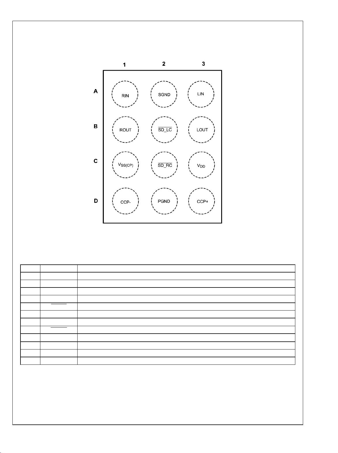
Connection Diagram
LM48860
LM48860TL Pinout
(BUMP DOWN VIEW )
Order Number LM48860TL
See NS Package Number TLA12XXX
Top View
Pin Descriptions
Pin Name Function
A1 RIN Right Channel Input
A2 SGND Signal Ground
A3 LIN Left Channel Input
B1 ROUT Right Channel Output
B2 SD_LC Active Low Shutdown, Left Channel
B3 LOUT Left Channel Output
C1 V
C2 SD_RC Active-Low Shutdown, Right Channel
C3 V
D1 CCP- Negative Terminal - Charge Pump Flying Capacitor
D2 PGND Power Ground
D3 CCP+ Positive Terminal - Charge Pump Flying Capacitor
SS(CP)
DD
Charge Pump Voltage Output
Supply Voltage
30006813
3 www.national.com
Absolute Maximum Ratings (Notes 2, 2)
If Military/Aerospace specified devices are required,
LM48860
please contact the National Semiconductor Sales Office/
Junction Temperature 150°C
Thermal Resistance
θJA (typ) TLA12XXX (Note 11)
Distributors for availability and specifications.
Supply Voltage 6.0V
Storage Temperature −65°C to +150°C
Input Voltage
-0.3V to V
DD
Power Dissipation (Note 3) Internally Limited
Operating Ratings
Temperature Range
T
≤ TA ≤ T
MIN
Supply Voltage (VDD) 2.0V ≤ VDD ≤ 5.5V
MAX
ESD Rating(Note 4) 2000V
ESD Rating (Note 5) 200V
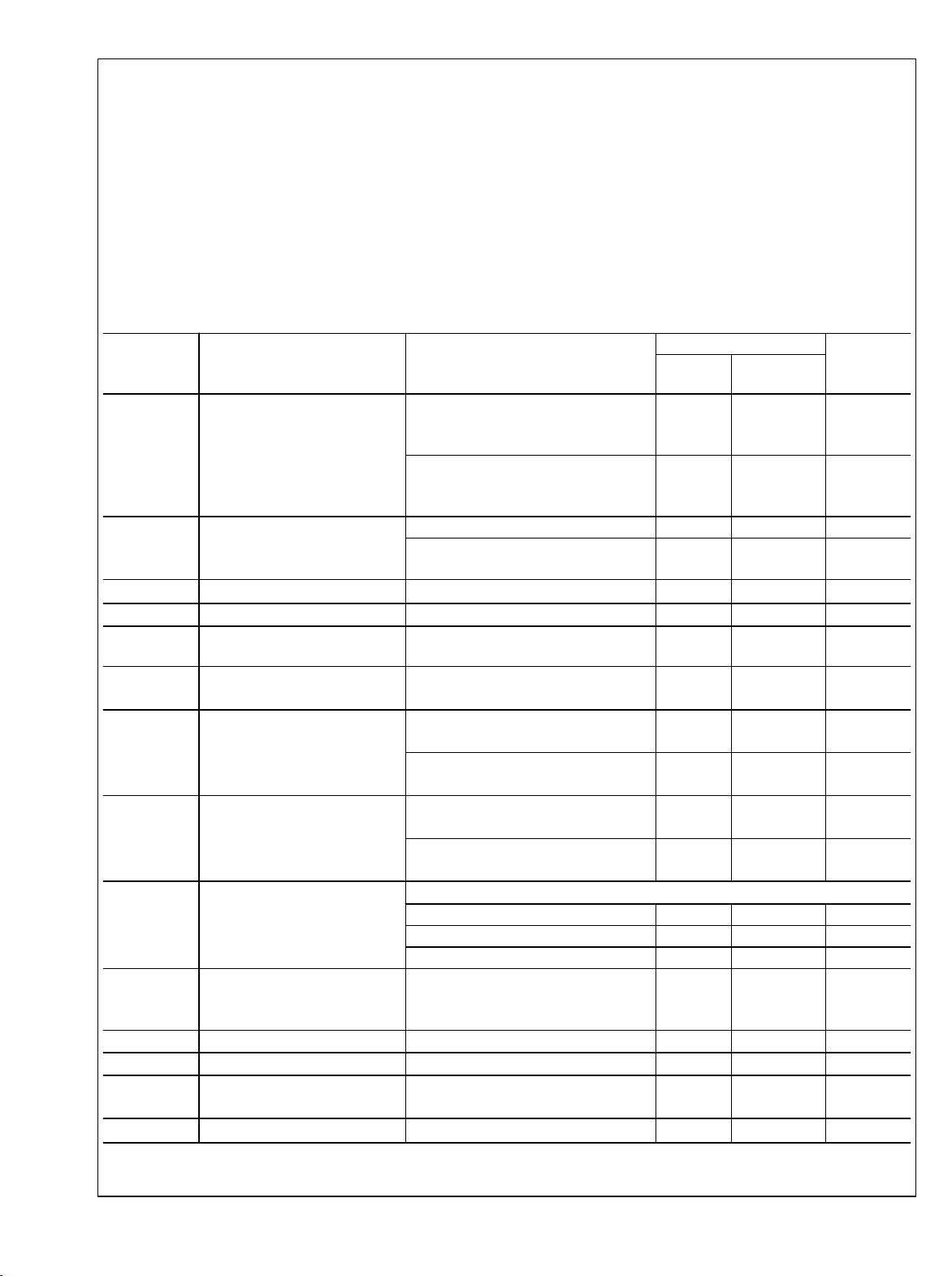
Electrical Characteristics VDD = 3V (Notes 1, 2)
The following specifications apply for VDD = 3V and 16Ω load unless otherwise specified. Limits apply to TA = 25°C.
LM48860
Symbol Parameter Conditions
VDD = 3.0V,
VIN = 0V, inputs terminated
I
DD
Quiescent Power Supply Current
Full Power Mode
both channels enabled
VDD = 5.0V,
VIN = 0V, inputs terminated
both channels enabled
SD_LC = SD_RC= GND 0.1 1 µA (max)
I
SD
Shutdown Current
SD_LC = SD_RC= GND,
VDD = 5.0V
V
A
ΔA
OS
V
V
Output Offset Voltage
Voltage Gain
Channel-to-channel Gain
RL = 32Ω, VIN = 0V
1 %
Matching
R
IN
Input Resistance
THD+N = 1% (max); f = 1kHz,
P
O
Output Power
RL = 16Ω, (two channels in phase)
THD+N = 1% (max); f = 1kHz,
RL = 32Ω, (two channels in phase)
PO = 20mW, f = 1kHz, RL = 16Ω
THD+N
Total Harmonic Distortion +
Noise
(two channels in phase)
PO = 25mW, f = 1kHz, RL = 32Ω
(two channels in phase)
V
= 200mVPP, Input Referred
RIPPLE
PSRR
Power Supply Rejection Ratio
Full Power Mode
f = 217Hz 80 73 dB (min)
f = 1kHz 75 dB
f = 20kHz 60 dB
SNR Signal-to-Noise Ratio
RL = 32Ω, P
f = 1kHz, BW = 20Hz to 22kHz,
= 50mW,
OUT
A-weighted
V
V
X
∈
IH
IL
TALK
OS
Shutdown Input Voltage High
Shutdown Input Voltage Low
Crosstalk
Output Noise
VDD = 2.0V to 5.5V
VDD = 2.0V to 5.5V
RL = 16Ω, PO = 1.6mW,
f = 1kHz
A-weighted filter, VIN = 0V
Typical
(Note 6)
4 5.5 mA (max)
4.2 mA
0.1 1 µA (max)
0.7 5.5
–1.5
20
40 35 mW (min)
50 40 mW (min)
0.025
0.014
105 dB
75
8
59.3°C/W
−40°C ≤ TA ≤ 85°C
Limit
(Note 7)
Units
(Limits)
mV (max)
15
25
kΩ (min)
kΩ (max)
1.2 V (min)
0.45 V (max)
V/V
%
%
dB
μV
www.national.com 4
LM48860
Symbol Parameter Conditions
Typical
(Note 6)
LM48860
Limit
(Note 7)
Units
(Limits)
VSD = GND
Z
OUT
I
L
Note 1: “Absolute Maximum Ratings” indicate limits beyond which damage to the device may occur, including inoperability and degradation of device reliability
and/or performance. Functional operation of the device and/or non-degradation at the Absolute Maximum Ratings or other conditions beyond those indicated in
the Recommended Operating Conditions is not implied. The Recommended Operating Conditions indicate conditions at which the device is functional and the
device should not be operated beyond such conditions. All voltages are measured with respect to the ground pin, unless otherwise specified
Note 2: The Electrical Characteristics tables list guaranteed specifications under the listed Recommended Operating Conditions except as otherwise modified
or specified by the Electrical Characteristics Conditions and/or Notes. Typical specifications are estimations only and are not guaranteed.
Note 3: The maximum power dissipation must be derated at elevated temperatures and is dictated by T
allowable power dissipation is P
derating curves for additional information.
Note 4: Human body model, applicable std. JESD22-A114C.
Note 5: Machine model, applicable std. JESD22-A115-A.
Note 6: Typical values represent most likely parametric norms at TA = +25ºC, and at the Recommended Operation Conditions at the time of product
characterization and are not guaranteed.
Note 7: Datasheet min/max specification limits are guaranteed by test or statistical analysis.
Note 8: θJA value is measured with the device mounted on a PCB with a 1.5” x 1.375”, 1oz copper heatsink.
Output Impedance
Input Leakage ±0.1 nA
= (T
DMAX
- TA) / θJA or the number given in Absolute Maximum Ratings, whichever is lower. For the LM48860, see power
JMAX
Input Terminated
Input not terminated
SD_LC = SD_RC = GND
30
30
, θJA, and the ambient temperature, TA. The maximum
JMAX
20
kΩ (min)
External Components Description
(Figure 1)
Components Functional Description
Input coupling capacitor which blocks the DC voltage at the amplifier’s input terminals. Also creates a high passpass filter with Ri at fC = 1/(2RiC1). Refer to the section Proper Selection of External Components, for an
1.
2.
3.
4.
5.
6.
C
1
explanation of how to determine the value of C1.
Input coupling capacitor which blocks the DC voltage at the amplifier’s input terminals. Also creates a high passpass filter with Ri at fC = 1/(2RiC2). Refer to the Power Supply Bypassing section for an explanation of how to
C
2
determine the value of C2.
C
Output capacitor. Low ESR ceramic capacitor (≤100mΩ)
3
C
Flying capacitor. Low ESR ceramic capacitor (≤100mΩ)
4
Tantalum capacitor. Supply bypass capacitor which provides power supply filtering. Refer to the Power Supply
C
5
Bypassing section for information concerning proper placement and selection of the supply bypass capacitor.
Ceramic capacitor. Supply bypass capacitor which provides power supply filtering. Refer to the Power Supply
C
6
Bypassing section for information concerning proper placement and selection of the supply bypass capacitor.
kΩ
5 www.national.com

Typical Performance Characteristics
LM48860
THD+N vs Output Power
VDD = 3V, RL = 16Ω
f = 1kHz, 22kHz BW, one channel enabled
300068d2
THD+N vs Output Power
VDD = 3V, RL = 32Ω
f = 1kHz, 22kHz BW, one channel enabled
THD+N vs Output Power
VDD = 3V, RL = 16Ω, f = 1kHz
22kHz BW, two channels in phase
30006824
THD+N vs Output Power
VDD = 3V, RL = 32Ω, f = 1kHz
22kHz BW, two channels in phase
300068d3
THD+N vs Output Power
VDD = 3.6V, RL = 16Ω
f = 1kHz, 22kHz BW, one channel enabled
300068c8
www.national.com 6
30006825
THD+N vs Output Power
VDD = 3.6V, RL = 16Ω, f = 1kHz
22kHz BW, two channels in phase
300068c9

LM48860
THD+N vs Output Power
VDD = 3.6V, RL = 32Ω
f = 1kHz, 22kHz BW, one channel enabled
300068d0
THD+N vs Output Power
VDD = 4.2V, RL = 16Ω
f = 1kHz, 22kHz BW, one channel enabled
THD+N vs Output Power
VDD = 3.6V, RL = 32Ω, f = 1kHz
22kHz BW, two channels in phase
300068d1
THD+N vs Output Power
VDD = 4.2V, RL = 16Ω, f = 1kHz
22kHz BW, two channels in phase
300068d4
THD+N vs Output Power
VDD = 4.2V, RL = 32Ω
f = 1kHz, 22kHz BW, one channel enabled
300068d6
300068d5
THD+N vs Output Power
VDD = 4.2V, RL = 32Ω, f = 1kHz
22kHz BW, two channels in phase
300068d7
7 www.national.com
LM48860
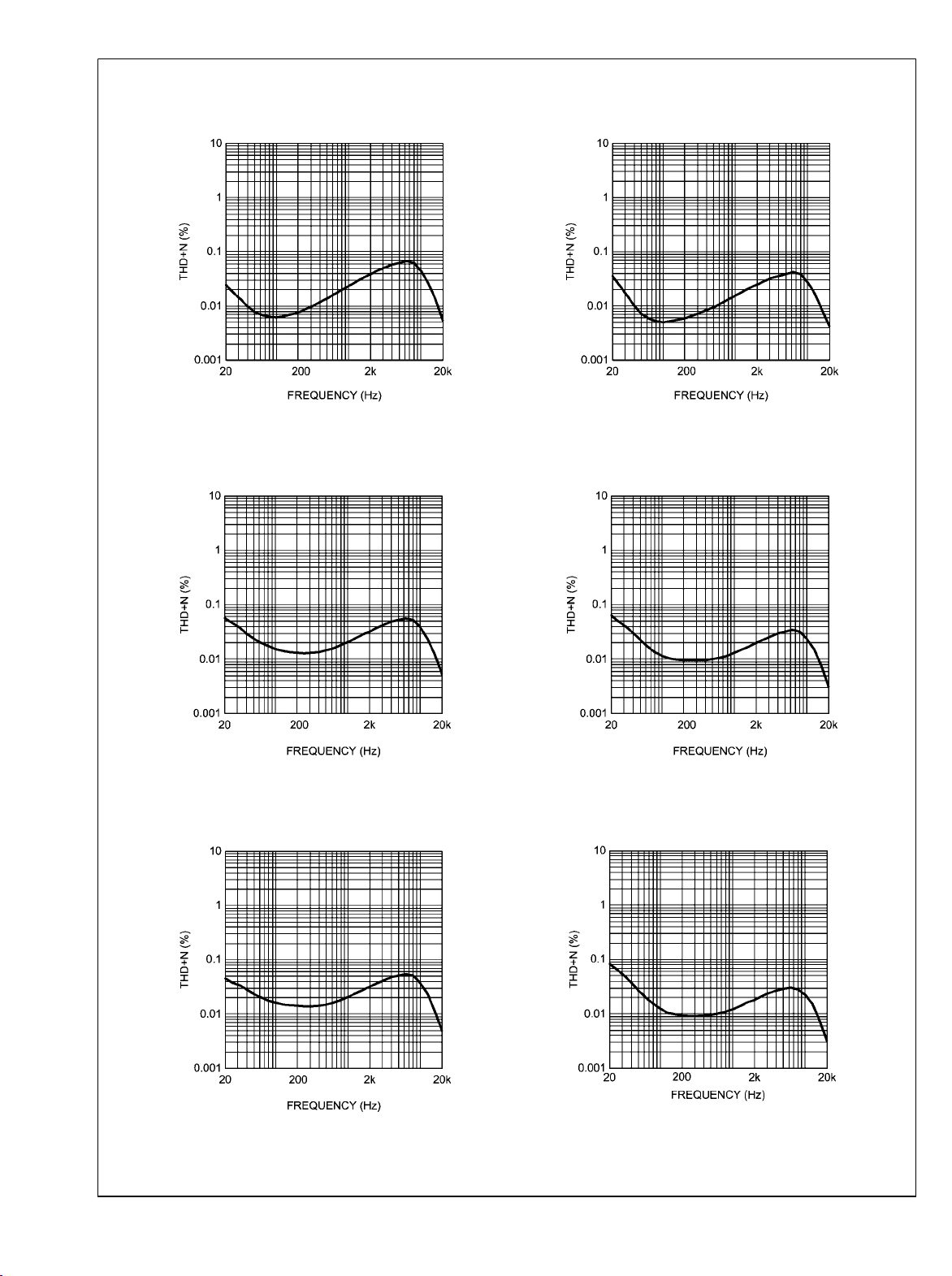
THD+N vs Frequency
VDD = 3V, RL = 16Ω
PO = 20mW, 22kHz BW
THD+N vs Frequency
VDD = 3V, RL = 32Ω
PO = 20mW, 22kHz BW
THD+N vs Frequency
VDD = 3.6V, RL = 16Ω
PO = 30mW, 22kHz BW
THD+N vs Frequency
VDD = 4.2V, RL = 16Ω
PO = 30mW, 22kHz BW
30006822
300068c4
30006823
THD+N vs Frequency
VDD = 3.6V, RL = 32Ω
PO = 30mW, 22kHz BW
300068c5
THD+N vs Frequency
VDD = 4.2V, RL = 32Ω
PO = 30mW, 22kHz BW
300068c6
www.national.com 8
300068c7
LM48860
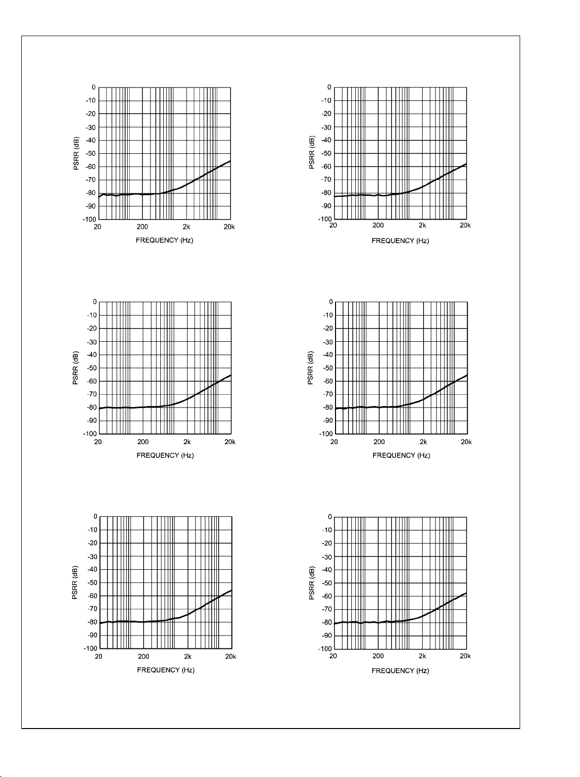
PSRR vs Frequency
VDD = 3V, RL = 16Ω
V
= 200mV
RIPPLE
PP
PSRR vs Frequency
VDD = 3.6V, RL = 16Ω
V
= 200mV
RIPPLE
PP
30006887
PSRR vs Frequency
VDD = 3V, RL = 32Ω
V
= 200mV
RIPPLE
PP
PSRR vs Frequency
VDD = 3.6V, RL = 32Ω
V
= 200mV
RIPPLE
PP
30006888
PSRR vs Frequency
VDD = 4.2V, RL = 16Ω
V
= 200mV
RIPPLE
PP
300068c0
300068c2
300068c1
PSRR vs Frequency
VDD = 4.2V, RL = 32Ω
V
= 200mV
RIPPLE
9 www.national.com
PP
300068c3
LM48860
Output Power vs Supply Voltage
RL = 16Ω, f = 1kHz, 22kHz BW
Output Power vs Supply Voltage
RL = 32Ω, f = 1kHz, 22kHz BW
30006885
Power Dissipation vs Output Power
VDD = 3V, RL = 16Ω, f = 1kHz
30006894
Power Dissipation vs Output Power
VDD = 5V, RL = 16Ω, f = 1kHz
30006886
Power Dissipation vs Output Power
VDD = 3V, RL = 32Ω, f = 1kHz
30006895
Power Dissipation vs Output Power
VDD = 5V, RL = 32Ω, f = 1kHz
30006896
www.national.com 10
30006897

LM48860
Supply Current vs Supply Voltage
VIN = GND, No Load
Power Derating Curve
VDD = 3V, RL = 32Ω
30006898
Power Derating Curve
VDD = 3V, RL = 16Ω
30006890
Power Derating Curve
VDD = 5V, RL = 16Ω
Power Derating Curve
VDD = 5V, RL = 32Ω
30006891
30006893
30006892
11 www.national.com
Application Information
SUPPLY VOLTAGE SEQUENCING
LM48860
It is a good general practice to first apply the supply voltage
to a CMOS device before any other signal or supply on other
pins. This is also true for the LM48860 audio amplifier which
is a CMOS device.
Before applying any signal to the inputs or shutdown pins of
the LM48860, it is important to apply a supply voltage to the
VDD pins. After the device has been powered, signals may be
applied to the shutdown pins (see MICRO POWER SHUTDOWN) and input pins.
ELIMINATING THE OUTPUT COUPLING CAPACITOR
The LM48860 features a low noise inverting charge pump that
generates an internal negative supply voltage. This allows the
outputs of the LM48860 to be biased about GND instead of a
nominal DC voltage, like traditional headphone amplifiers.
Because there is no DC component, the large DC blocking
capacitors (typically 220µF) are not necessary. The coupling
capacitors are replaced by two, small ceramic charge pump
capacitors, saving board space and cost.
Eliminating the output coupling capacitors also improves low
frequency response. In traditional headphone amplifiers, the
headphone impedance and the output capacitor form a high
pass filter that not only blocks the DC component of the output, but also attenuates low frequencies, impacting the bass
response. Because the LM48860 does not require the output
coupling capacitors, the low frequency response of the device
is not degraded by external components.
In addition to eliminating the output coupling capacitors, the
ground referenced output nearly doubles the available dynamic range of the LM48860 when compared to a traditional
headphone amplifier operating from the same supply voltage.
OUTPUT TRANSIENT ('CLICK AND POPS') ELIMINATED
The LM48860 contains advanced circuitry that virtually eliminates output transients ('clicks and pops'). This circuitry prevents all traces of transients when the supply voltage is first
applied or when the part resumes operation after coming out
of shutdown mode.
AMPLIFIER CONFIGURATION EXPLANATION
As shown in Figure 2, the LM48860 has two internal operational amplifiers. The two amplifiers have internally configured
gain.
Since this is an output ground-referenced amplifier, the
LM48860 does not require output coupling capacitors.
POWER DISSIPATION
From the graph (THD+N vs Output Power , VDD = 3V, RL =
16Ω, f = 1kHz, 22kH BW, two channels in phase, page 6)
assuming a 3V power supply and a 16Ω load, the maximum
power dissipation point and thus the maximum package dissipation point is 281mW. The maximum power dissipation
point obtained must not be greater than the power dissipation
that results from Equation 1.
P
= (T
DMAX
For the micro SMD package θ
for the LM48860. Depending on the ambient temperature,
TA, of the system surroundings, Equation 1 can be used to
find the maximum internal power dissipation supported by the
IC packaging. If the maximum power dissipation from the
- TA) / (θJA) (1)
JMAX
= 59.3°C/W. T
JA
JMAX
= 150°C
graph is greater than that of Equation 1, then either the supply
voltage must be decreased, the load impedance increased or
TA reduced (see power derating curves). For the application
of a 5V power supply, with a 16Ω load, the maximum ambient
temperature possible without violating the maximum junction
temperature is approximately 110°C provided that device operation is around the maximum power dissipation point. Power dissipation is a function of output power and thus, if typical
operation is not around the maximum power dissipation point,
the ambient temperature may be increased accordingly.
POWER SUPPLY BYPASSING
As with any power amplifier, proper supply bypassing is critical for low noise performance and high power supply rejection. Applications that employ a 3V power supply typically use
a 4.7µF capacitor in parallel with a 0.1µF ceramic filter capacitor to stabilize the power supply's output, reduce noise on
the supply line, and improve the supply's transient response.
Keep the length of leads and traces that connect capacitors
between the LM48860's power supply pin and ground as short
as possible.
MICRO POWER SHUTDOWN
The voltage applied to the SD_LC (shutdown left channel) pin
and the SD_RC (shutdown right channel) pin controls the
LM48860’s shutdown function. When active, the LM48860’s
micropower shutdown feature turns off the amplifiers’ bias
circuitry, reducing the supply current. The trigger point is
0.45V for a logic-low level, and 1.2V for logic-high level. The
low 0.01µA (typ) shutdown current is achieved by applying a
voltage that is as near as ground a possible to the SD_LC/
SD_RC pins. A voltage that is higher than ground may increase the shutdown current. Do not let SD_LC/SD_RC float,
connect either to high or low.
SELECTING PROPER EXTERNAL COMPONENTS
Optimizing the LM48860's performance requires properly selecting external components. Though the LM48860 operates
well when using external components with wide tolerances,
best performance is achieved by optimizing component values.
Charge Pump Capacitor Selection
Use low ESR (equivalent series resistance) (<100mΩ) ceramic capacitors with an X7R dielectric for best performance.
Low ESR capacitors keep the charge pump output
impedance to a minimum, extending the headroom on the
negative supply. Higher ESR capacitors result in reduced
output power from the audio amplifiers.
Charge pump load regulation and output impedance are affected by the value of the flying capacitor (C4). A larger valued
C4 (up to 3.3uF) improves load regulation and minimizes
charge pump output resistance. Beyond 3.3uF, the switch-on
resistance dominates the output impedance.
The output ripple is affected by the value and ESR of the output capacitor (C3). Larger capacitors reduce output ripple on
the negative power supply. Lower ESR capacitors minimize
the output ripple and reduce the output impedance of the
charge pump.
The LM48860 charge pump design is optimized for 2.2uF, low
ESR, ceramic, flying and output capacitors.
Input Capacitor Value Selection
Amplifying the lowest audio frequencies requires high value
input coupling capacitors (C1 and C2 in Figure 1). A high value capacitor can be expensive and may compromise space
efficiency in portable designs. In many cases, however, the
www.national.com 12

LM48860
speakers used in portable systems, whether internal or external, have little ability to reproduce signals below 150Hz.
Applications using speakers with this limited frequency response reap little improvement by using high value input and
output capacitors.
As shown in Figure 1, the internal input resistor, Ri and the
input capacitors, C1 and C2, produce a -3dB high-pass filter
cutoff frequency that is found using Equation (2).
The value of R
tics tables.
f
= 1 / 2πRINC (Hz) (2)
i-3dB
can be found in the Electrical Characteris-
IN
13 www.national.com

Demonstration Board PCB Layout
LM48860
Top Silkscreen
Midlayer 1
300068a5
300068a2
Top Layer
Midlayer 2
300068a4
300068a3
www.national.com 14

LM48860
Bottom Layer
300068a0
Bottom Silkscreen
300068a1
15 www.national.com

Revision History
LM48860
Rev Date Description
1.0 01/16/08 Initial release.
1.01 01/29/08 Text edits.
1.02 02/14/08 Fixed typos (x-axis) on few curves.
www.national.com 16

Physical Dimensions inches (millimeters) unless otherwise noted
LM48860
12 – Bump micro SMD
Order Number LM48860TL
X1 = 2.0±0.03mm, X2 = 1.5±0.03mm, X3 = 0.600±0.075mm,
NS Package Number TLA12XXX
17 www.national.com

Notes
For more National Semiconductor product information and proven design tools, visit the following Web sites at:
Products Design Support
Amplifiers www.national.com/amplifiers WEBENCH www.national.com/webench
Audio www.national.com/audio Analog University www.national.com/AU
Clock Conditioners www.national.com/timing App Notes www.national.com/appnotes
Data Converters www.national.com/adc Distributors www.national.com/contacts
Displays www.national.com/displays Green Compliance www.national.com/quality/green
Ethernet www.national.com/ethernet Packaging www.national.com/packaging
Interface www.national.com/interface Quality and Reliability www.national.com/quality
LVDS www.national.com/lvds Reference Designs www.national.com/refdesigns
Power Management www.national.com/power Feedback www.national.com/feedback
Switching Regulators www.national.com/switchers
LDOs www.national.com/ldo
LED Lighting www.national.com/led
PowerWise www.national.com/powerwise
Serial Digital Interface (SDI) www.national.com/sdi
Temperature Sensors www.national.com/tempsensors
Wireless (PLL/VCO) www.national.com/wireless
THE CONTENTS OF THIS DOCUMENT ARE PROVIDED IN CONNECTION WITH NATIONAL SEMICONDUCTOR CORPORATION
(“NATIONAL”) PRODUCTS. NATIONAL MAKES NO REPRESENTATIONS OR WARRANTIES WITH RESPECT TO THE ACCURACY
OR COMPLETENESS OF THE CONTENTS OF THIS PUBLICATION AND RESERVES THE RIGHT TO MAKE CHANGES TO
SPECIFICATIONS AND PRODUCT DESCRIPTIONS AT ANY TIME WITHOUT NOTICE. NO LICENSE, WHETHER EXPRESS,
IMPLIED, ARISING BY ESTOPPEL OR OTHERWISE, TO ANY INTELLECTUAL PROPERTY RIGHTS IS GRANTED BY THIS
DOCUMENT.
TESTING AND OTHER QUALITY CONTROLS ARE USED TO THE EXTENT NATIONAL DEEMS NECESSARY TO SUPPORT
NATIONAL’S PRODUCT WARRANTY. EXCEPT WHERE MANDATED BY GOVERNMENT REQUIREMENTS, TESTING OF ALL
PARAMETERS OF EACH PRODUCT IS NOT NECESSARILY PERFORMED. NATIONAL ASSUMES NO LIABILITY FOR
APPLICATIONS ASSISTANCE OR BUYER PRODUCT DESIGN. BUYERS ARE RESPONSIBLE FOR THEIR PRODUCTS AND
APPLICATIONS USING NATIONAL COMPONENTS. PRIOR TO USING OR DISTRIBUTING ANY PRODUCTS THAT INCLUDE
NATIONAL COMPONENTS, BUYERS SHOULD PROVIDE ADEQUATE DESIGN, TESTING AND OPERATING SAFEGUARDS.
EXCEPT AS PROVIDED IN NATIONAL’S TERMS AND CONDITIONS OF SALE FOR SUCH PRODUCTS, NATIONAL ASSUMES NO
LIABILITY WHATSOEVER, AND NATIONAL DISCLAIMS ANY EXPRESS OR IMPLIED WARRANTY RELATING TO THE SALE
AND/OR USE OF NATIONAL PRODUCTS INCLUDING LIABILITY OR WARRANTIES RELATING TO FITNESS FOR A PARTICULAR
PURPOSE, MERCHANTABILITY, OR INFRINGEMENT OF ANY PATENT, COPYRIGHT OR OTHER INTELLECTUAL PROPERTY
RIGHT.
LIFE SUPPORT POLICY
NATIONAL’S PRODUCTS ARE NOT AUTHORIZED FOR USE AS CRITICAL COMPONENTS IN LIFE SUPPORT DEVICES OR
SYSTEMS WITHOUT THE EXPRESS PRIOR WRITTEN APPROVAL OF THE CHIEF EXECUTIVE OFFICER AND GENERAL
COUNSEL OF NATIONAL SEMICONDUCTOR CORPORATION. As used herein:
Life support devices or systems are devices which (a) are intended for surgical implant into the body, or (b) support or sustain life and
whose failure to perform when properly used in accordance with instructions for use provided in the labeling can be reasonably expected
to result in a significant injury to the user. A critical component is any component in a life support device or system whose failure to perform
can be reasonably expected to cause the failure of the life support device or system or to affect its safety or effectiveness.
National Semiconductor and the National Semiconductor logo are registered trademarks of National Semiconductor Corporation. All other
brand or product names may be trademarks or registered trademarks of their respective holders.
Copyright© 2008 National Semiconductor Corporation
For the most current product information visit us at www.national.com
LM48860 Ground-Referenced, Ultra Low Noise, Fixed Gain Stereo Headphone Amplifier
www.national.com
National Semiconductor
Americas Technical
Support Center
Email:
new.feedback@nsc.com
Tel: 1-800-272-9959
National Semiconductor Europe
Technical Support Center
Email: europe.support@nsc.com
German Tel: +49 (0) 180 5010 771
English Tel: +44 (0) 870 850 4288
National Semiconductor Asia
Pacific Technical Support Center
Email: ap.support@nsc.com
National Semiconductor Japan
Technical Support Center
Email: jpn.feedback@nsc.com
 Loading...