

National Semiconductor LM48821 User Manual
LM48821 Evaluation Board
User's Guide
National Semiconductor
Application Note 1589
Kevin Hoskins
May 2007
Quick Start Guide
Connect the I2C signal generation and interface board to a
computer’s parallel port.
Install LM48821 control software: “LM48821_Software.”
Amplifier output mode:
Apply a 2.0V to 4.0V power supply’s positive voltage output
to the “VDD” pin on jumper J6. Apply the power supply’s
ground return to the “GND“ pin on J6.
Connect the supplied 5-wire cable between the I2C signal
generation and interface board and the 5-pin connector (I2C
Interface) on the LM48821 demonstration board.
Apply a stereo audio signal to jumpers JP2(Left) and JP3
(Right). Apply the source’s +input and -input to the “+” pin and
the “-“ pin, respectively.
Connect a load (≥ 16Ω) to JP(Right) and another load to JP5
(Left). JP4’s “+” pin and JP’s “+” pin carries the output signals
from the two amplifiers found on pins OUTR and OUTL, respectively.
Apply power. Make measurements. Plug in a pair of headphones. Enjoy.
Introduction
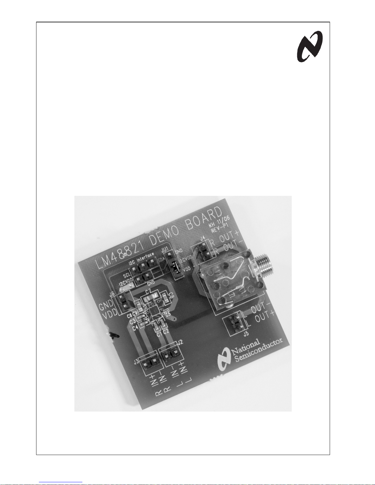
To help the user investigate and evaluate the LM48821's performance and capabilities, a fully populated demonstration
board is available from the National Semiconductor
Corporation's Audio Products Group. This board is shown in
Figure 1. Connected to an external power supply (2.0V to
4.0V), a signal source and an I2C controller (or signal source),
the LM48821 demonstration board easily demonstrate the
amplifier's features.
30009811
FIGURE 1. The LM48821 Demonstration Board
© 2007 National Semiconductor Corporation 300098 www.national.com
LM48821 Evaluation Board User's Guide AN-1589
General Description
The LM48821 is a fully differential input stereo headphone
audio amplifier with an internal digitally controlled volume
control. The LM48821 is optimized to operate over a power
supply voltage range of 2.0V to 4.0V. This amplifier is capable
of delivering 53mW
RMS
per channel into a 32Ω load at 1%
THD when powered by a 3.0V power supply.
Boomer audio power amplifiers were designed specifically to
provide high quality output power with a minimal amount of
external components. To that end, the LM48821 features two
functions that optimize system cost and minimize PCB area:
an integrated, digitally controlled (I2C bus) volume control and
an amplifier generated negative power supply voltage that
eliminates output signal-coupling capacitors. Since the
LM48821 does not require bootstrap capacitors, snubber networks, or output coupling capacitors, it is optimally suited for
low-power, battery powered potable systems.
The LM48821 includes separate shutdown controls for each
stereo channel for micropower dissipation, an internal thermal
shutdown protection mechanism, and is unity gain stable.
Operating Conditions
■ Temperature Range –40°C ≤ T
A
≤ 85°C
■ Amplifier Power
Supply Voltage
2.0V ≤ VDD ≤ 5.0V ≤ 4.0V
Board Features
The LM48821 demonstration board has all of the necessary
connections, using 0.100” headers, to apply the power supply
voltage, the audio input signals, and the I2C signal inputs. The
amplified audio signal is available on both a stereo headphone jack and auxiliary output connections.
Also included with the demonstration board is an I2C signal
generation board and software. With this board and the software, the user can easily control the LM48821’s, shutdown
function, mute, and stereo volume control. Figure 3 shows the
software’s graphical user interface.
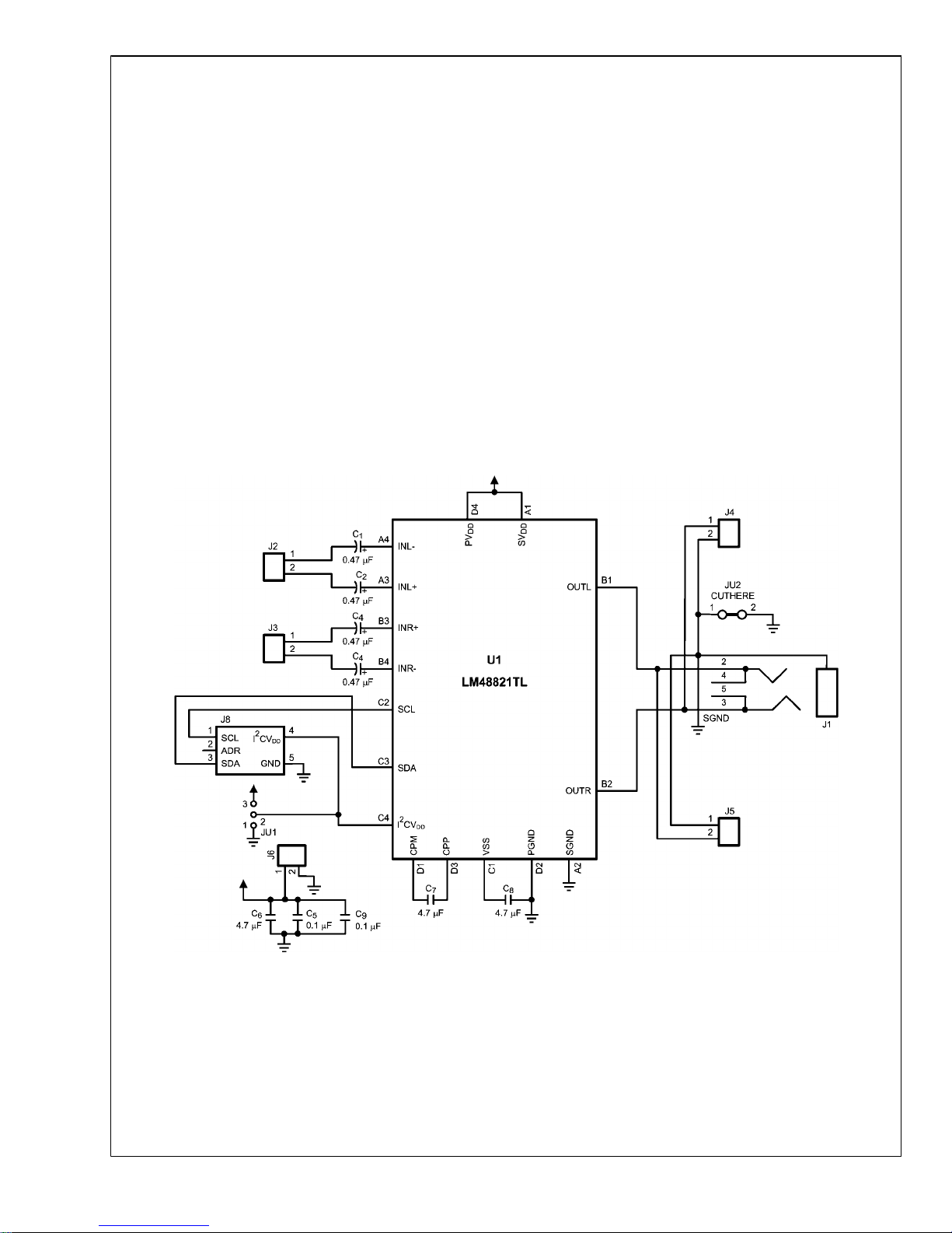
Schematic
Figure 2 shows the LM48821 Demonstration Board schematic. Refer to Table 3 for a list of the connections and their
functions.
30009846
Figure 2. The LM48821 Demonstration Board Schematic
www.national.com 2
AN-1589
Connections
Connecting to the world is accomplished through the 0.100”
headers on the LM48821 demonstration board. The functions
of the different headers are detailed in Table 1.
TABLE 1. LM48821 Demonstration Board Connections
Jumper Designation Function or Use
J1 Stereo, 0.125” headphone jack. Left channel is on the tip connector
and the right channel is on the ring connector. Ground is on the sleeve
connector.
J2 This is the connection to the amplifier’s differential left channel input.
Apply an external differential signal source’s positive voltage to the J2
pin labeled “L IN+” and the signal source’s negative input to the pin
labeled “L IN-.”
J3 This is the connection to the amplifier’s differential right channel input.
Apply an external differential signal source’s positive voltage to the J3
pin labeled “R IN+” and the signal source’s negative input to the pin
labeled “R IN-.”
J4 This is the connection to the amplifier’s single-ended, ground-
referenced right channel output. Connect the J4 pin labeled “R OUT
+” and the pin labeled “R OUT-” to the positive and ground inputs,
respectively, of an external signal measurement device. J4’s pin
labeled “R OUT+” corresponds to the headphone jack’s “ring”
connection. J4’s pin labeled “R OUT-“ corresponds to the headphone
jack’s “sleeve” (or ground) connection.
J5 This is the connection to the amplifier’s single-ended, ground-
referenced left channel output. Connect the J5 pin labeled “L OUT+”
and the pin labeled “L OUT-” to the positive and ground inputs,
respectively, of an external signal measurement device. J5’s pin
labeled “L OUT+” corresponds to the headphone jack’s “tip”
connection. J5’s pin labeled “L OUT-“ corresponds to the headphone
jack’s “sleeve” (or ground) connection.
J6 Power supply connection. Connect an external power supply’s
positive voltage source (2.0V to 4.0V) to the J6 pin labeled “VDD” and
the supply’s ground source to the pin labeled “GND.”
J8 (I2C Interface) This is the input connection for the I2C serial clock and serial data
signals. J8-pin 1 is for the SCL signal, JP8-pin 2 is not used. J8-pin 3
is for the SDA signal. J8-pin 4 is for an I2C VDD supply voltage supplied
by the I2C signal source. J8-pin 5 is for ground.
JU1 If an external I2C power supply voltage is used, connect this supply’s
positive voltage source to the JU1 pin labeled “I2CVDD” and the
supply’s ground source to the pin labeled “GND.” If the external V
DD
power supply is used for the I2CVDDvoltage, place a jumper between
the JU1 pin labeled “VDD” and the JU1 pin labeled “I2CVDD.”
3 www.national.com
AN-1589
Power Supply Sequencing
The LM48821 uses two power supply voltages: VDD for the
analog circuitry and I2CVDD, which defines the digital control
logic high voltage level. To ensure proper functionality, apply
VDD first, followed by I2CVDD. If one power supply is used,
VDD and I2CVDD can be connected together. The part will
power-up with both channels shutdown, the volume control
set to minimum, and the mute function active.
I2C Signal Generation Board and
Software
The I2C signal generation and interface board, along with the
LM48821 software, will generate the address byte and the
data byte used in the I2C control data transaction. To use the
I2C signal generation and interface board, please plug it into
a PC’s parallel port (on either a notebook or a desktop computer).
The software comes with an installer. To install, unzip the file
titled “LM48821_Software.” After the file unzips, double-click
the “setup.exe” file. After it launches, please follow the
installer’s instructions. Setup will create a folder named
“LM48821” in the “Program” folder on the “C” disk (if the default is used) along with a shortcut of the same name in the
“Programs” folder in the “Start” menu.
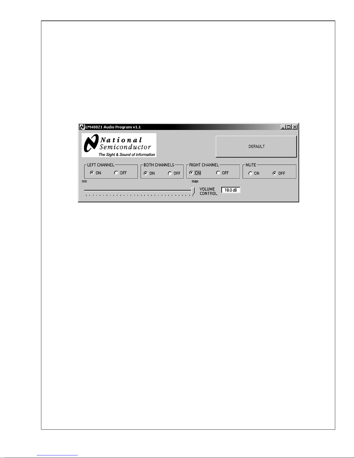
30009810
Figure 3. The LM48821 Software User's Interface
The LM48821 program includes controls for the amplifier’s
volume control, individual channel shutdown, and the mute
function. The control program's on-screen user interface is
shown in Figure 3.
The Default button is used to return the LM48821 to its poweron reset state: minimum volume setting, shutdown on both
amplifiers active, and mute active.
The LM48821’s stereo VOLUME CONTROL has 32 steps
and a gain range of –76dB to 18dB. It is controlled using the
slider located at the bottom of the program’s window. Each
time the slider is moved from one tick mark to another, the
program updates the amplifier’s volume control.
LEFT CHANNEL, BOTH CHANNELS, and RIGHT CHANNEL controls each have two buttons. For the left and right
channel control, the “ON” button activates its respective channel, whereas the “OFF” button places its respective channel
in shutdown mode. Selecting the BOTH CHANNELS “ON”
button simultaneously activates both channels, whereas selecting the “OFF” button places channels in shutdown mode.
PCB Layout Guidelines
This section provides general practical guidelines for PCB
layouts that use various power and ground traces. Designers
should note that these are only "rule-of-thumb" recommendations and the actual results are predicated on the final
layout.
POWER AND GROUND CIRCUITS
Star trace routing techniques (returning individual traces back
to a central point rather than daisy chaining traces together in
a serial manner) can have a major positive impact on low-level
signal performance. Star trace routing refers to using individual traces that radiate from a signal point to feed power and
ground to each circuit or even device. This technique may
require greater design time, but should not increase the final
price of the board.
For good THD+N and low noise performance and to ensure
correct power-on behavior at the maximum allowed supply
voltage, a local 4.7μF power supply bypass capacitor should
be connected as physically close as possible to the PVDD pin.
AVOIDING TYPICAL DESIGN/LAYOUT PROBLEMS
Avoid ground loops or running digital and analog traces parallel to each other (side-by-side) on the same PCB layer.
When traces must cross over each other, do so at 90 degrees.
Running digital and analog traces at 90 degrees to each other
from the top to the bottom side as much as possible will minimize capacitive noise coupling and crosstalk.
www.national.com 4
AN-1589
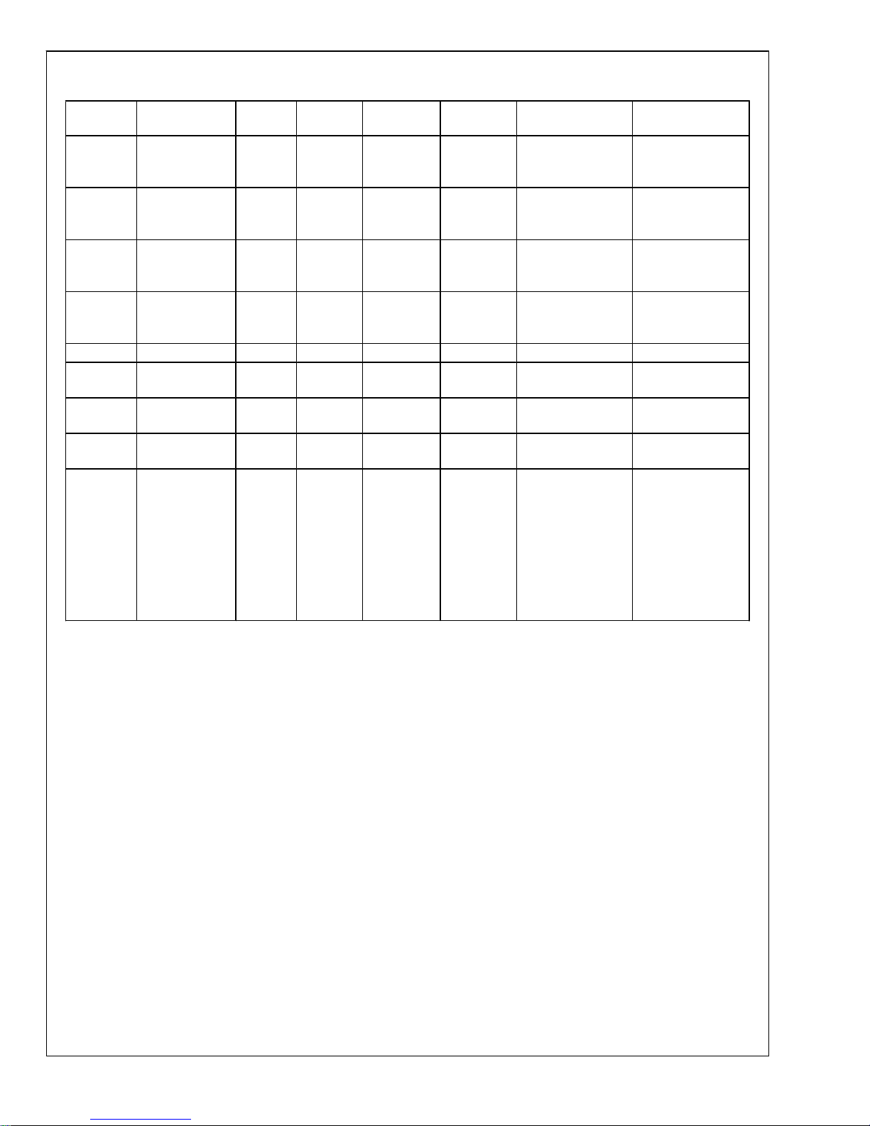
Bill of Materials
Designator Part Description Value Tolerance Rating Package
Type
Manufacturer Manufacturer's
Part Number
C1–C4
TACmicrochip
tantalum
capacitor
0.47μF
±20% 10V 0402 AVX TACK474M010PTA
C5, C9
Multilayer
Ceramic
Capacitor
0.1μF
±10% 6.3V 0201 TDK C0603X5R1A104M
C6, C8
Multilayer
Ceramic
Capacitor
4.7μF
±20% 6.3V 0603 TDK C1608X5R1A475M
C7
Multilayer
Ceramic
Capacitor
4.7μF
±20% 10V 0805 TDK C2012X5R1A475M
J1 Headphone Jack
J2–J6
2-pin header,
100mil lead pitch
J8
5-pin header,
100mil lead pitch
JU1
3-pin header,
100mil lead pitch
U1
LM48821Direct
Coupled TruGND, Ultra Low
Noise, 80mW
Differential
Inputs Stereo
Headphone
Amplifier with I2C
Volume Control
National
Semiconductor Corp
LM48821TL
5 www.national.com
AN-1589
 Loading...