

National Semiconductor LM4861 Technical data
LM4861
1.1W Audio Power Amplifier with Shutdown Mode
LM4861 1.1W Audio Power Amplifier with Shutdown Mode
February 2003
General Description
The LM4861 is a bridge-connected audio power amplifier
capable of delivering 1.1W of continuous average power to
an 8Ω load with 1% THD+N using a 5V power supply.
Boomer audio power amplifiers were designed specifically to
provide high quality output power with a minimal amount of
external components using surface mount packaging. Since
the LM4861 does not require output coupling capacitors,
bootstrap capacitors, or snubber networks, it is optimally
suited for low-power portable systems.
The LM4861 features an externally controlled, low-power
consumption shutdown mode, as well as an internal thermal
shutdown protection mechanism.
The unity-gain stable LM4861 can be configured by external
gain-setting resistors for differential gains of up to 10 without
the use of external compensation components. Higher gains
may be achieved with suitable compensation.
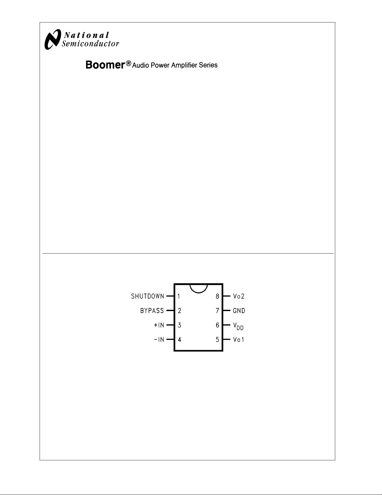
Connection Diagram
Key Specifications
j
THD+N for 1kHz at 1W continuous
average output power into 8Ω 1.0% (max)
j
Output power at 10% THD+N
at 1kHz into 8Ω
j
Shutdown Current 0.6µA (typ)
1.5W (typ)
Features
n No output coupling capacitors, bootstrap capacitors, or
snubber circuits are necessary
n Small Outline (SO) packaging
n Compatible with PC power supplies
n Thermal shutdown protection circuitry
n Unity-gain stable
n External gain configuration capability
Applications
n Personal computers
n Portable consumer products
n Self-powered speakers
n Toys and games
See NS Package Number M08A
Boomer®is a registered trademark of National Semiconductor Corporation.
Small Outline Package
01198602
Top View
Order Number LM4861M
© 2003 National Semiconductor Corporation DS011986 www.national.com
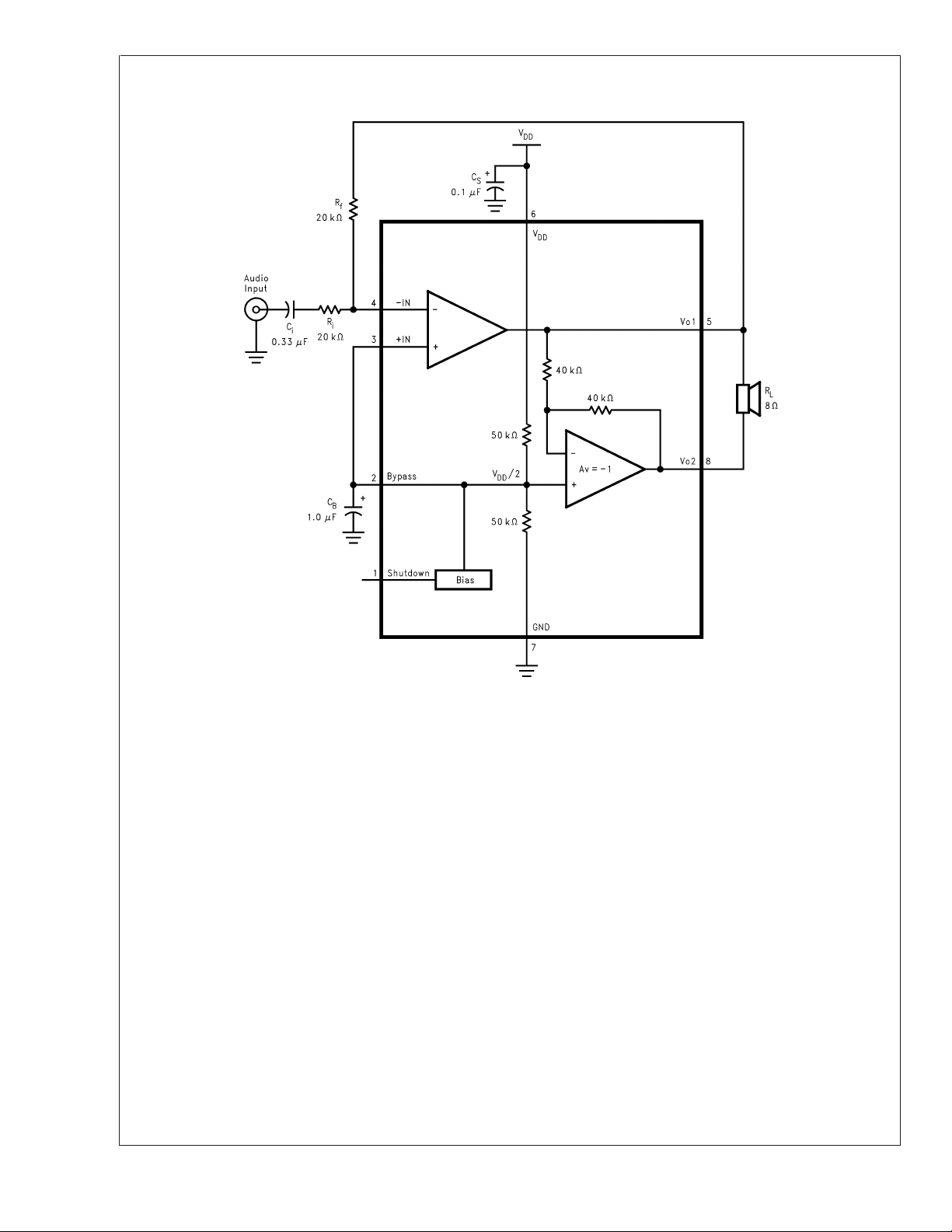
Typical Application
LM4861
FIGURE 1. Typical Audio Amplifier Application Circuit
01198601
www.national.com 2

LM4861
Absolute Maximum Ratings (Note 2)
If Military/Aerospace specified devices are required,
please contact the National Semiconductor Sales Office/
See AN-450 “Surface Mounting and their Effects on
Product Reliability” for other methods of soldering surface
mount devices.
Distributors for availability and specifications.
Supply Voltage 6.0V
Storage Temperature −65˚C to +150˚C
Input Voltage −0.3V to V
DD
0.3V
Power Dissipation (Note 3) Internally limited
ESD Susceptibility (Note 4) 3000V
ESD Susceptibility (Note 5) 250V
Junction Temperature 150˚C
Soldering Information
Small Outline Package
Vapor Phase (60 sec.)
Infrared (15 sec.)
215˚C
220˚C
+
Operating Ratings
Temperature Range
T
≤ TA≤ T
MIN
Supply Voltage 2.0V ≤ V
Thermal Resistance
θ
(typ) —M08A 35˚C/W
JC
θ
(typ) — M08A 140˚C/W
JA
θ
(typ) — N08E 37˚C/W
JC
θ
(typ) — N08E 107˚C/W
JA
MAX
−40˚C ≤ TA≤
+85˚C
≤ 5.5V
DD
Electrical Characteristics (Note 1) (Note 2)
The following specifications apply for VDD= 5V, unless otherwise specified. Limits apply for TA= 25˚C.
LM4861
Symbol Parameter Conditions
Typical Limit
(Note 6) (Note 7)
V
DD
Supply Voltage 2.0 V (min)
5.5 V (max)
I
DD
I
SD
V
OS
P
O
THD+N Total Harmonic Distortion + Noise P
PSRR Power Supply Rejection Ratio V
Note 1: All voltages are measured with respect to the ground pin, unless otherwise specified.
Note 2: Absolute Maximum Ratings indicate limits beyond which damage to the device may occur. Operating Ratings indicate conditions for which the device is
functional, but do not guarantee specific performance limits. Electrical Characteristics state DC and AC electrical specifications under particular test conditions which
guarantee specific performance limits. This assumes that the device is within the Operating Ratings. Specifications are not guaranteed for parameters where no limit
is given, however, the typical value is a good indication of device performance.
Note 3: The maximum power dissipation must be derated at elevated temperatures and is dictated by T
allowable power dissipation is P
and the typical junction-to-ambient thermal resistance, when board mounted, is 140˚C/W.
Note 4: Human body model, 100pF discharged through a 1.5kΩ resistor.
Note 5: Machine Model, 220pF– 240pF discharged through all pins.
Note 6: Typicals are measured at 25˚C and represent the parametric norm.
Note 7: Limits are guaranteed to Nationai’s AOQL (Average Outgoing Quality Level).
Note 8: The quiescent power supply current depends on the offset voltage when a practical load is connected to the amplifier.
Quiescent Power Supply Current VIN= 0V, IO= 0A (Note 8) 6.5 10.0 mA (max)
Shutdown Current V
pin1=VDD
0.6 10.0 µA (max)
Output Offset Voltage VIN= 0V 5.0 50.0 mV (max)
Output Power THD = 1% (max);f=1kHz 1.1 1.0 W(min)
= 1Wrms; 20 Hz ≤ f ≤ 20 kHz 0.72 %
O
= 4.9V to 5.1V 65 dB
DD
, θJA, and the ambient temperature TA. The maximum
DMAX
=(T
)/θJAor the number given in theAbsolute Maximum Ratings, whichever is lower. For the LM4861, T
JMAX−TA
JMAX
Units
(Limits)
= 150˚C,
JMAX
www.national.com3
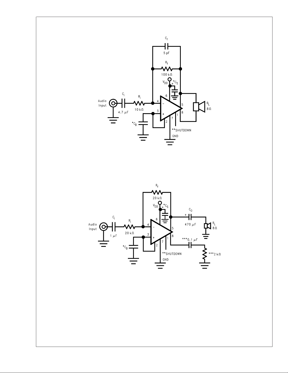
High Gain Application Circuit
LM4861
01198603
FIGURE 2. Audio Ampiifier with AVD=20
Single Ended Application Circuit
*CSand CBsize depend on specific application requirements and constraints. Typical vaiues of CSand CBare 0.1 µF.
**Pin 1 should be connected to V
***These components create a “dummy” load for pin 8 for stability purposes.
to disable the amplifier or to GND to enable the amplifier. This pin should not be left floating.
DD
FIGURE 3. Single-Ended Amplifier with AV=−1
01198604
www.national.com 4
 Loading...