

September 2007
LM48511
3W, Ultra-Low EMI, Filterless, Mono, Class D Audio Power
Amplifier with Spread Spectrum
General Description
The LM48511 integrates a boost converter with a high efficiency Class D audio power amplifier to provide 3W continuous power into an 8Ω speaker when operating from a 5V
power supply. When operating from a 3V to 4V power supply,
the LM48511 can be configured to drive 1 to 2.5W into an
8Ω load with less than 1% distortion (THD+N). The Class D
amplifier features a low noise PWM architecture that eliminates the output filter, reducing external component count,
board area consumption, system cost, and simplifying design.
A selectable spread spectrum modulation scheme suppresses RF emissions, further reducing the need for output filters.
The LM48511’s switching regulator is a current-mode boost
converter operating at a fixed frequency of 1MHz. Two selectable feedback networks allow the LM48511 regulator to
dynamically switch between two different output voltages, improving efficiency by optimizing the amplifier’s supply voltage
based on battery voltage and output power requirements.
The LM48511 is designed for use in portable devices, such
as GPS, mobile phones, and MP3 players. The high, 80%
efficiency at 5V, extends battery life when compared to Boosted Class AB amplifiers. Independent regulator and amplifier
shutdown controls optimize power savings by disabling the
regulator when high output power is not required.
The gain of the LM48511 is set by external resistors, which
allows independent gain control from multiple sources by
summing the signals. Output short circuit and thermal overload protection prevent the device from damage during fault
conditions. Superior click and pop suppression eliminates audible transients during power-up and shutdown.
Key Specifications
■ Quiescent Power Supply Current
VDD = 3V
VDD = 5V
9mA (typ)
13.5mA (typ)
■ P
O
at VDD = 5V, PV1 = 7.8V
RL = 8Ω, THD+N = 1%
3.0W (typ)
■ P
O
at VDD = 3V, PV1 = 4.8V
RL = 8Ω, THD+N = 1%
1W (typ)
■ Shutdown Current at V
DD
= 3V
0.01μA (typ)
Features
■
3W Output into 8Ω at 5V with THD+N = 1%
■
Selectable spread spectrum mode reduces EMI
■
80% Efficiency
■
Independent Regulator and Amplifier Shutdown Controls
■
Dynamically Selectable Regulator Output Voltages
■
Filterless Class D
■
3.0V – 5.5V operation
■
Low Shutdown Current
■
Click and Pop Suppression
Applications
■
GPS
■
Portable media
■
Cameras
■
Mobile Phones
■
Handheld games
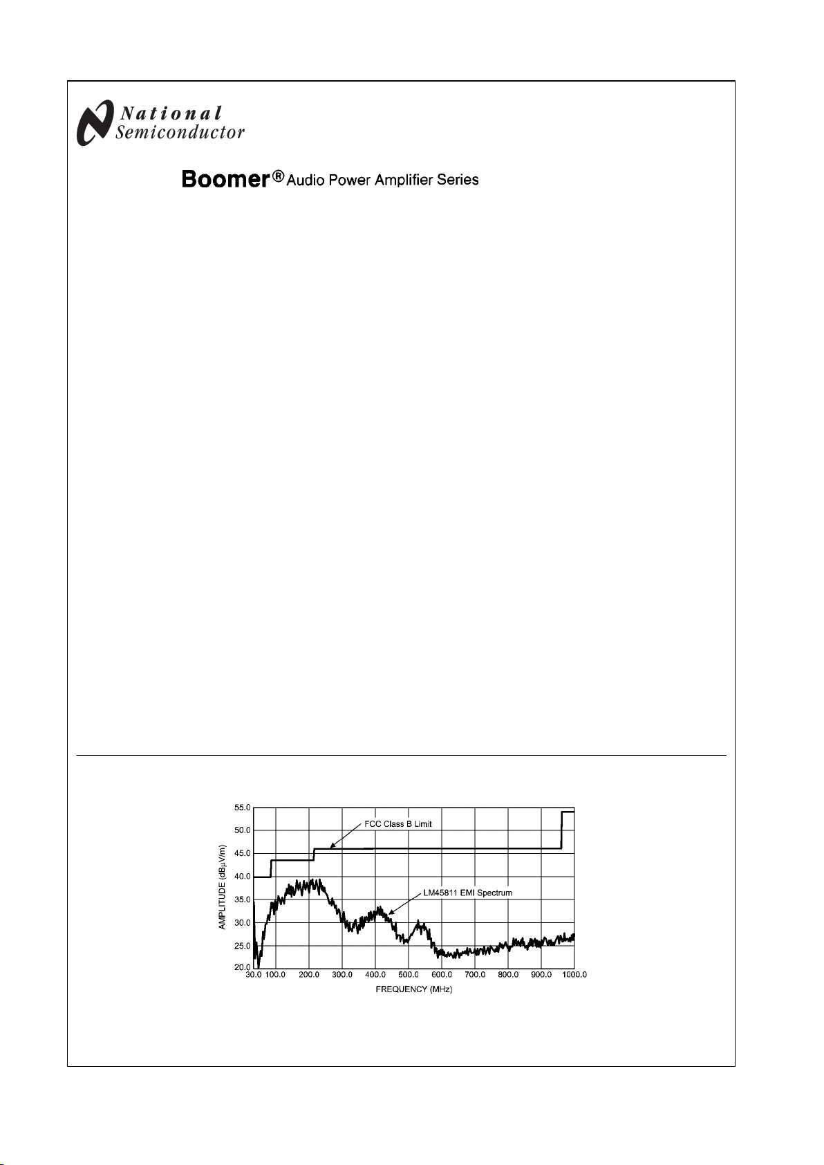
EMI Graph
300222h5
FIGURE 1. LM48511 RF Emissions — 3 inch cable
Boomer® is a registered trademark of National Semiconductor Corporation.
© 2007 National Semiconductor Corporation 300222 www.national.com
LM48511 3W, Ultra-Low EMI, Filterless, Mono, Class D Audio Power Amplifier
with Spread Spectrum
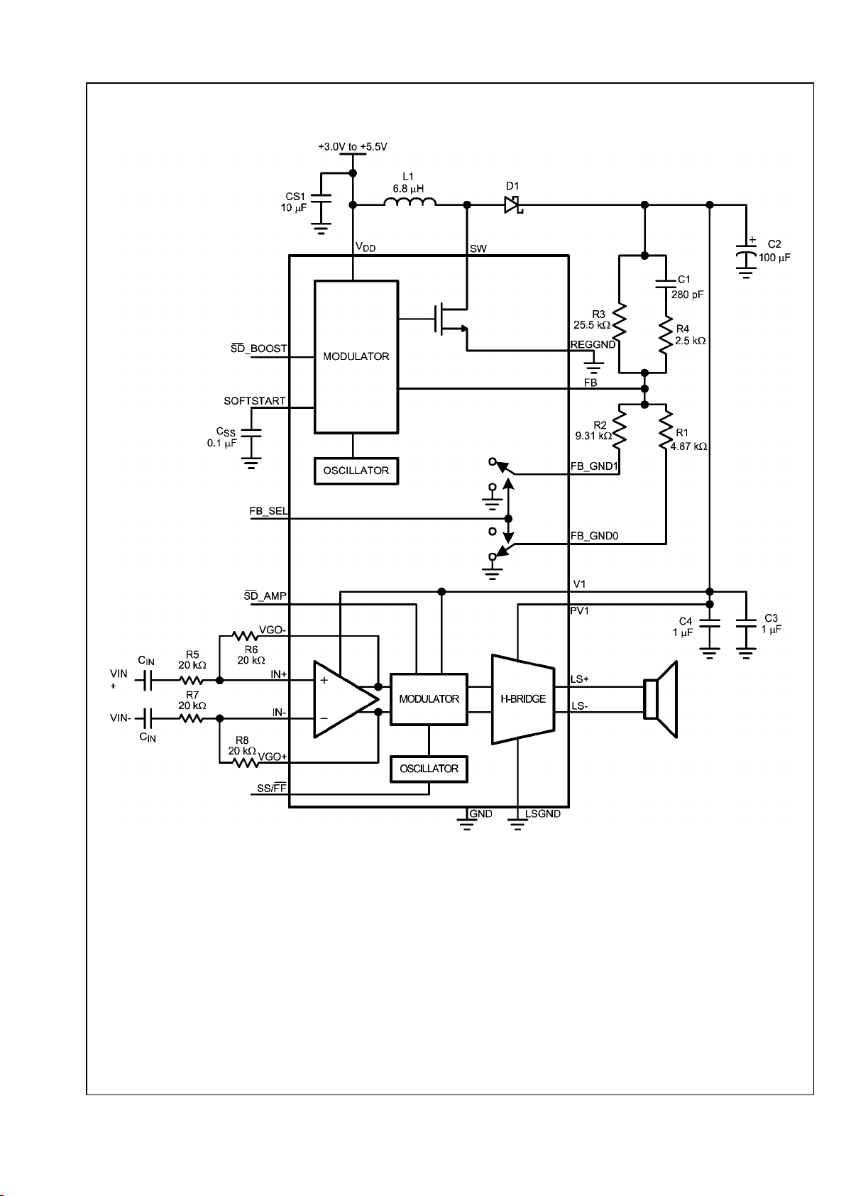
Typical Application
300222i3
FIGURE 2. Typical LM48511 Audio Amplifier Application Circuit
www.national.com 2
LM48511
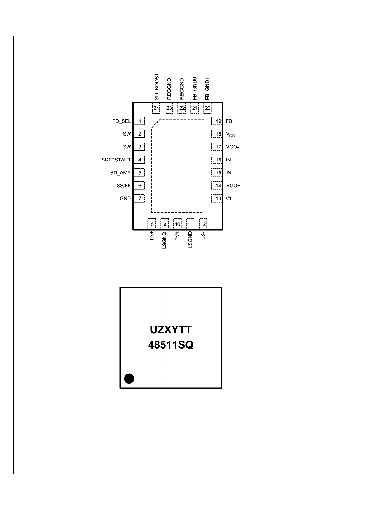
Connection Diagrams
SQ Package
300222d4
Top View
Order Number LM48511SQ
See NS Package Number SQA24B
SQ Package Marking
300222d5
Top View
U — Wafer fab code
Z — Assembly plant
XY — 2 Digit date code
TT — Lot traceability
3 www.national.com
LM48511
Pin Descriptions
LLP-24 Pin Name Function
1 FB_SEL
Regulator Feedback Select. Connect to VDD to select feedback
network connected to FB_GND1. Connect to GND to select
feedback network connected to FB_GND0.
2,3 SW Drain of the Internal FET Switch
4 SOFTSTART Soft Start Capacitor
5 SD_AMP
Amplifier Active Low Shutdown. Connect to VDD for normal
operation. Connect to GND to disable amplifier.
6 SS/FF
Modulation Mode Select. Connect to VDD for spread spectrum
mode (SS). Connect to GND for fixed frequency mode (FF).
7 GND Signal Ground
8 LS+ Amplifier Non-Inverting Output
9, 11 LSGND Amplifier H-Bridge Ground
10 PV1 Amplifier H-Bridge Power Supply. Connect to V1.
12 LS- Amplifier Inverting Output
13 V1 Amplifier Supply Voltage. Connect to PV1
14 VG0+ Amplifier Non-Inverting Gain Output
15 IN- Amplifier Inverting Input
16 IN+ Amplifier Non-Inverting Input
17 VG0– Amplifier Inverting Gain Output
18 VDD Power Supply
19 FB
Regulator Feedback Input. Connect FB to an external resistive
voltage divider to set the boost output voltage.
20 FB_GND1 Ground return for R3, R1 resistor divider
21 FB_GND0 Ground return for R3, R2 resistor divider
22,23 REGGND Power Ground (Booster)
24 SD_BOOST
Regulator Active Low Shutdown. Connect to VDD for normal
operation. Connect to GND to disable regulator.
DAP
To be soldered to board for enhanced thermal dissipation. Connect
to GND plane.
www.national.com 4
LM48511
Absolute Maximum Ratings (Notes 2, 2)
If Military/Aerospace specified devices are required,
please contact the National Semiconductor Sales Office/
Distributors for availability and specifications.
Supply Voltage (VDD, PV1, V1)
9V
Storage Temperature −65°C to +150°C
Input Voltage
−0.3V to VDD + 0.3V
Power Dissipation (Note 3) Internally limited
ESD Susceptibility (Note 4) 2000V
ESD Susceptibility (Note 5) 200V
Junction Temperature 150°C
Thermal Resistance
θJC (SQ)
3.8°C/W
θJA (SQ)
32.8°C/W
Operating Ratings
Temperature Range
T
MIN
≤ TA ≤ T
MAX
−40°C ≤ TA ≤ +85°C
Supply Voltage (VDD) 3.0V ≤ VDD ≤ 5.5V
Amplifier Voltage (PV1, V1) 4.8V ≤ PV1 ≤ 8.0V
Electrical Characteristics VDD = 5.0V (Notes 1, 2, 11)
The following specifications apply for VDD = 5.0V, PV1 = 7.8V (continuos mode), AV = 2V/V, R3 = 25.5kΩ, RLS = 4.87kΩ, RL =
8Ω, f = 1kHz, SS/FF = GND, unless otherwise specified. Limits apply for TA = 25°C.
Symbol Parameter Conditions
LM48511 Units
(Limits)
Typical
(Note 6)
Limit
(Notes 7, 8)
I
DD
Quiescent Power Supply Current
VIN = 0, R
LOAD
= ∞
Fixed Frequency Mode (FF) 13.5 mA (max)
Spread Spectrum Mode (SS) 14.5 22 mA (max)
I
SD
Shutdown Current
V
SD_BOOST
= V
SD_AMP
= SS =
FB_SEL = GND
0.11 1
μA (max)
V
IH
Logic Voltage Input High
1.03 1.4 V (min)
V
IL
Logic Voltage Input Low
0.92 0.4 V (min)
T
WU
Wake-up Time
CSS = 0.1μF
49 ms
V
OS
Output Offset Voltage Note 12 0.01 3 mV
P
O
Output Power
RL = 8Ω
f = 1kHz, BW = 22kHz
THD+N = 1%
FF
SS
3.0
3.0
2.6 W (min)
W
THD+N = 10%
FF
SS
3.8
3.8
W
W
RL = 4Ω
f = 1kHz, BW = 22kHz
THD+N = 1%
FF
SS
5.4
5.4
W
W
THD+N = 10%
FF
SS
6.7
6.7
W
W
THD+N Total Harmonic Distortion + Noise
PO = 2W, f = 1kHz, RL = 8Ω
FF
SS
0.03
0.03
%
%
PO = 3W, f = 1kHz, RL = 4Ω
FF
SS
0.04
0.05
%
%
5 www.national.com
LM48511
Symbol Parameter Conditions
LM48511 Units
(Limits)
Typical
(Note 6)
Limit
(Notes 7, 8)
ε
OS
Output Noise
f = 20Hz to 20kHz
Inputs to AC GND, No weighting
FF
SS
32
32
µV
RMS
µV
RMS
f = 20Hz to 20kHz
Inputs to AC GND, A weighted
FF
SS
22
22
µV
RMS
µV
RMS
PSRR
Power Supply Rejection Ratio
(Input Referred)
V
RIPPLE
= 200mV
P-P
Sine,
f
RIPPLE =
= 217Hz,
FF
SS
88
87
dB
dB
V
RIPPLE
= 200mV
P-P
Sine,
f
RIPPLE =
= 1kHz,
FF
SS
88
85
dB
dB
V
RIPPLE
= 200mV
P-P
Sine,
f
RIPPLE =
= 10kHz,
FF
SS
77
76
dB
dB
CMRR
Common Mode Rejection Ratio
(Input Referred)
V
RIPPLE
= 1V
P-P
, f
RIPPLE
= 217Hz
73
dB
η
Efficiency
f = 1kHz, RL = 8Ω, PO = 1W
80
%
V
FB
Feedback Pin Reference Voltage 1.23
V
Electrical Characteristics VDD = 3.6V (Notes 1, 2, 11)
The following specifications apply for VDD = 3.6V, PV1 = 7V (continuous mode), AV = 2V/V, R3 = 25.5kΩ, RLS = 5.36kΩ, RL = 8Ω,
f = 1kHz, SS/FF
= GND, unless otherwise specified. Limits apply for TA = 25°C.
Symbol Parameter Conditions
LM48511 Units
(Limits)
Typical
(Note 6)
Limit
(Notes 7, 8)
I
DD
Quiescent Power Supply Current
VIN = 0, R
LOAD
= ∞
Fixed Frequency Mode (FF) 16 mA (max)
Spread Spectrum Mode (SS) 17.5 26.6 mA (max)
I
SD
Shutdown Current
V
SD_BOOST
= V
SD_AMP
= SS =
FB_SEL = GND
0.03 1
μA (max)
V
IH
Logic Voltage Input High
0.96 1.4 V (min)
V
IL
Logic Voltage Input Low
0.84 0.4 V (min)
T
WU
Wake-up Time
CSS = 0.1μF
50 ms
V
OS
Output Offset Voltage Note 12 0.04 mV
www.national.com 6
LM48511
Symbol Parameter Conditions
LM48511 Units
(Limits)
Typical
(Note 6)
Limit
(Notes 7, 8)
P
O
Output Power
RL = 8Ω, f = 1kHz, BW = 22kHz
THD+N = 1%
FF
SS
2.5
2.5
W
W
THD+N = 10%
FF
SS
3.0
3.0
W
W
RL = 4Ω, f = 1kHz, BW = 22kHz
THD+N = 1%
FF
SS
4.3
4.2
W
W
THD+N = 10%
FF
SS
5.4
5.3
W
W
THD+N Total Harmonic Distortion + Noise
PO = 1.5W, f = 1kHz, RL = 8Ω
FF
SS
0.03
0.03
%
%
PO = 3W, f = 1kHz, RL = 4Ω
FF
SS
0.04
0.05
%
%
ε
OS
Output Noise
f = 20Hz to 20kHz
Inputs to AC GND, No weighting
FF
SS
35
36
µV
RMS
µV
RMS
f = 20Hz to 20kHz
Inputs to AC GND, A weighted
FF
SS
25
26
µV
RMS
µV
RMS
PSRR
Power Supply Rejection Ratio
(Input Referred)
V
RIPPLE
= 200mV
P-P
Sine,
f
RIPPLE =
= 217Hz
FF
SS
85
86
dB
dB
V
RIPPLE
= 200mV
P-P
Sine,
f
RIPPLE =
= 1kHz
FF
SS
87
86
dB
dB
V
RIPPLE
= 200mV
P-P
Sine,
f
RIPPLE =
= 10kHz
FF
SS
78
77
dB
dB
CMRR
Common Mode Rejection Ratio
(Input Referred)
V
RIPPLE
= 1V
P-P
, f
RIPPLE
= 217Hz
73
dB
η
Efficiency
f = 1kHz, RL = 8Ω, PO = 1W
77
%
V
FB
Feedback Pin Reference Voltage 1.23
V
7 www.national.com
LM48511

Electrical Characteristics VDD = 3.0V (Notes 1, 2, 11)
The following specifications apply for VDD = 3.0V, PV1 = 4.8V (continuos mode), AV = 2V/V, R3 = 25.5kΩ, RLS = 9.31kΩ, RL =
8Ω, f = 1kHz, SS/FF = GND, unless otherwise specified. Limits apply for TA = 25°C.
Symbol Parameter Conditions
LM48511 Units
(Limits)
Typical
(Note 6)
Limit
(Notes 7, 8)
I
DD
Quiescent Power Supply Current
VIN = 0, R
LOAD
= ∞
Fixed Frequency Mode (FF) 9 mA (max)
Spread Spectrum Mode (SS) 9.5 mA (max)
I
SD
Shutdown Current
V
SD_BOOST
= V
SD_AMP
= SS =
FB_SEL = GND
0.01 1
μA
V
IH
Logic Voltage Input High
0.91 V (min)
V
IL
Logic Voltage Input Low
0.79 V
T
WU
Wake-up Time
CSS = 0.1μF
49 ms
V
OS
Output Offset Voltage Note 12 0.04 mV
P
O
Output Power
RL = 8Ω, f = 1kHz, BW = 22kHz
THD+N = 1%
FF
SS
1
1
0.84 W (min)
W
THD+N = 10%
FF
SS
1.3
1.3
W
W
RL = 4Ω, f = 1kHz, BW = 22kHz
THD+N = 1%
FF
SS
1.8
1.8
W
W
THD+N = 10%
FF
SS
2.2
2.2
W
W
THD+N Total Harmonic Distortion + Noise
PO = 500mW, f = 1kHz, RL = 8Ω
FF
SS
0.02
0.03
%
%
PO = 500mW, f = 1kHz, RL = 4Ω
FF
SS
0.04
0.06
%
%
ε
OS
Output Noise
f = 20Hz to 20kHz
Inputs to AC GND, No weighting
FF
SS
35
35
µV
RMS
µV
RMS
f = 20Hz to 20kHz
Inputs to AC GND, A weighted
FF
SS
25
25
µV
RMS
µV
RMS
www.national.com 8
LM48511

Symbol Parameter Conditions
LM48511 Units
(Limits)
Typical
(Note 6)
Limit
(Notes 7, 8)
PSRR
Power Supply Rejection Ratio
(Input Referred)
V
RIPPLE
= 200mV
P-P
Sine,
f
RIPPLE =
= 217Hz
FF
SS
89
89
dB
dB
V
RIPPLE
= 200mV
P-P
Sine,
f
RIPPLE =
= 1kHz
FF
SS
88
88
dB
dB
V
RIPPLE
= 200mV
P-P
Sine,
f
RIPPLE =
= 10kHz
FF
SS
78
78
dB
dB
CMRR
Common Mode Rejection Ratio
(Input Referred)
V
RIPPLE
= 1V
P-P
, f
RIPPLE
= 217Hz
71
dB
η
Efficiency
f = 1kHz, RL = 8Ω, PO = 1W
75
%
V
FB
Feedback Pin Reference Voltage 1.23
V
Note 1: All voltages are measured with respect to the GND pin, unless otherwise specified.
Note 2: Absolute Maximum Ratings indicate limits beyond which damage to the device may occur. Operating Ratings indicate conditions for which the device is
functional, but do not guarantee specific performance limits. Electrical Characteristics state DC and AC electrical specifications under particular test conditions
which guarantee specific performance limits. This assumes that the device is within the Operating Ratings. Specifications are not guaranteed for parameters
where no limit is given, however, the typical value is a good indication of device performance.
Note 3: The maximum power dissipation must be derated at elevated temperatures and is dictated by T
JMAX
, θJA, and the ambient temperature, TA. The maximum
allowable power dissipation is P
DMAX
= (T
JMAX
− TA) / θJA or the given in Absolute Maximum Ratings, whichever is lower.
Note 4: Human body model, 100pF discharged through a 1.5kΩ resistor.
Note 5: Machine Model, 220pF–240pF discharged through all pins.
Note 6: Typicals are measured at 25°C and represent the parametric norm.
Note 7: Limits are guaranteed to National's AOQL (Average Outgoing Quality Level).
Note 8: Datasheet min/max specification limits are guaranteed by design, test, or statistical analysis.
Note 9: Shutdown current is measured with components R1 and R2 removed.
Note 10: Feedback pin reference voltage is measured with the Audio Amplifier disconnected from the Boost converter (the Boost converter is unloaded).
Note 11: RL is a resistive load in series with two inductors to simulate an actual speaker load for RL = 8Ω, the load is 15μH+8Ω+15μH. For RL = 4Ω, the load is
15μH+4Ω+15μH.
Note 12: Offset voltage is determined by: (I
DD (with load)
— I
DD (no load)
) x RL.
9 www.national.com
LM48511

Typical Performance Characteristics
THD+N vs Frequency
VDD = 5V, RL = 8Ω
PO = 2W, filter = 22kHz, PV1 = 7.8V
300222g9
THD+N vs Frequency
VDD = 3.6V, RL = 8Ω
PO = 500mW, filter = 22kHz, PV1 = 4.8V
300222g7
THD+N vs Frequency
VDD = 3V, RL = 8Ω
PO = 1.5W, filter = 22kHz, PV1 = 7V
300222g8
THD+N vs Output Power
VDD = 5V, RL = 8Ω
PO = 1.5W, f = 1kHz, filter = 22kHz, PV1 = 7.8V
300222h4
THD+N vs Output Power
VDD = 3.6V, RL = 8Ω
f = 1kHz, filter = 22kHz, PV1 = 7V
300222h1
THD+N vs Output Power
VDD = 3V, RL = 8Ω
f = 1kHz, filter = 22kHz, PV1 = 4.8V
300222h3
www.national.com 10
LM48511

THD+N vs Output Power
VDD = 3V, 3.6V, 5V, RL = 8Ω
f = 1kHz, filter = 22kHz, R1 = 4.87kΩ, FF
300222i1
THD+N vs Output Power
VDD = 3.6V, RL = 8Ω
filter = 22kHz, PV1 = 7.8V, PV1 = 7V, PV1 = 4.8V, FF
300222i0
Boost Amplifier vs Output Power
VDD = 5V, RL = 8Ω
f = 1kHz, PV1 = 7.8V
300222f7
Boost Amplifier vs Output Power
VDD = 3.6V, RL = 8Ω
f = 1kHz, PV1 = 7V
300222f5
Boost Amplifier vs Output Power
VDD = 3V, RL = 8Ω
f = 1kHz, PV1 = 4.8V
300222f6
PSRR vs Frequency
VDD = 5V, RL = 8Ω
V
RIPPLE
= 200mVPP, PV1 = 7.8V
300222g3
11 www.national.com
LM48511

PSRR vs Frequency
VDD = 3.6V, RL = 8Ω
V
RIPPLE
= 200mVPP, PV1 = 7V
300222g1
PSRR vs Frequency
VDD = 3V, RL = 8Ω
V
RIPPLE
= 200mVPP, PV1 = 4.8V
300222g2
Supply Current vs Supply Voltage
PV1 = 7.8V
300222g6
Supply Current vs Supply Voltage
PV1 = 7V
300222g5
Supply Current vs Supply Voltage
PV1 = 4.8V
300222g4
Power Dissipation vs Output Power
VDD = 5V, RL = 8Ω
PV1 = 7.8V, FF
300222g0
www.national.com 12
LM48511

Power Dissipation vs Output Power
VDD = 3.6V, RL = 8Ω
PV1 = 7V, FF
300222f8
Power Dissipation vs Output Power
VDD = 3V, RL = 8Ω
PV1 = 4.8V, FF
300222f9
Boost Converter Efficiency vs I
LOAD(DC)
VDD = 5V, PV1 = 7.8V
300222h8
Boost Converter Efficiency vs I
LOAD(DC)
VDD = 3.6V, PV1 =7V
300222h6
Boost Converter Efficiency vs I
LOAD(DC)
VDD = 3V, PV1 = 4.8V
300222h7
13 www.national.com
LM48511

Application Information
GENERAL AMPLIFIER FUNCTION
The LM48511 features a Class D audio power amplifier that
utilizes a filterless modulation scheme, reducing external
component count, conserving board space and reducing system cost. The outputs of the device transition from PV1 to
GND with a 300kHz switching frequency. With no signal applied, the outputs (V
LS+
and V
LS-
) switch with a 50% duty
cycle, in phase, causing the two outputs to cancel. This cancellation results in no net voltage across the speaker, thus
there is no current to the load in the idle state.
With the input signal applied, the duty cycle (pulse width) of
the LM48511 outputs changes. For increasing output voltage,
the duty cycle of V
LS+
increases, while the duty cycle of V
LS-
decreases. For decreasing output voltages, the converse
occurs. The difference between the two pulse widths yields
the differential output voltage.
FIXED FREQUENCY
The LM48511 features two modulations schemes, a fixed frequency mode (FF) and a spread spectrum mode (SS). Select
the fixed frequency mode by setting SS/FF
= GND. In fixed
frequency mode, the amplifier outputs switch at a constant
300kHz. In fixed frequency mode, the output spectrum consists of the fundamental and its associated harmonics (see
Typical Performance Characteristics).
SPREAD SPECTRUM MODE
The logic selectable spread spectrum mode eliminates the
need for output filters, ferrite beads or chokes. In spread
spectrum mode, the switching frequency varies randomly by
10% about a 330kHz center frequency, reducing the wideband spectral contend, improving EMI emissions radiated by
the speaker and associated cables and traces. Where a fixed
frequency class D exhibits large amounts of spectral energy
at multiples of the switching frequency, the spread spectrum
architecture of the LM48511 spreads that energy over a larger
bandwidth (See Typical Performance Characteristics). The
cycle-to-cycle variation of the switching period does not affect
the audio reproduction, efficiency, or PSRR. Set SS/FF
=
VDD for spread spectrum mode.
DIFFERENTIAL AMPLIFIER EXPLANATION
The LM48511 includes fully differential amplifier that features
differential input and output stages. A differential amplifier
amplifies the difference between the two input signals. Traditional audio power amplifiers have typically offered only single-ended inputs resulting in a 6dB reduction in signal to noise
ratio relative to differential inputs. The LM48511 also offers
the possibility of DC input coupling which eliminates the two
external AC coupling, DC blocking capacitors. The LM48511
can be used, however, as a single ended input amplifier while
still retaining it's fully differential benefits. In fact, completely
unrelated signals may be placed on the input pins. The
LM48511 simply amplifies the difference between the signals.
A major benefit of a differential amplifier is the improved common mode rejection ratio (CMRR) over single input amplifiers.
The common-mode rejection characteristic of the differential
amplifier reduces sensitivity to ground offset related noise injection, especially important in high noise applications.
AUDIO AMPLIFIER POWER DISSIPATION AND
EFFICIENCY
The major benefit of a Class D amplifier is increased efficiency
versus a Class AB. The efficiency of the LM48511 is attributed
to the region of operation of the transistors in the output stage.
The Class D output stage acts as current steering switches,
consuming negligible amounts of power compared to their
Class AB counterparts. Most of the power loss associated
with the output stage is due to the IR loss of the MOSFET onresistance, along with switching losses due to gate charge.
REGULATOR POWER DISSIPATION
At higher duty cycles, the increased ON-time of the switch
FET means the maximum output current will be determined
by power dissipation within the LM48511 FET switch. The
switch power dissipation from ON-time conduction is calculated by:
P
D(SWITCH)
= DC x (I
INDUCTOR(AVE)
)2 x R
DS(ON)
(W) (1)
where DC is the duty cycle.
SHUTDOWN FUNCTION
The LM48511 features independent amplifier and regulator
shutdown controls, allowing each portion of the device to be
disabled or enabled independently. SD_AMP controls the
Class D amplifiers, while SD_BOOST controls the regulator.
Driving either inputs low disables the corresponding portion
of the device, and reducing supply current.
When the regulator is disabled, both FB_GND switches open,
further reducing shutdown current by eliminating the current
path to GND through the regulator feedback network. Without
the GND switches, the feedback resistors as shown in Figure
1 would consume an additional 165μA from a 5V supply. With
the regulator disabled, there is still a current path from VDD,
through the inductor and diode, to the amplifier power supply.
This allows the amplifier to operate even when the regulator
is disabled. The voltage at PV1 and V1 will be:
(VDD - [VD + (IL x DCR)] (2)
Where VD is the forward voltage of the Schottky diode, IL is
the current through the inductor, and DCR is the DC resistance of the inductor. Additionally, when the regulator is disabled, an external voltage between 5V and 8V can be applied
directly to PV1 and V1 to power the amplifier.
It is best to switch between ground and VDD for minimum current consumption while in shutdown. The LM48511 may be
disabled with shutdown voltages in between GND and VDD,
the idle current will be greater than the typical 0.1µA value.
Increased THD+N may also be observed when a voltage of
less than VDD is applied to SD_AMP .
REGULATOR FEEDBACK SELECT
The LM45811 regulator features two feedback paths as
shown in Figure 1, which allow the regulator to easily switch
between two different output voltages. The voltage divider
consists of the high side resistor, R3, and the low side resistors (RLS), R1 and R2. R3 is connected to the output of the
boost regulator, the mid-point of each divider is connected to
FB, and the low side resistors are connected to either
FB_GND1 or FB_GND0. FB_SEL determines which
FB_GND switch is closed, which in turn determines which
feedback path is used. For example if FB_SEL = VDD, the
FB_GND1 switch is closed, while the FB_GND0 switch remains open, creating a current path through the resistors
connected to FB_GND1. Conversely, if FB_SEL = GND, the
FB_GND0 switch is closed, while the FB_GND1 switch remains open, creating a current path through the resistors
connected to FB_GND0.
www.national.com 14
LM48511

FB_SEL can be susceptible to noise interference. To prevent
an accidental state change, either bypass FB_SEL with a
0.1µF capacitor to GND, or connect the higher voltage feedback network to FB_GND0, and the lower voltage feedback
network to FB_GND1. Because the higher output voltage
configuration typically generates more noise on VDD, this configuration minimizes the V
DD
noise exposure of FB_SEL, as
FB_SEL = GND for FB_GND0 (high voltage output) and
FB_SEL = VDD for FB_GND1 (low voltage output).
The selectable feedback networks maximize efficiency in two
ways. In applications where the system power supply voltage
changes, such as a mobile GPS receiver, that transitions from
battery power, to AC line, to a car power adapter, the
LM48511 can be configured to generate a lower voltage when
the system power supply voltages is lower, and conversely,
generate a higher voltage when the system power supply is
higher. See the Setting the Regulator Output Voltage (PV1)
section.
In applications where the same speaker/amplifier combination is used for different purposes with different audio power
requirements, such as a cell phone ear piece/speaker phone
speaker, the ability to quickly switch between two different
voltages allows for optimization of the amplifier power supply,
increasing overall system efficiency. When audio power demands are low (ear piece mode) the regulator output voltage
can be set lower, reducing quiescent current consumption.
When audio power demands increase (speaker phone
mode), a higher voltage increases the amplifier headroom,
increasing the audio power delivered to the speaker.
PROPER SELECTION OF EXTERNAL COMPONENTS
Proper selection of external components in applications using
integrated power amplifiers, and switching DC-DC converters, is critical for optimizing device and system performance.
Consideration to component values must be used to maximize overall system quality. The best capacitors for use with
the switching converter portion of the LM48511 are multi-layer
ceramic capacitors. They have the lowest ESR (equivalent
series resistance) and highest resonance frequency, which
makes them optimum for high frequency switching converters. When selecting a ceramic capacitor, only X5R and X7R
dielectric types should be used. Other types such as Z5U and
Y5F have such severe loss of capacitance due to effects of
temperature variation and applied voltage, they may provide
as little as 20% of rated capacitance in many typical applications. Always consult capacitor manufacturer’s data curves
before selecting a capacitor. High-quality ceramic capacitors
can be obtained from Taiyo-Yuden and Murata.
POWER SUPPLY BYPASSING
As with any amplifier, proper supply bypassing is critical for
low noise performance and high power supply rejection. The
capacitor location on both PV1, V1 and VDD pins should be
as close to the device as possible.
AUDIO AMPLIFIER GAIN SETTING RESISTOR
SELECTION
The amplifier gain of the LM48511 is set by four external resistors, the input resistors, R5 and R7, and the feed back
resistors R6 and R8.. The amplifier gain is given by:
Where RIN is the input resistor and RF is the feedback resistor.
AVD = 2 X RF / R
IN
(3)
Careful matching of the resistor pairs, R6 and R8, and R5 and
R7, is required for optimum performance. Any mismatch be-
tween the resistors results in a differential gain error that leads
to an increase in THD+N, decrease in PSRR and CMRR, as
well as an increase in output offset voltage. Resistors with a
tolerance of 1% or better are recommended.
The gain setting resistors should be placed as close to the
device as possible. Keeping the input traces close together
and of the same length increases noise rejection in noisy environments. Noise coupled onto the input traces which are
physically close to each other will be common mode and easily rejected.
AUDIO AMPLIFIER INPUT CAPACITOR SELECTION
Input capacitors may be required for some applications, or
when the audio source is single-ended. Input capacitors block
the DC component of the audio signal, eliminating any conflict
between the DC component of the audio source and the bias
voltage of the LM48511. The input capacitors create a highpass filter with the input resistors RIN. The -3dB point of the
high pass filter is found by:
f = 1 / 2πRINC
IN
(4)
In single-ended configurations, the input capacitor value affects click-and-pop performance. The LM48511 features a
50mg turn-on delaly. Choose the input capacitor / input resistor values such that the capacitor is charged before the
50ms turn-on delay expires. A capacitor value of 0.18μF and
a 20kΩ input resistor are recommended. In differential applications, the charging of the input capacitor does not affect
click-and-pop significantly.
The input capacitors can also be used to remove low frequency content from the audio signal. High pass filtering the
audio signal helps protect speakers that can not reproduce or
may be damaged by low frequencies. When the LM48511 is
using a single-ended source, power supply noise on the
ground is seen as an input signal. Setting the high-pass filter
point above the power supply noise frequencies, 217Hz in a
GSM phone, for example, filters out the noise such that it is
not amplified and heard on the output. Capacitors with a tolerance of 10% or better are recommended for impedance
matching and improved CMRR and PSRR.
SELECTING REGULATOR OUTPUT CAPACITOR
A single 100µF low ESR tantalum capacitor provides sufficient output capacitance for most applications. Higher capacitor values improve line regulation and transient response.
Typical electrolytic capacitors are not suitable for switching
converters that operate above 500kHz because of significant
ringing and temperature rise due to self-heating from ripple
current. An output capacitor with excessive ESR reduces
phase margin and causes instability.
SELECTING REGULATING BYPASS CAPACITOR
A supply bypass capacitor is required to serve as an energy
reservoir for the current which must flow into the coil each time
the switch turns on. This capacitor must have extremely low
ESR, so ceramic capacitors are the best choice. A nominal
value of 10μF is recommended, but larger values can be
used. Since this capacitor reduces the amount of voltage ripple seen at the input pin, it also reduces the amount of EMI
passed back along that line to other circuitry.
SELECTING THE SOFTSTART (CSS) CAPACITOR
The soft-start function charges the boost converter reference
voltage slowly. This allows the output of the boost converter
to ramp up slowly thus limiting the transient current at startup.
15 www.national.com
LM48511

Selecting a soft-start capacitor (CSS) value presents a trade
off between the wake-up time and the startup transient current. Using a larger capacitor value will increase wake-up time
and decrease startup transient current while the apposite effect happens with a smaller capacitor value. A general guideline is to use a capacitor value 1000 times smaller than the
output capacitance of the boost converter (C2). A 0.1uF softstart capacitor is recommended for a typical application.
The following table shows the relationship between CSS startup time and surge current.
C
SS
(μF)
Boost Set-up Time
(ms)
Input Surge Current
(mA)
0.1 5.1 330
0.22 10.5 255
0.47 21.7 220
VDD = 5V, PV1 = 7.8V (continuous mode)
SELECTING DIODE (D1)
Use a Schottkey diode, as shown in Figure 1. A 30V diode
such as the DFLS230LH from Diodes Incorporated is recommended. The DFLS230LH diodes are designed to handle a
maximum average current of 2A.
DUTY CYCLE
The maximum duty cycle of the boost converter determines
the maximum boost ratio of output-to-input voltage that the
converter can attain in continuous mode of operation. The
duty cycle for a given boost application is defined by:
Duty Cycle = (PV1+VD-VDD)/(PV1+VD-VSW) (5)
This applies for continuous mode operation.
SELECTING INDUCTOR VALUE
Inductor value involves trade-offs in performance. Larger inductors reduce inductor ripple current, which typically means
less output voltage ripple (for a given size of output capacitor).
Larger inductors also mean more load power can be delivered
because the energy stored during each switching cycle is:
E = L/2 x I
P
2
(6)
Where “lp” is the peak inductor current. The LM48511 will limit
its switch current based on peak current. With IP fixed, increasing L will increase the maximum amount of power available to the load. Conversely, using too little inductance may
limit the amount of load current which can be drawn from the
output. Best performance is usually obtained when the converter is operated in “continuous” mode at the load current
range of interest, typically giving better load regulation and
less output ripple. Continuous operation is defined as not allowing the inductor current to drop to zero during the cycle.
Boost converters shift over to discontinuous operation if the
load is reduced far enough, but a larger inductor stays continuous over a wider load current range.
INDUCTOR SUPPLIES
The recommended inductor for the LM48511 is the
IHLP-2525CZ-01 from Vishay Dale. When selecting an inductor, the continuous current rating must be high enough to
avoid saturation at peak currents. A suitable core type must
be used to minimize switching losses, and DCR losses must
be considered when selecting the current rating. Use shielded
inductors in systems that are susceptible to RF interference.
SETTING THE REGULATOR OUTPUT VOLTAGE (PV1)
The output voltage of the regulator is set through one of two
external resistive voltage-dividers (R3 in combination with either R1 or R2) connected to FB (Figure 1). The resistor, R4
is only for compensation purposes and does not affect the
regulator output voltage. The regulator output voltage is set
by the following equation:
PV1 = VFB [1+R3/RLS] (7)
Where V
FB
is 1.23V, and RLS is the low side resistor (R1 or
R2). To simplify resistor selection:
RLS = (R3VFB) / (PV1–VFB) (8)
A value of approximately 25.5kΩ is recommended for R3.
The quiescent current of the boost regulator is directly related
to the difference between its input and output voltages, the
larger the difference, the higher the quiescent current. For
improved power consumption the following regulator input/
output voltage combinations are recommended:
VDD (V)
PV1 (V)
R3(kΩ)
RLS (kΩ) P
OUT
into 8Ω (W)
3.0 4.8 25.5 9.31 1
3.6 7.1 25.5 5.35 2.5
5 7.8 25.5 4.87 3
The values of PV1 are for continuous mode operation.
For feedback path selection, see Regulator Feedback Select
section.
DISCONTINUOUS/CONTINUOUS OPERATION
The LM48511 regulator features two different switching
modes. Under light load conditions, the regulator operates in
a variable frequency, discontinuous, pulse skipping mode,
that improves light load efficiency by minimizing losses due
to MOSFET gate charge. Under heavy loads, the LM48511
regulator automatically switches to a continuous, fixed frequency PWM mode, improving load regulation. In discontinuous mode, the regulator output voltage is typically 400mV
higher than the expected (calculated) voltage in continuous
mode.
ISWFEED-FORWARD COMPENSATION FOR BOOST
CONVERTER
Although the LM48511 regulator is internally compensated,
an external feed-forward capacitor, (C1) may be required for
stability (Figure 1). The compensation capacitor places a zero
in regulator loop response. The recommended frequency of
the zero (fZ) is 22.2kHz. The value of C1 is given by:
C1 =1 / 2πR3f
Z
(9)
In addition to C1, a compensation resistor, R4 is required to
cancel the zero contributed by the ESR of the regulator output
capacitor. Calculate the zero frequency of the output capacitor by:
fCO =1 / 2πRCOC
O
(10)
www.national.com 16
LM48511

Where R
CO
is the ESR of the output capacitor. The value of
R
FB3
is given by:
R4 =1 / 2πfCOC1 (11)
CALCULATING REGULATOR OUTPUT CURRENT
The load current of the boost converter is related to the average inductor current by the relation:
I
AMP
= I
INDUCTOR(AVE)
x (1 - DC) (A) (12)
Where "DC" is the duty cycle of the application.
The switch current can be found by:
ISW = I
INDUCTOR(AVE)
+ 1/2 (I
RIPPLE
) (A) (13)
Inductor ripple current is dependent on inductance, duty cycle, supply voltage and frequency:
I
RIPPLE
= DC x (VDD-VSW) / (f x L) (A) (14)
where f = switching frequency = 1MHz
combining all terms, we can develop an expression which al-
lows the maximum available load current to be calculated:
I
AMP(max)
= (1–DC)x[I
SW(max)
–DC(V-VSW)]/2fL (A) (15)
The equation shown to calculate maximum load current takes
into account the losses in the inductor or turn-off switching
losses of the FET and diode.
DESIGN PARAMETERS VSW AND I
SW
The value of the FET "ON" voltage (referred to as VSW in
equations 9 thru 12) is dependent on load current. A good
approximation can be obtained by multiplying the on resistance (R
DS(ON)
of the FET times the average inductor current.
The maximum peak switch current the device can deliver is
dependent on duty cycle.
17 www.national.com
LM48511

Build Of Materials
Designator Description Footprint Quantity Value
Cf1 CHIP CAPACITOR GENERIC CAP 0805 1 470pF
CINA CHIP CAPACITOR GENERIC CAP 1210 1
1μF
CINB CHIP CAPACITOR GENERIC CAP 1210 1
1μF
Co CHIP CAPACITOR GENERIC CAP 1210 1
10μF
Cs1 CHIP CAPACITOR GENERIC CAP 1210 1
2.2μF
Cs2 CHIP CAPACITOR GENERIC CAP 1210 1
4.7μF
D1 SCHOTTKY DIO DIODE MBR0520 IR 1
L1 IND_COILCRAFT-DO1813P 1
4.7μH
R1 CHIP RESISTOR GENERIC RES 0805 1 41.2K
R2 CHIP RESISTOR GENERIC RES 0805 1 13.3K
RINA CHIP RESISTOR GENERIC RES 0805 1 150K
RINB CHIP RESISTOR GENERIC RES 0805 1 150K
www.national.com 18
LM48511

Revision History
Rev Date Description
1.0 07/24/07 Initial release.
1.1 07/25/07 Input some text edits.
1.2 09/25/07 Changed the Amplifier Voltage (Operating Ratings section) from 5.0V to
4.8V.
19 www.national.com
LM48511

Physical Dimensions inches (millimeters) unless otherwise noted
SQ Package
Order Number LM48511SQ
NS Package Number SQA24B
www.national.com 20
LM48511

Notes
21 www.national.com
LM48511

Notes
LM48511 3W, Ultra-Low EMI, Filterless, Mono, Class D Audio Power Amplifier
with Spread Spectrum
THE CONTENTS OF THIS DOCUMENT ARE PROVIDED IN CONNECTION WITH NATIONAL SEMICONDUCTOR CORPORATION
(“NATIONAL”) PRODUCTS. NATIONAL MAKES NO REPRESENTATIONS OR WARRANTIES WITH RESPECT TO THE ACCURACY
OR COMPLETENESS OF THE CONTENTS OF THIS PUBLICATION AND RESERVES THE RIGHT TO MAKE CHANGES TO
SPECIFICATIONS AND PRODUCT DESCRIPTIONS AT ANY TIME WITHOUT NOTICE. NO LICENSE, WHETHER EXPRESS,
IMPLIED, ARISING BY ESTOPPEL OR OTHERWISE, TO ANY INTELLECTUAL PROPERTY RIGHTS IS GRANTED BY THIS
DOCUMENT.
TESTING AND OTHER QUALITY CONTROLS ARE USED TO THE EXTENT NATIONAL DEEMS NECESSARY TO SUPPORT
NATIONAL’S PRODUCT WARRANTY. EXCEPT WHERE MANDATED BY GOVERNMENT REQUIREMENTS, TESTING OF ALL
PARAMETERS OF EACH PRODUCT IS NOT NECESSARILY PERFORMED. NATIONAL ASSUMES NO LIABILITY FOR
APPLICATIONS ASSISTANCE OR BUYER PRODUCT DESIGN. BUYERS ARE RESPONSIBLE FOR THEIR PRODUCTS AND
APPLICATIONS USING NATIONAL COMPONENTS. PRIOR TO USING OR DISTRIBUTING ANY PRODUCTS THAT INCLUDE
NATIONAL COMPONENTS, BUYERS SHOULD PROVIDE ADEQUATE DESIGN, TESTING AND OPERATING SAFEGUARDS.
EXCEPT AS PROVIDED IN NATIONAL’S TERMS AND CONDITIONS OF SALE FOR SUCH PRODUCTS, NATIONAL ASSUMES NO
LIABILITY WHATSOEVER, AND NATIONAL DISCLAIMS ANY EXPRESS OR IMPLIED WARRANTY RELATING TO THE SALE
AND/OR USE OF NATIONAL PRODUCTS INCLUDING LIABILITY OR WARRANTIES RELATING TO FITNESS FOR A PARTICULAR
PURPOSE, MERCHANTABILITY, OR INFRINGEMENT OF ANY PATENT, COPYRIGHT OR OTHER INTELLECTUAL PROPERTY
RIGHT.
LIFE SUPPORT POLICY
NATIONAL’S PRODUCTS ARE NOT AUTHORIZED FOR USE AS CRITICAL COMPONENTS IN LIFE SUPPORT DEVICES OR
SYSTEMS WITHOUT THE EXPRESS PRIOR WRITTEN APPROVAL OF THE CHIEF EXECUTIVE OFFICER AND GENERAL
COUNSEL OF NATIONAL SEMICONDUCTOR CORPORATION. As used herein:
Life support devices or systems are devices which (a) are intended for surgical implant into the body, or (b) support or sustain life and
whose failure to perform when properly used in accordance with instructions for use provided in the labeling can be reasonably expected
to result in a significant injury to the user. A critical component is any component in a life support device or system whose failure to perform
can be reasonably expected to cause the failure of the life support device or system or to affect its safety or effectiveness.
National Semiconductor and the National Semiconductor logo are registered trademarks of National Semiconductor Corporation. All other
brand or product names may be trademarks or registered trademarks of their respective holders.
Copyright© 2007 National Semiconductor Corporation
For the most current product information visit us at www.national.com
National Semiconductor
Americas Customer
Support Center
Email:
new.feedback@nsc.com
Tel: 1-800-272-9959
National Semiconductor Europe
Customer Support Center
Fax: +49 (0) 180-530-85-86
Email: europe.support@nsc.com
Deutsch Tel: +49 (0) 69 9508 6208
English Tel: +49 (0) 870 24 0 2171
Français Tel: +33 (0) 1 41 91 8790
National Semiconductor Asia
Pacific Customer Support Center
Email: ap.support@nsc.com
National Semiconductor Japan
Customer Support Center
Fax: 81-3-5639-7507
Email: jpn.feedback@nsc.com
Tel: 81-3-5639-7560
www.national.com
 Loading...