


July 3, 2008
LM48411
Ultra-Low EMI, Filterless, 2.5W, Stereo, Class D Audio
Power Amplifier with E2S
LM48411 Ultra-Low EMI, Filterless, 2.5W, Stereo, Class D Audio Power Amplifier with E
General Description
The LM48411 is a single supply, high efficiency, 2.5W/channel Class D audio amplifier. The LM48411 features National's
Enhanced Emissions Suppression (E2S) system, that features a unique patent-pending ultra low EMI, spread spectrum, PWM architecture, that significantly reduces RF emissions while preserving audio quality and efficiency. The E2S
system improves battery life, reduces external component
count, board area consumption, system cost, and simplifying
design.
The LM48411 is designed to meet the demands of mobile
phones and other portable communication devices. Operating on a single 5V supply, it is capable of delivering 2.5W/
channel of continuous output power to a 4Ω load with less
than 10% THD+N. Its flexible power supply requirements allow operation from 2.4V to 5.5V. The wide band spread
spectrum architecture of the LM48411 reduces EMI-radiated
emissions due to the modulator frequency.
The LM48411 features high efficiency compared to a conventional Class AB amplifier. The E2S system includes an
advanced, patent-pending edge rate control (ERC) architecture that further reduce emissions by minimizing the high
frequency component of the device output, while maintaining
high quality audio reproduction and high efficiency (η = 87%
at VDD = 3.6V, PO = 500mW). Four gain options are pin selectable through GAIN0 and GAIN1 pins.
The LM48411 features a low-power consumption shutdown
mode. Shutdown may be enabled by driving the Shutdown
pin to a logic low (GND).
Output short circuit protection prevents the device from being
damaged during fault conditions. Superior click and pop suppression eliminates audible transients on power up/down and
during shutdown. Independent left/right shutdown control
maximizes power savings in mixed mono/stereo applications.
Key Specifications
■ Efficiency at 3.6V, 500mW into 8Ω
speaker 87% (typ)
■ Efficiency at 3.6V, 100mW into 8Ω
speaker 80% (typ)
■ Efficiency at 5V, 1W into 8Ω
speaker 88% (typ)
■ Quiescent current, 3.6V supply 4.2mA (typ)
■ Power Output at V
RL = 4Ω, THD ≤ 10%
■ Power Output at V
RL = 8Ω, THD ≤ 10%
■ Total shutdown power supply
current
■ Single supply range
DD
DD
= 5V
2.5W (typ)
= 5V
1.5W (typ)
0.01µA (typ)
2.4V to 5.5V
Features
E2S system reduces EMI preserving Audio Quality and
■
Efficiency
Output short circuit protection
■
Stereo Class D Operation
■
No output filter required for inductive loads
■
Logic selectable gain
■
Independent shutdown control
■
Minimum external components
■
"Click and pop" suppression circuitry
■
Micro-power shutdown mode
■
Available in space-saving 0.5mm pitch micro SMD
■
package
Applications
Mobile phones
■
PDAs
■
Portable electronic devices
■
Boomer® is a registered trademark of National Semiconductor Corporation.
© 2008 National Semiconductor Corporation 300095 www.national.com
S
2

LM48411 RF Emissions
LM48411
30009586
FIGURE 1. RF Emissions — 3in cable
www.national.com 2

Typical Application
LM48411
FIGURE 2. Typical Audio Amplifier Application Circuit
3 www.national.com
30009501

Connection Diagrams
LM48411
16 Bump micro SMD Package
micro SMD Marking
Order Number LM48411TL
See NS Package Number TLA16ACA
Pin Descriptions
Bump Name Function
A1 OUTLB Left Channel output B
A2 SDL Left channel active low shutdown
A3 PGND Power GND
A4 OUTRB Right channel output B
B1 OUTLA Left channel output A
B2 SDR Right channel active low shutdown
B3 AGND Ground
B4 OUTRA Right channel output A
C1
C2 G1 Gain setting input 1
C3 G0 Gain setting input 0
C4
D1 INL+ Non-inverting left channel input
D2 INL- Inverting left channel input
D3 INR- Inverting right channel input
D4 INR+ Non-inverting right channel input
Top View
PV
AV
DD
DD
30009502
Power V
DD
Power supply
Top View
X — Date Code
T— Die Traceability
G — Boomer Family
J2 — LM48411TL
30009557
www.national.com 4
LM48411
Absolute Maximum Ratings (Notes 1, 2)
If Military/Aerospace specified devices are required,
please contact the National Semiconductor Sales Office/
Distributors for availability and specifications.
Supply Voltage (Note 1) 6.0V
Storage Temperature −65°C to +150°C
Voltage at Any Input Pin
Power Dissipation (Note 3) Internally Limited
ESD Rating, all other pins (Note 4) 2.0kV
ESD Rating (Note 5) 200V
Junction Temperature (T
VDD + 0.3V ≥ V ≥ GND - 0.3V
)
JMAX
150°C
Thermal Resistance
θJA (micro SMD)
Soldering Information
See AN-1112 "microSMD Wafers Level Chip Scale
Package."
Operating Ratings (Notes 1, 2)
Temperature Range
T
≤ TA ≤ T
MIN
Supply Voltage
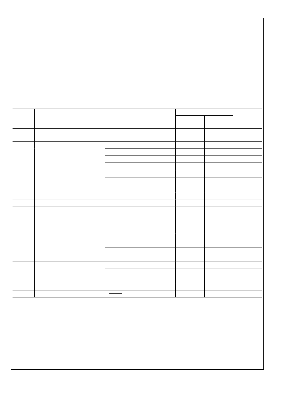
Electrical Characteristics The following specifications apply for A
otherwise specified. Limits apply for TA = 25°C. VDD = 3.6V.
Symbol Parameter Conditions
|VOS|
I
DD
I
SD
V
SDIH
V
SDIL
A
V
R
IN
T
WU
Differential Output Offset Voltage
Quiescent Power Supply Current
Shutdown Current
Shutdown voltage input high For SDR, SDL 1.4 V (min)
Shutdown voltage input low For SDR, SDL 0.4 V (max)
Gain
Input Resistance
Wake Up Time
VI = 0V, AV = 2V/V,
VDD = 2.4V to 5.0V
VIN = 0V, No Load, VDD = 5.0V 5.1 7.5 mA (max)
VIN = 0V, No Load, VDD = 3.6V 4.2 6.0 mA (max)
VIN = 0V, No Load, VDD = 2.4V 3.0 4.5 mA (max)
VIN = 0V, RL = 8Ω, VDD = 5.0V
VIN = 0V, RL = 8Ω, VDD = 3.6V
VIN = 0V, RL = 8Ω, VDD = 2.4V
V
= V
SDL
= GND
SDR
GAIN0, GAIN1 = GND
RL = ∞
GAIN0 = VDD, GAIN1 = GND
RL = ∞
GAIN0 = GND, GAIN1 = V
DD
RL = ∞
GAIN0, GAIN1 = V
DD
RL = ∞
AV = 6dB
AV = 12dB
AV = 18dB
AV = 24dB
V
SDR/SDL
= 0.4V
63.6°C/W
MAX
−40°C ≤ TA ≤ 85°C
2.4V ≤ VDD ≤ 5.5V
= 6dB, RL = 15μH+8Ω, f = 1kHz, unless
V
LM48411
Typical Limit
(Note 6) (Notes 7, 8)
Units
(Limits)
5 mV
5.2 mA
4.2 mA
3.0 mA
0.01 1.0
μA (max)
6 6±0.5 dB
12 12±0.5 dB
18 18±0.5 dB
24 24±0.5 dB
56
37.5
22.5
12.5
4.2
kΩ
kΩ
kΩ
kΩ
ms
5 www.national.com
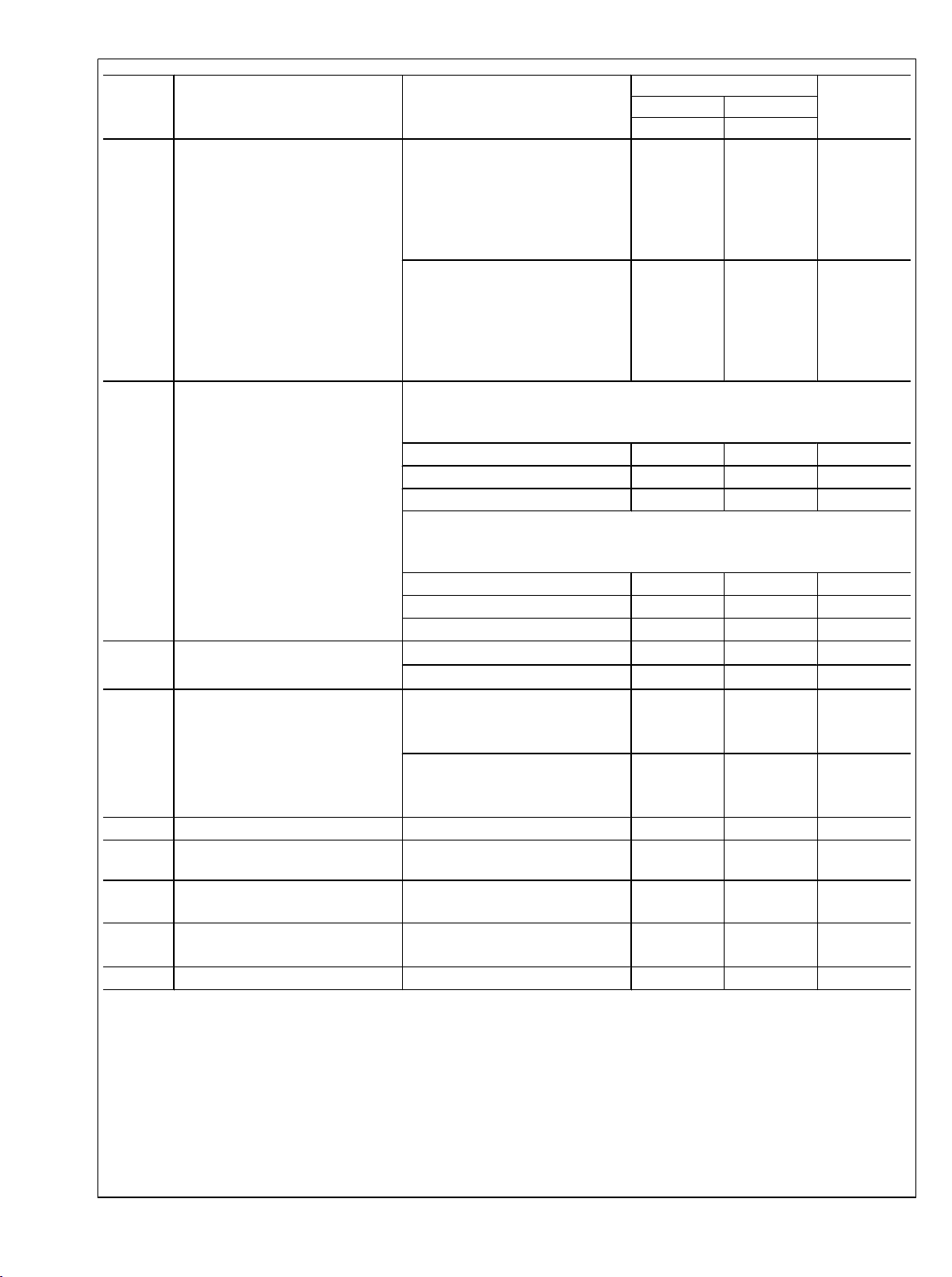
Symbol Parameter Conditions
LM48411
RL = 15μH + 4Ω + 15μH
THD = 10% (max)
f = 1kHz, 22kHz BW
VDD = 5V
VDD = 3.6V
P
O
P
O
Output Power
Output Power
THD+N Total Harmonic Distortion + Noise
PSRR
Power Supply Rejection Ratio
(Input Referred)
SNR Signal to Noise Ratio
ε
OUT
CMRR
η
Output Noise
(Input Referred)
Common Mode Rejection Ratio
(Input Referred)
Efficiency
Xtalk Crosstalk
VDD = 2.5V
RL = 15μH + 4Ω + 15μH
THD = 1% (max)
f = 1kHz, 22kHz BW
VDD = 5V
VDD = 3.6V
VDD = 2.5V
RL = 15μH + 8Ω + 15μH
THD = 10% (max)
f = 1kHz, 22kHz BW
VDD = 5V 1.5 W
VDD = 3.6V 760 600 mW (min)
VDD = 2.5V 330 mW
RL = 15μH + 8Ω + 15μH
THD = 1% (max)
f = 1kHz, 22kHz BW
VDD = 5V 1.25
VDD = 3.6V 615 mW
VDD = 2.5V 270
PO = 500mW, f = 1kHz, RL = 8Ω
PO = 300mW, f = 1kHz, RL = 8Ω
V
= 200mVPP Sine,
Ripple
f
= 217Hz, VDD = 3.6, 5V
Ripple
Inputs to AC GND, CI = 2μF
V
= 200mVPP Sine,
Ripple
f
= 1kHz, VDD = 3.6, 5V
Ripple
Inputs to AC GND, CI = 2μF
VDD = 5V, PO = 1W
VDD = 3.6V, A Weighted
VDD = 3.6V, V
f
= 217Hz
Ripple
VDD = 5V, P
OUT
RL = 8Ω
PO = 500mW, f = kHz
Ripple
= 1W
RMS
= 1V
PP
Sine
LM48411
Typical Limit
(Note 6) (Notes 7, 8)
2.5
1.2
530
2.0
1.0
430
0.05 %
0.03
78
77
96
22
64
88
84
Units
(Limits)
W
W
mW
W
W
mW
W
mW
%
dB
dB
dB
μV
RMS
dB
%
dB
www.national.com 6

Note 1: “Absolute Maximum Ratings” indicate limits beyond which damage to the device may occur, including inoperability and degradation of device reliability
and/or performance. Functional operation of the device and/or non-degradation at the Absolute Absolute Maximum Ratings or other conditions beyond those
indicated in the Recommended Operating Conditions is not implied. The Recommended Operating Conditions indicate conditions at which the device is functional
and the device should not be operated beyond such conditions. All voltages are measured with respect to the ground pin, unless otherwise specified
Note 2: The Electrical Characteristics tables list guaranteed specifications under the listed Recommended Operating Conditions except as otherwise modified
or specified by the Electrical Characteristics Conditions and/or Notes. Typical specifications are estimations only and are not guaranteed.
Note 3: The maximum power dissipation must be derated at elevated temperatures and is dictated by T
allowable power dissipation is P
Derating curves for additional information.
Note 4: Human body model, applicable std. JESD22-A114C.
Note 5: Machine model, applicable std. JESD22-A115-A.
Note 6: Typical values represent most likely parametric norms at TA = +25ºC, and at the Recommended Operation Conditions at the time of product
characterization and are not guaranteed.
Note 7: Datasheet min/max specification limits are guaranteed by test or statistical analysis.
Note 8: Shutdown current is measured in a normal room environment. Exposure to direct sunlight will increase ISD by a maximum of 2µA. The Shutdown pin
should be driven as close as possible to GND for minimal shutdown current and to VDD for the best THD performance in PLAY mode. See the Application
Information section under SHUTDOWN FUNCTION for more information.
Note 9: The performance graphs were taken using the Audio Precision AUX-0025 Switching Amplifier measurement Filter in series with the LC filter on the demo
board.
DMAX
= (T
- TA) / θJA or the number given in Absolute Maximum Ratings, whichever is lower. For the LMxxxxx, see Power
JMAX
, θJA, and the ambient temperature, TA. The maximum
JMAX
Typical Performance Characteristics
LM48411
V
= 2.5V, RL = 8Ω, PO = 100mW/channel
DD
AV = 6dB
THD+N vs Frequency
V
= 5.0V, RL = 8Ω, PO = 375mW/channel
THD+N vs Frequency
DD
AV = 6dB
30009540
V
= 3.6V, RL = 8Ω, PO = 250mW/channel
DD
AV = 6dB
THD+N vs Frequency
V
= 2.5V, RL = 4Ω, PO = 100mW/channel
THD+N vs Frequency
DD
AV = 6dB
30009546
30009549
30009552
7 www.national.com

LM48411
V
THD+N vs Frequency
= 3.6V, RL = 4Ω, PO = 250mW/channel
DD
AV = 6dB
V
THD+N vs Frequency
= 5.0V, RL = 4Ω, PO = 375mW/channel
DD
AV = 6dB
THD+N vs Output Power
V
= 2.5V, RL = 8Ω, AV = 6dB
DD
THD+N vs Output Power
V
= 3.6V, RL = 8Ω, AV = 6dB
DD
30009556
30009574
THD+N vs Output Power
V
= 2.5V, RL = 8Ω, AV = 24dB
DD
THD+N vs Output Power
V
= 3.6V, RL = 8Ω, AV = 24dB
DD
30009558
30009575
30009578
www.national.com 8
30009579

LM48411
THD+N vs Output Power
V
= 5V, RL = 8Ω, AV = 6dB
DD
THD+N vs Output Power
V
= 2.5V, RL = 4Ω, AV = 6dB
DD
30009582
THD+N vs Output Power
V
= 5V, RL = 8Ω, AV = 24dB
DD
THD+N vs Output Power
V
= 2.5V, RL = 4Ω, AV = 24dB
DD
30009583
THD+N vs Output Power
V
= 3.6V, RL = 4Ω, AV = 6dB
DD
30009572
30009576
30009573
THD+N vs Output Power
V
= 3.6V, RL = 4Ω, AV = 24dB
DD
30009577
9 www.national.com

LM48411
THD+N vs Output Power
V
= 5.0V, RL = 4Ω, AV = 6dB
DD
THD+N vs Output Power
V
= 5.0V, RL = 4Ω, AV = 24dB
DD
PSRR vs Frequency
VDD = 3.6V, RL = 8Ω
Quiescent Current vs Power Supply
RL = ∞
30009580
30009568
30009581
CMRR vs Frequency
VDD = 3.6V, RL = 8Ω
30009571
Output Power vs Supply Voltage
RL = 4Ω, f = 1kHz
30009542
www.national.com 10
30009561

LM48411
Output Power vs Supply Voltage
RL = 8Ω, f = 1kHz
Efficiency vs Output Power
RL = 8Ω
30009562
Efficiency vs Output Power
RL = 4Ω
30009569
Crosstalk vs Frequency
VDD = 3.6V, RL = 8Ω
Power Dissipation vs Output Power
RL = 4Ω
30009570
30009566
30009563
Power Dissipation vs Output Power
RL = 8Ω
30009567
11 www.national.com

External Components Description
(Figure 2)
LM48411
Components Functional Description
1. CSSupply bypass capacitor which provides power supply filtering. Refer to the Power Supply Bypassing section
for information concerning proper placement and selection of the supply bypass capacitor.
2. CIInput AC coupling capacitor which blocks the DC voltage at the amplifier's input terminals.
www.national.com 12

Application Information
GENERAL AMPLIFIER FUNCTION
The LM48411 features a filterless modulation scheme. The
differential outputs of the device switch at 300kHz from V
to GND. When there is no input signal applied, the two outputs
(VO1 and VO2) switch with a 50% duty cycle, with both outputs
in phase. Because the outputs of the LM48411 are differential, the two signals cancel each other. This results in no net
voltage across the speaker, thus there is no load current during an idle state, conserving power.
With an input signal applied, the duty cycle (pulse width) of
the LM48411 outputs changes. For increasing output voltages, the duty cycle of VO1 increases, while the duty cycle of
VO2 decreases. For decreasing output voltages, the converse
occurs, the duty cycle of VO2 increases while the duty cycle
of VO1 decreases. The difference between the two pulse
widths yields the differential output voltage.
SPREAD SPECTRUM MODULATION
The LM48411 features a fitlerless spread spectrum modulation scheme that eliminates the need for output filters, ferrite
beads or chokes. The switching frequency varies by ±30%
about a 300kHz center frequency, reducing the wideband
spectral contend, improving EMI emissions radiated by the
speaker and associated cables and traces. Where a fixed frequency class D exhibits large amounts of spectral energy at
multiples of the switching frequency, the spread spectrum architecture of the LM48411 spreads that energy over a larger
bandwidth. The cycle-to-cycle variation of the switching period does not affect the audio reproduction of efficiency.
ENHANCED EMISSIONS SUPPRESSION SYSTEM (E2S)
The LM48411 features National’s patent-pending E2S system
that reduces EMI, while maintaining high quality audio reproduction and efficiency. The E2S system features a synchronizable oscillator with selectable spread spectrum, and
advanced edge rate control (ERC). The LM48411 ERC greatly reduces the high frequency components of the output
square waves by controlling the output rise and fall times,
slowing the transitions to reduce RF emissions, while maximizing THD+N and efficiency performance.
POWER DISSIPATION AND EFFICIENCY
In general terms, efficiency is considered to be the ratio of
useful work output divided by the total energy required to produce it with the difference being the power dissipated, typically, in the IC. The key here is “useful” work. For audio
systems, the energy delivered in the audible bands is considered useful including the distortion products of the input
signal. Sub-sonic (DC) and super-sonic components
(>22kHz) are not useful. The difference between the power
flowing from the power supply and the audio band power being transduced is dissipated in the LM48411 and in the transducer load. The amount of power dissipation in the LM48411
is very low. This is because the ON resistance of the switches
used to form the output waveforms is typically less than
0.25Ω. This leaves only the transducer load as a potential
"sink" for the small excess of input power over audio band
output power. The LM48411 dissipates only a fraction of the
excess power requiring no additional PCB area or copper
plane to act as a heat sink.
DD
LM48411
DIFFERENTIAL AMPLIFIER EXPLANATION
As logic supply voltages continue to shrink, designers are increasingly turning to differential analog signal handling to
preserve signal to noise ratios with restricted voltage swing.
The LM48411 is a fully differential amplifier that features differential input and output stages. A differential amplifier amplifies the difference between the two input signals. Traditional audio power amplifiers have typically offered only singleended inputs resulting in a 6dB reduction in signal to noise
ratio relative to differential inputs. The LM48411 also offers
the possibility of DC input coupling which eliminates the two
external AC coupling, DC blocking capacitors. The LM48411
can be used, however, as a single ended input amplifier while
still retaining it's fully differential benefits. In fact, completely
unrelated signals may be placed on the input pins. The
LM48411 simply amplifies the difference between the signals.
A major benefit of a differential amplifier is the improved common mode rejection ratio (CMRR) over single input amplifiers.
The common-mode rejection characteristic of the differential
amplifier reduces sensitivity to ground offset related noise injection, especially important in high noise applications.
PCB LAYOUT CONSIDERATIONS
As output power increases, interconnect resistance (PCB
traces and wires) between the amplifier, load and power supply create a voltage drop. The voltage loss on the traces
between the LM48411 and the load results is lower output
power and decreased efficiency. Higher trace resistance between the supply and the LM48411 has the same effect as a
poorly regulated supply, increased ripple on the supply line
also reducing the peak output power. The effects of residual
trace resistance increases as output current increases due to
higher output power, decreased load impedance or both. To
maintain the highest output voltage swing and corresponding
peak output power, the PCB traces that connect the output
pins to the load and the supply pins to the power supply
should be as wide as possible to minimize trace resistance.
The use of power and ground planes will give the best THD
+N performance. While reducing trace resistance, the use of
power planes also creates parasite capacitors that help to filter the power supply line.
The inductive nature of the transducer load can also result in
overshoot on one or both edges, clamped by the parasitic
diodes to GND and VDD in each case. From an EMI standpoint, this is an aggressive waveform that can radiate or
conduct to other components in the system and cause interference. It is essential to keep the power and output traces
short and well shielded if possible. Use of ground planes,
beads, and micro-strip layout techniques are all useful in preventing unwanted interference.
As the distance from the LM48411 and the speaker increase,
the amount of EMI radiation will increase since the output
wires or traces acting as antenna become more efficient with
length. What is acceptable EMI is highly application specific.
Ferrite chip inductors placed close to the LM48411 may be
needed to reduce EMI radiation. The value of the ferrite chip
is very application specific.
13 www.national.com

SHUTDOWN FUNCTION
In order to reduce power consumption while not in use, the
LM48411 contains shutdown circuitry that reduces current
LM48411
draw to less than 0.01µA. The trigger point for shutdown is
shown as a typical value in the Electrical Characteristics Tables and in the Shutdown Hysteresis Voltage graphs found in
the Typical Performance Characteristics section. It is best
to switch between ground and supply for minimum current
usage while in the shutdown state. While the LM48411 may
be disabled with shutdown voltages in between ground and
supply, the idle current will be greater than the typical 0.01µA
value.
The LM48411 has an internal resistor connected between
GND and Shutdown pins. The purpose of this resistor is to
eliminate any unwanted state changes when the Shutdown
pin is floating. The LM48411 will enter the shutdown state
when the Shutdown pin is left floating or if not floating, when
the shutdown voltage has crossed the threshold. To minimize
the supply current while in the shutdown state, the Shutdown
pin should be driven to GND or left floating. If the Shutdown
pin is not driven to GND, the amount of additional resistor
current due to the internal shutdown resistor can be found by
Equation (1) below.
(VSD - GND) / 300kΩ (1)
With only a 0.5V difference, an additional 1.7µA of current will
be drawn while in the shutdown state.
AUDIO AMPLIFIER POWER SUPPLY BYPASSING FILTERING
Proper power supply bypassing is critical for low noise performance and high PSRR. Place the supply bypass capacitor
as close to the device as possible. Typical applications employ a voltage regulator with 10µF and 0.1µF bypass capacitors that increase supply stability. These capacitors do not
eliminate the need for bypassing of the LM48411 supply pins.
A 1µF capacitor is recommended.
AUDIO AMPLIFIER INPUT CAPACITOR SELECTION
Input capacitors may be required for some applications, or
when the audio source is single-ended. Input capacitors block
the DC component of the audio signal, eliminating any conflict
between the DC component of the audio source and the bias
voltage of the LM48411. The input capacitors create a highpass filter with the input resistance Ri. The -3dB point of the
high pass filter is found using Equation 1 below.
f = 1 / 2πRiC
The values for Ri can be found in the EC table for each gain
setting.
The input capacitors can also be used to remove low frequency content from the audio signal. Small speakers cannot
reproduce, and may even be damaged by low frequencies.
High pass filtering the audio signal helps protect the speakers.
When the LM48411 is using a single-ended source, power
supply noise on the ground is seen as an input signal. Setting
the high-pass filter point above the power supply noise frequencies, 217 Hz in a GSM phone, for example, filters out the
noise such that it is not amplified and heard on the output.
Capacitors with a tolerance of 10% or better are recommended for impedance matching and improved CMRR and PSRR.
AUDIO AMPLIFIER GAIN SETTING
The LM48411 features four internally configured gain settings. The device gain is selected through the two logic inputs,
G0 and G1. The gain settings are as shown in the following
table.
LOGIC INPUT GAIN
G1 G0 V/V dB
0 0 2 6
0 1 4 12
1 0 8 18
1 1 16 24
i
(2)
Build of Materials
Designator Description Footprint Quantity
C1, C2
C3 – C6
C11
JP1–5, JP8–11 Jumper Header Vertical Mount 2X1 0.100 9
JP6, JP7 Jumper Header Vertical Mount 3x1 0.100 2
www.national.com 14
Ceramic Capacitor 0.1μF, 50V, 10%
Tantalum Capacitors 1μF 20V, 10%, Size A
Tantalum Capacitors 10μF 20V, 10% Size B
805 2
1206 4
1411 1

Demonstration Board Schematic
LM48411
30009592
15 www.national.com

Demonstration Board Layout
LM48411
Top Silkscreen Layer
Top Layer
30009591
30009590
Mid 1 Layer
www.national.com 16
30009588

LM48411
Mid 2 Layer
Bottom Layer
30009589
30009587
17 www.national.com

Revision History
LM48411
Rev Date Description
1.0 09/21/07 Initial release.
1.1 10/01/07 Fixed few typos.
1.2 11/30/07 Added the demo boards and BOM.
1.3 12/19/07 Edited the 16–bump micro SMD package diagram and the Pin Description table.
1.4 01/08/08 Edited the 16–bump micro SMD package diagram.
1.5 06/27/08 Text edits.
1.6 07/03/08 Text edits (under SHUTDOWN FUNCTION).
www.national.com 18

Physical Dimensions inches (millimeters) unless otherwise noted
LM48411
16 Bump micro SMD
Order Number LM48411TL
NS Package Number TLA16ACA
X1 = 1.996mm X2 = 2.047mm X3 = 0.6mm
19 www.national.com

S
2
Notes
For more National Semiconductor product information and proven design tools, visit the following Web sites at:
Products Design Support
Amplifiers www.national.com/amplifiers WEBENCH www.national.com/webench
Audio www.national.com/audio Analog University www.national.com/AU
Clock Conditioners www.national.com/timing App Notes www.national.com/appnotes
Data Converters www.national.com/adc Distributors www.national.com/contacts
Displays www.national.com/displays Green Compliance www.national.com/quality/green
Ethernet www.national.com/ethernet Packaging www.national.com/packaging
Interface www.national.com/interface Quality and Reliability www.national.com/quality
LVDS www.national.com/lvds Reference Designs www.national.com/refdesigns
Power Management www.national.com/power Feedback www.national.com/feedback
Switching Regulators www.national.com/switchers
LDOs www.national.com/ldo
LED Lighting www.national.com/led
PowerWise www.national.com/powerwise
Serial Digital Interface (SDI) www.national.com/sdi
Temperature Sensors www.national.com/tempsensors
Wireless (PLL/VCO) www.national.com/wireless
THE CONTENTS OF THIS DOCUMENT ARE PROVIDED IN CONNECTION WITH NATIONAL SEMICONDUCTOR CORPORATION
(“NATIONAL”) PRODUCTS. NATIONAL MAKES NO REPRESENTATIONS OR WARRANTIES WITH RESPECT TO THE ACCURACY
OR COMPLETENESS OF THE CONTENTS OF THIS PUBLICATION AND RESERVES THE RIGHT TO MAKE CHANGES TO
SPECIFICATIONS AND PRODUCT DESCRIPTIONS AT ANY TIME WITHOUT NOTICE. NO LICENSE, WHETHER EXPRESS,
IMPLIED, ARISING BY ESTOPPEL OR OTHERWISE, TO ANY INTELLECTUAL PROPERTY RIGHTS IS GRANTED BY THIS
DOCUMENT.
TESTING AND OTHER QUALITY CONTROLS ARE USED TO THE EXTENT NATIONAL DEEMS NECESSARY TO SUPPORT
NATIONAL’S PRODUCT WARRANTY. EXCEPT WHERE MANDATED BY GOVERNMENT REQUIREMENTS, TESTING OF ALL
PARAMETERS OF EACH PRODUCT IS NOT NECESSARILY PERFORMED. NATIONAL ASSUMES NO LIABILITY FOR
APPLICATIONS ASSISTANCE OR BUYER PRODUCT DESIGN. BUYERS ARE RESPONSIBLE FOR THEIR PRODUCTS AND
APPLICATIONS USING NATIONAL COMPONENTS. PRIOR TO USING OR DISTRIBUTING ANY PRODUCTS THAT INCLUDE
NATIONAL COMPONENTS, BUYERS SHOULD PROVIDE ADEQUATE DESIGN, TESTING AND OPERATING SAFEGUARDS.
EXCEPT AS PROVIDED IN NATIONAL’S TERMS AND CONDITIONS OF SALE FOR SUCH PRODUCTS, NATIONAL ASSUMES NO
LIABILITY WHATSOEVER, AND NATIONAL DISCLAIMS ANY EXPRESS OR IMPLIED WARRANTY RELATING TO THE SALE
AND/OR USE OF NATIONAL PRODUCTS INCLUDING LIABILITY OR WARRANTIES RELATING TO FITNESS FOR A PARTICULAR
PURPOSE, MERCHANTABILITY, OR INFRINGEMENT OF ANY PATENT, COPYRIGHT OR OTHER INTELLECTUAL PROPERTY
RIGHT.
LIFE SUPPORT POLICY
NATIONAL’S PRODUCTS ARE NOT AUTHORIZED FOR USE AS CRITICAL COMPONENTS IN LIFE SUPPORT DEVICES OR
SYSTEMS WITHOUT THE EXPRESS PRIOR WRITTEN APPROVAL OF THE CHIEF EXECUTIVE OFFICER AND GENERAL
COUNSEL OF NATIONAL SEMICONDUCTOR CORPORATION. As used herein:
Life support devices or systems are devices which (a) are intended for surgical implant into the body, or (b) support or sustain life and
whose failure to perform when properly used in accordance with instructions for use provided in the labeling can be reasonably expected
to result in a significant injury to the user. A critical component is any component in a life support device or system whose failure to perform
can be reasonably expected to cause the failure of the life support device or system or to affect its safety or effectiveness.
National Semiconductor and the National Semiconductor logo are registered trademarks of National Semiconductor Corporation. All other
brand or product names may be trademarks or registered trademarks of their respective holders.
Copyright© 2008 National Semiconductor Corporation
For the most current product information visit us at www.national.com
LM48411 Ultra-Low EMI, Filterless, 2.5W, Stereo, Class D Audio Power Amplifier with E
www.national.com
National Semiconductor
Americas Technical
Support Center
Email: support@nsc.com
Tel: 1-800-272-9959
National Semiconductor Europe
Technical Support Center
Email: europe.support@nsc.com
German Tel: +49 (0) 180 5010 771
English Tel: +44 (0) 870 850 4288
National Semiconductor Asia
Pacific Technical Support Center
Email: ap.support@nsc.com
National Semiconductor Japan
Technical Support Center
Email: jpn.feedback@nsc.com
 Loading...