February 2007
LM48410
Low-EMI, Filterless, 2.3W Stereo Class D Audio Power
Amplifier with National 3D Enhancement
LM48410 Low-EMI, Filterless, 2.3W Stereo Class D Audio Power Amplifier with National 3D
Enhancement
General Description
The LM48410 is a single supply, high efficiency, 2.3W/channel, filterless switching audio amplifier. A low noise PWM
architecture eliminates the output filter, reducing external
component count, board area consumption, system cost, and
simplifying design. A selectable spread spectrum modulation
scheme suppresses RF emissions, further reducing the need
for output filters.
The LM48410 is designed to meet the demands of mobile
phones and other portable communication devices. Operating from a single 5V supply, the device is capable of delivering
2.3W/channel of continuous output power to a 4Ω load with
less than 10% THD+N. Flexible power supply requirements
allow operation from 2.4V to 5.5V. The LM48410 offers two
logic selectable modulation schemes, fixed frequency mode,
and an EMI suppressing spread spectrum mode.
The LM48410 features high efficiency compared with conventional Class AB amplifiers. When driving an 8Ω speaker
from a 3.6V supply, the device operates with 85% efficiency
at PO = 500mW. Four gain options are pin selectable through
the GAIN0 and GAIN1 pins. The LM48410 also includes
National’s 3D audio enhancement that improves stereo
sound quality. In devices where the left and right speakers are
in close proximity, 3D enhancement affects channel specialization, widening the perceived soundstage.
Output short circuit protection prevents the device from being
damaged during fault conditions. Superior click and pop suppression eliminates audible transients on power-up/down and
during shutdown. Independent left/right shutdown controls
maximizes power savings in mixed mono/stereo applications.
Key Specifications
■ Quiescent Power Supply Current
at 3.6V supply 4mA
■ Power Output at V
RL = 4Ω, THD ≤ 10%
■ Power Output at V
RL = 8Ω, THD ≤ 10%
■ Shutdown current
■ Efficiency at 3.6V, 100mW into 8Ω
■ Efficiency at 3.6V, 100mW into 8Ω
■ Efficiency at 5V, 1W into 8Ω
DD
DD
= 5V,
= 5V,
2.3W (typ)
1.5W (typ)
0.03μA (typ)
80% (typ)
85% (typ)
86% (typ)
Features
Selectable spread spectrum mode reduces EMI
■
Output Short Circuit Protection
■
Stereo Class D operation
■
No output filter required
■
National 3D Enhancement
■
Logic selectable gain
■
Independent shutdown control
■
Minimum external components
■
Click and Pop suppression
■
Micro-power shutdown
■
Available in space-saving 4mm x 4mm LLP package
■
Applications
Mobile phones
■
PDAs
■
Laptops
■
EMI Plot
300106a0
Boomer® is a registered trademark of National Semiconductor Corporation.
© 2007 National Semiconductor Corporation 300106 www.national.com

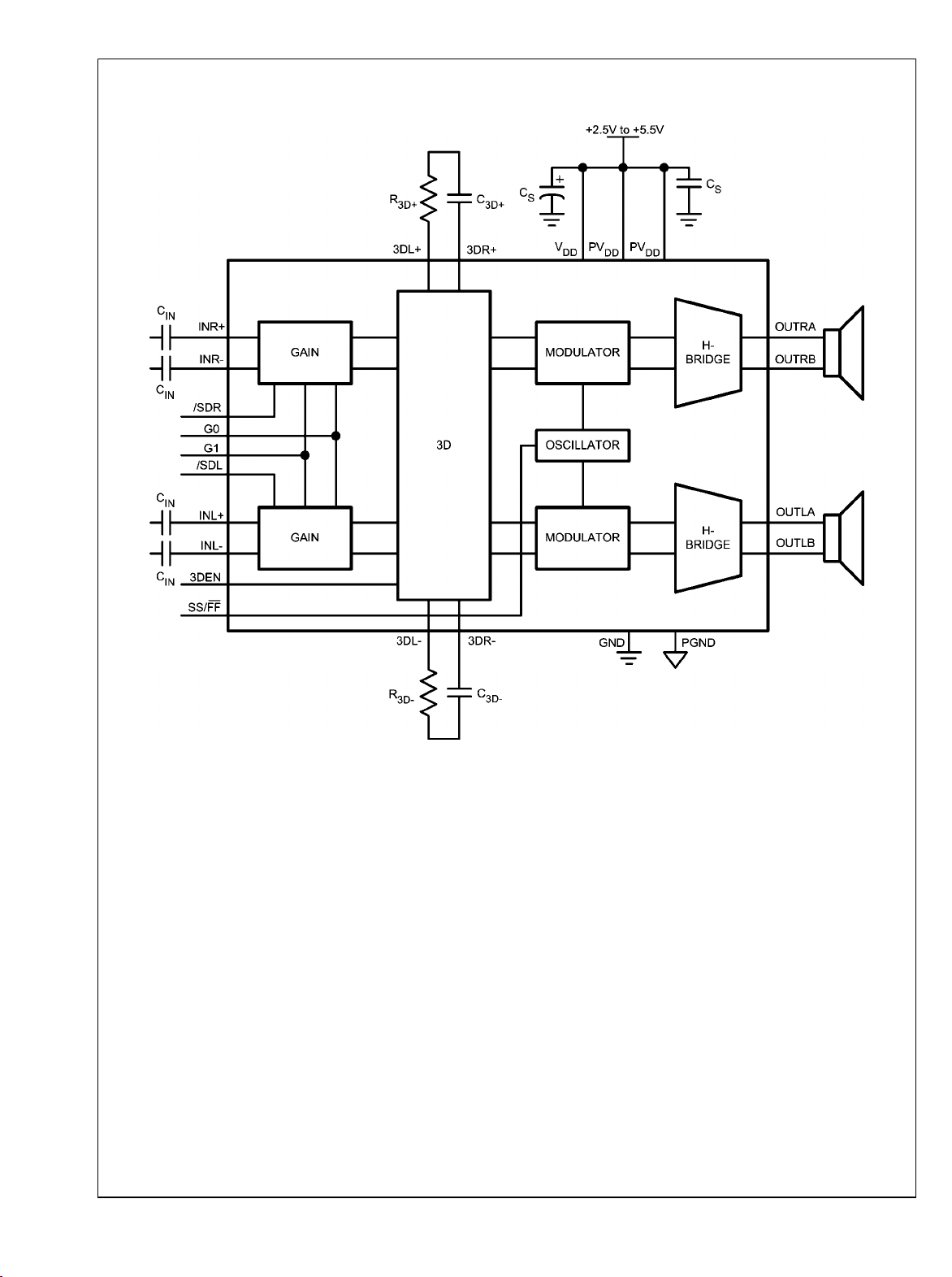
Typical Application
LM48410
FIGURE 1. Typical Audio Amplifier Application Circuit
www.national.com 2
30010686

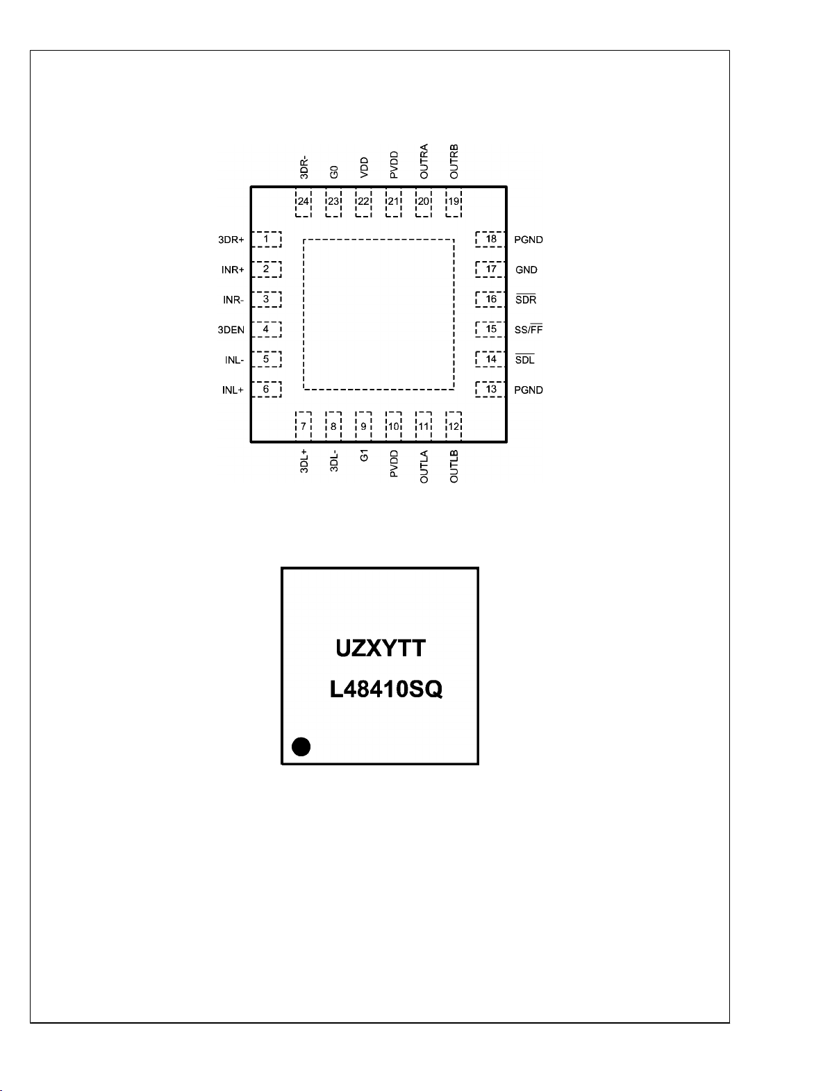
Connection Diagrams
LM48410
LLP Package
4mm x 4mm x 0.8mm
Order Number LM48410SQ
Top View
See NS Package Number SQA24A
LM48410SQ Markings
Top View
30010699
U = Wafer Fab Code
Z = Assembly Plant
XY = 2 Digit Date Code
TT = Lot Traceability
L48410SQ = LM48410SQ
30010685
3 www.national.com

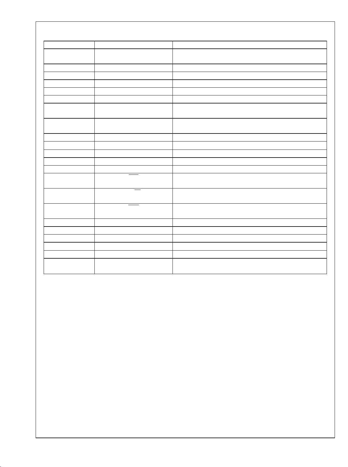
Pin Descriptions
LM48410
Pin Name Description
1 3DR+ Right Channel non-inverting 3D connection. Connect to 3DL+ through
C
and R
3D+
3D+
2 INR+ Right Channel Non-Inverting Input
3 INR- Right Channel Inverting Input
4 3DEN 3D Enable Input
5 INL- Left Channel Inverting Input
6 INL+ Left Channel Non-Inverting Input
7 3DL+ Left Channel non-inverting 3D connection. Connect to 3DR+ through
C
and R
3D+
3D+
8 3DL- Left Channel non-inverting 3D connection. Connect to 3DR- through
C
and R
3D-
3D-
9 G1 Gain Select Input 1
10, 21 PV
DD
Speaker Power Supply
11 OUTLA Left Channel Non-Inverting Output
12 OUTLB Left Channel Inverting Output
13, 18 PGND Power Ground
14 SDL Left Channel Active Low Shutdown. Connect to VDD for normal
operation. Connect to GND to disable the left channel.
15 SS/FF Modulation Mode Select. Connect to VDD for spread spectrum mode.
Connect to GND for fixed frequency mode
16 SDR Right Channel Active Low Shutdown. Connect to VDD for normal
operation. Connect to GND to disable the right channel.
17 GND Ground
19 OUTRB Right Channel Inverting Output
20 OUTRA Right Channel Non-Inverting Output
22 V
DD
Power Supply
23 G0 Gain Select Input 0
24 3DR- Right Channel muting 3D connection. Connect to 3DL- through C
and R
3D-
3D-
www.national.com 4

LM48410
Absolute Maximum Ratings (Notes 1, 2)
If Military/Aerospace specified devices are required,
please contact the National Semiconductor Sales Office/
Distributors for availability and specifications.
Junction Temperature 150°C
Thermal Resistance
θJC (TBD)
θJA (TBD)
5.3°C/W
36.5°C/W
Supply Voltage (Note 1) 6.0V
Storage Temperature −65°C to +150°C
Input Voltage –0.3V to VDD +0.3V
Power Dissipation (Note 3) Internally Limited
ESD Susceptibility(Note 4) 2000V
ESD Susceptibility (Note 5) 200V
Operating Ratings (Notes 1, 2)
Temperature Range
T
≤ TA ≤ T
MIN
MAX
Supply Voltage (VDD, PVDD)
−40°C ≤ TA ≤ 85°C
2.4V ≤ VDD ≤ 5.5V
Electrical Characteristics VDD = PVDD = 3.6V (Notes 1, 2) The following specifications apply for
AV = 6dB, RL = 15μH + 8Ω + 15μH, SS/FF = VDD = (Spread Spectrum mode), f = 1kHz, unless otherwise specified. Limits apply
for TA = 25°C.
LM48410
Symbol Parameter Conditions
V
OS
Differential Output Offset Voltage
VIN = 0, VDD = 2.4V to 5.0V
VIN = 0, RL = ∞,
I
DD
Quiescent Power Supply Current
Both channels active, VDD = 3.6V
VIN = 0, RL = ∞,
Both channels active, VDD = 5V
I
SD
V
IH
V
IL
T
WU
f
SW
Shutdown Current
Logic Input High Voltage 1.4 V (min)
Logic Input Low Voltage 0.4 V (max)
Wake Up Time 4 ms
Switching Frequency
V
= GND
SD_
SS/FF = V
(Spread Spectrum) 300+30% kHz
DD
SS/FF = GND (Fixed Frequency) 300 kHz
GAIN0, GAIN1 = GND
RL = ∞
GAIN0 = VDD, GAIN1 = GND
A
V
Gain
RL = ∞
GAIN0 = GND, GAIN1 = V
RL = ∞
GAIN0, GAIN1 = V
DD
RL = ∞
AV = 6dB
R
IN
Input Resistance
AV = 12dB
AV = 18dB
AV = 24dB
DD
Typical Limit
(Note 6) (Notes 7, 8)
5 mV
4 6.5 mA
5 8.5 mA
0.03 1
6 6 ± 0.5 dB
12 12 ± 0.5 dB
18 18 ± 0.5 dB
24 24 ± 0.5 dB
160
80
40
20
(Limits)
Units
μA
kΩ
kΩ
kΩ
kΩ
5 www.national.com
 Loading...