

National Semiconductor LM4681 User Manual
LM4681 Demonstration
Board User’s Guide
LM4681 Demonstration Board User’s Guide AN-1488
National Semiconductor
Application Note 1488
Kevin Hoskins
May 2006
Quick Start Guide
Connect the I2C signal generation and interface board to a
computer’s parallel port.
Install LM4681 control software: “LM4681_Software_ver1-
1.”
Apply a 3.0V to 5.0V power supply’s positive voltage output
to the “I2CVDD” pin on jumper JP6. Apply the power supply’s
ground return to the “GND“ pin on JP6.
Apply a 9.0V to 15.5V power supply’s positive voltage output
to the “VDD” pin on JP1. Apply the power supply’s ground
return to the “GND” pin on JP1.
Connect the supplied 5-wire cable between the I
generation and interface board and the 5-pin connector
(JP7) on the LM4681 demonstration board.
Apply a stereo audio signal to jumpers JP4 and JP2. Apply
the source’s signal and ground to the “IN1” pin and the
“GND“ pin, respectively.
2
C signal
Connect a load (≥ 8Ω) between the pins on JP5 and another
load between the pins on JP3.
Apply power. Make measurements. Plug in a pair of headphones. Enjoy.
Introduction
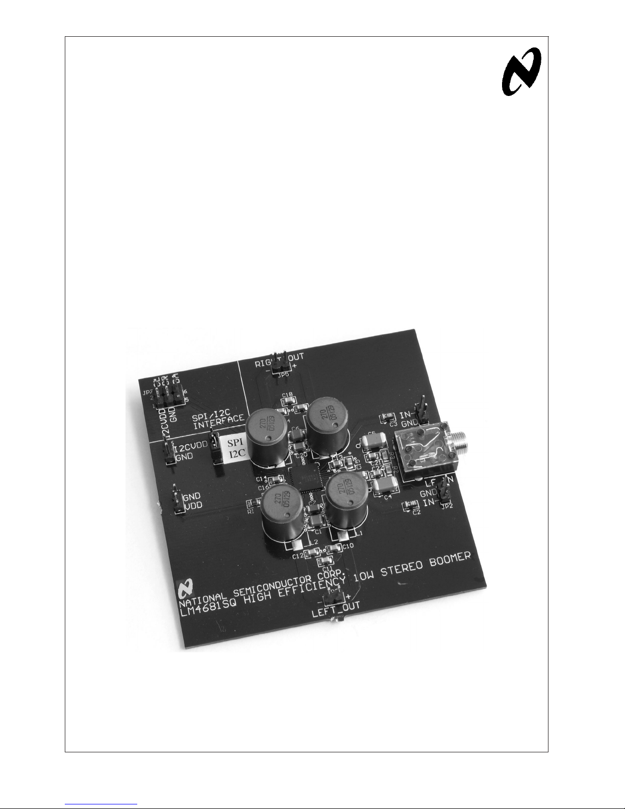
To help the user investigate and evaluate the LM4681’s
performance and capabilities, a fully populated demonstration board is available from the Audio Products Group. This
board is shown in Figure 1. Connected to an external power
supply, a signal source and an I
source), the LM4681 demonstration board easily demonstrates the amplifier’s features.
2
C or SPI controller (or signal
© 2006 National Semiconductor Corporation AN201959 www.national.com
20195901
FIGURE 1. The LM4681 Demonstration Board

General Description
The LM4681 is a Class D audio amplifier with an internal,
AN-1488
digitally controlled volume control, and Class AB stereo
headphone amplifier. The LM4681 is optimized to operate
over a power supply voltage range of 9.0V to 15.5V. This
amplifier is capable of delivering 10W
an 8Ω load at 10% THD when powered by a 14.0V power
supply.
Boomer audio power amplifiers were designed specifically to
provide high quality output power with a minimal amount of
external components. The LM4681 is a high-efficiency Class
D amplifier that is optimally suited for volume minimized
design such as flat panel displays that can not tolerate
heatsinks or portable system that must maximize battery life
while producing high acoustic output.
The LM4681 includes a digitally controlled (I
volume control that optimizes system cost and minimizes
PCB area.
The LM4681 features a shutdown mode for micropower
dissipation, an internal thermal shutdown protection mechanism, and output stage fault detect and current limit protection.
per channel into
RMS
Operating Conditions
Temperature Range –40˚C ≤ TA≤ 85˚C
•
Amplifier Power Supply Voltage 9.0V ≤ VDD≤ 15.5V
•
2
C) 32–step
Board Features
The LM4681 demonstration board has all of the necessary
connections, using 100mil headers, to apply the power supply voltage, the audio input signals, and the I
The Class D amplifier’s output is available on 100 mil headers. The Class AB headphone’s amplified audio signal is
available on both a stereo headphone jack and 100 mil
headers.
Also included with the demonstration board is an I
generation board and software. With this board and the
software, the user can easily control the LM4681’s shutdown
function and stereo volume control. Figure 3 shows the
software’s graphical user interface.
2
C signal inputs.
2
C signal
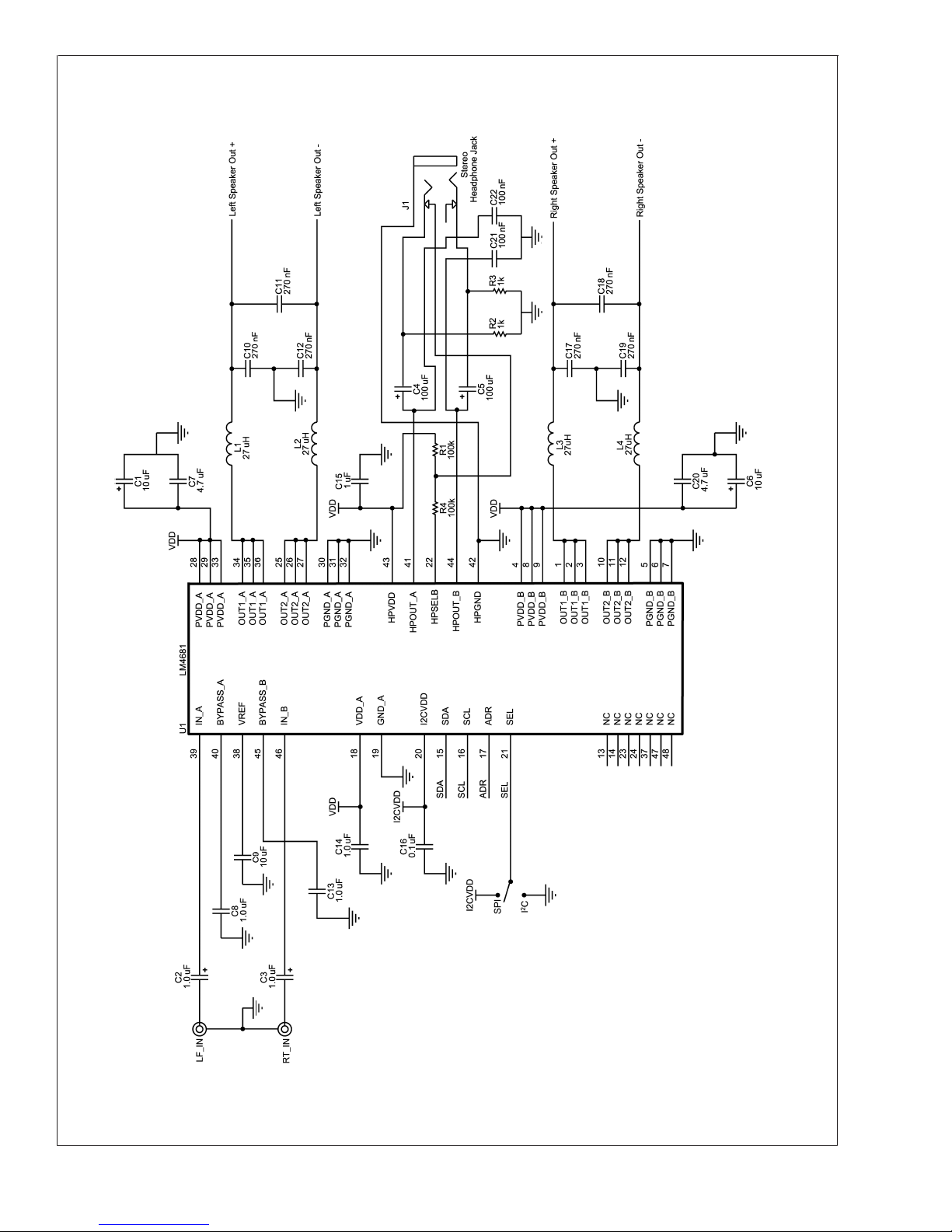
Schematic
Figure 2 shows the LM4681 Demonstration Board schematic. Refer to Table 1 for a list of the connections and their
functions.
www.national.com 2
20195908
AN-1488
Schematic (Continued)
Figure 2. The LM4681 Demonstration Board Schematic
www.national.com3
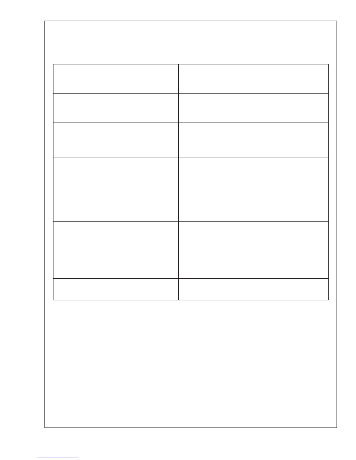
Connections
Connecting to the world is accomplished through the 100mil headers on the LM4681 demonstration board. The functions of the
AN-1488
different headers are detailed in Table 1.
TABLE 1. LM4681 Demonstration Board Connections
Jumper Designation Function or Use
JP1 Power supply connection. Connect an external power supply’s
positive voltage source to the JP1 pin labeled “VDD” and the
supply’s ground source to the pin labeled “GND.”
JP2 This is the connection to the amplifier’s input A (labeled as the
“LF_IN” input on the demonstration board). Apply an external
signal source’s positive voltage to the JP2 pin labeled “IN” and the
signal source’s ground reference to the pin labeled “GND.”
JP3 This is the connection to the amplifier’s output A (labeled as the
"LEFT_OUT” output on the demonstration board). Connect the JP3
pin labeled “+” to the positive input of an external signal
measurement device. Connect the JP3 pin labeled “-” to the
negative input of an external signal measurement device.
JP4 This is the connection to the amplifier’s input B (labeled as the
“RT_IN” input on the demonstration board). Apply an external
signal source’s positive voltage to the JP4 pin labeled “IN” and the
signal source’s ground reference to the pin labeled “GND.”
JP5 This is the connection to the amplifier’s output B (labeled as the
“RIGHT_OUT” output on the demonstration board). Connect the
JP5 pin labeled “+” to the positive input of an external signal
measurement device. Connect the JP5 pin labeled “-” to the
JP6 If an external I
JP7 This header is used for the I
JP8 This three-pin jumper selects either I
Power Supply Sequencing
The LM4681 uses two power supply voltage: VDDfor the
Class D power amplifier and the Class AB headphone amplifier and I
etc.). To ensure proper functionality, apply I
lowed by V
2
CVDDfor the digital controls (volume, shutdown,
. The part will power-up with shutdown active,
DD
2
CVDDfirst, fol-
the volume control set to minimum, and mute active.
I2C Signal Generation Board and
Software
The I2C signal generation and interface board, along with the
LM4681 software, will generate the address byte and the
negative input of an external signal measurement device.
supply’s positive voltage source to the JP6 pin labeled “I2CVDD”
and the supply’s ground source to the pin labeled “GND.” If no
external supply is used, leave this jumper’s pins unconnected.
2
CVDDthat is generated by the I2C signal source, JP7-pin 2 is for
I
the SCL signal, JP7-pin 3 is for GND, JP7-pin 4 is for the ADR
signal, and JP7-pin 6 is for the SDA signal.
protocol. Short pins 1 and 2 together SPI protocol is used. Short
pins 2 and 3 together when I
2
C power supply voltage is used, connect this
2
C signal inputs. JP7-pin 1 is for an
2
C or SPI digital interface
2
C protocol is used.
data byte used in the I
2
C signal generation and interface board, please plug it into
I
2
C control data transaction. To use the
a PC’s parallel port (on either a notebook or a desktop
computer).
The software comes with an installer. To install, unzip the file
titled “LM4681_Software_ver1-1.” After the file unzips,
double-click the “setup.exe” file. After it launches, please
follow the installer’s instructions. Setup will create a folder
named “LM4681” in the “Program” folder on the “C” disk (if
the default is used) along with a shortcut of the same name
in the “Programs” folder in the “Start” menu.
www.national.com 4
 Loading...