

July 2, 2008
LM4674
Filterless 2.5W Stereo Class D Audio Power Amplifier
LM4674 Filterless 2.5W Stereo Class D Audio Power Amplifier
General Description
The LM4674 is a single supply, high efficiency, 2.5W/channel,
filterless switching audio amplifier. A low noise PWM architecture eliminates the output filter, reducing external component count, board area consumption, system cost, and
simplifying design.
The LM4674 is designed to meet the demands of mobile
phones and other portable communication devices. Operating from a single 5V supply, the device is capable of delivering
2.5W/channel of continuous output power to a 4Ω load with
less than 10% THD+N. Flexible power supply requirements
allow operation from 2.4V to 5.5V.
The LM4674 features high efficiency compared to conventional Class AB amplifiers. When driving an 8Ω speaker from
a 3.6V supply, the device features 85% efficiency at PO =
500mW. Four gain options are pin selectable through the G0
and G1 pins.
Output short circuit protection prevents the device from being
damaged during fault conditions. Superior click and pop suppression eliminates audible transients on power-up/down and
during shutdown. Independent left/right shutdown control
maximizes power savings in mixed mono/stereo applications.
Key Specifications
■ Efficiency at 3.6V, 100mW into 8Ω 80% (typ)
■ Efficiency at 3.6V, 500mW into 8Ω 85% (typ)
■ Efficiency at 5V, 1W into 8Ω 85% (typ)
■ Quiescent Power Supply Current
at 3.6V supply 4mA
■ Power Output at V
RL = 4Ω, THD ≤ 10%
■ Power Output at V
RL = 8Ω, THD ≤ 10%
■ Shutdown current
DD
DD
= 5V,
= 5V,
2.5W (typ)
1.5W (typ)
0.03μA (typ)
Features
Output Short Circuit Protection
■
Stereo Class D operation
■
No output filter required
■
Logic selectable gain
■
Independent shutdown control
■
Minimum external components
■
Click and Pop suppression
■
Micro-power shutdown
■
Available in space-saving 2mm x 2mm x 0.6mm micro
■
SMD, and 4mm x 4mm x 0.8mm LLP packages
Applications
Mobile phones
■
PDAs
■
Laptops
■
Boomer® is a registered trademark of National Semiconductor Corporation.
© 2008 National Semiconductor Corporation 201674 www.national.com
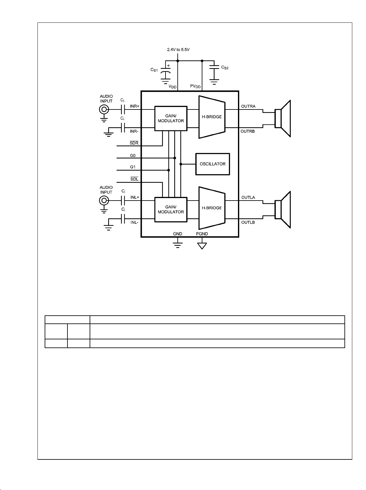
Typical Application
LM4674
20167463
Ci = 1 μF
CS1 = 1 μF
CS2 = 0.1 μF
FIGURE 1. Typical Audio Amplifier Application Circuit
External Components Description
(Figure 1)
Components Functional Description
1. CSSupply bypass capacitor which provides power supply filtering. Refer to the Power Supply Bypassing section
for information concerning proper placement and selection of the supply bypass capacitor.
2. CiInput AC coupling capacitor which blocks the DC voltage at the amplifier's input terminals.
www.national.com 2
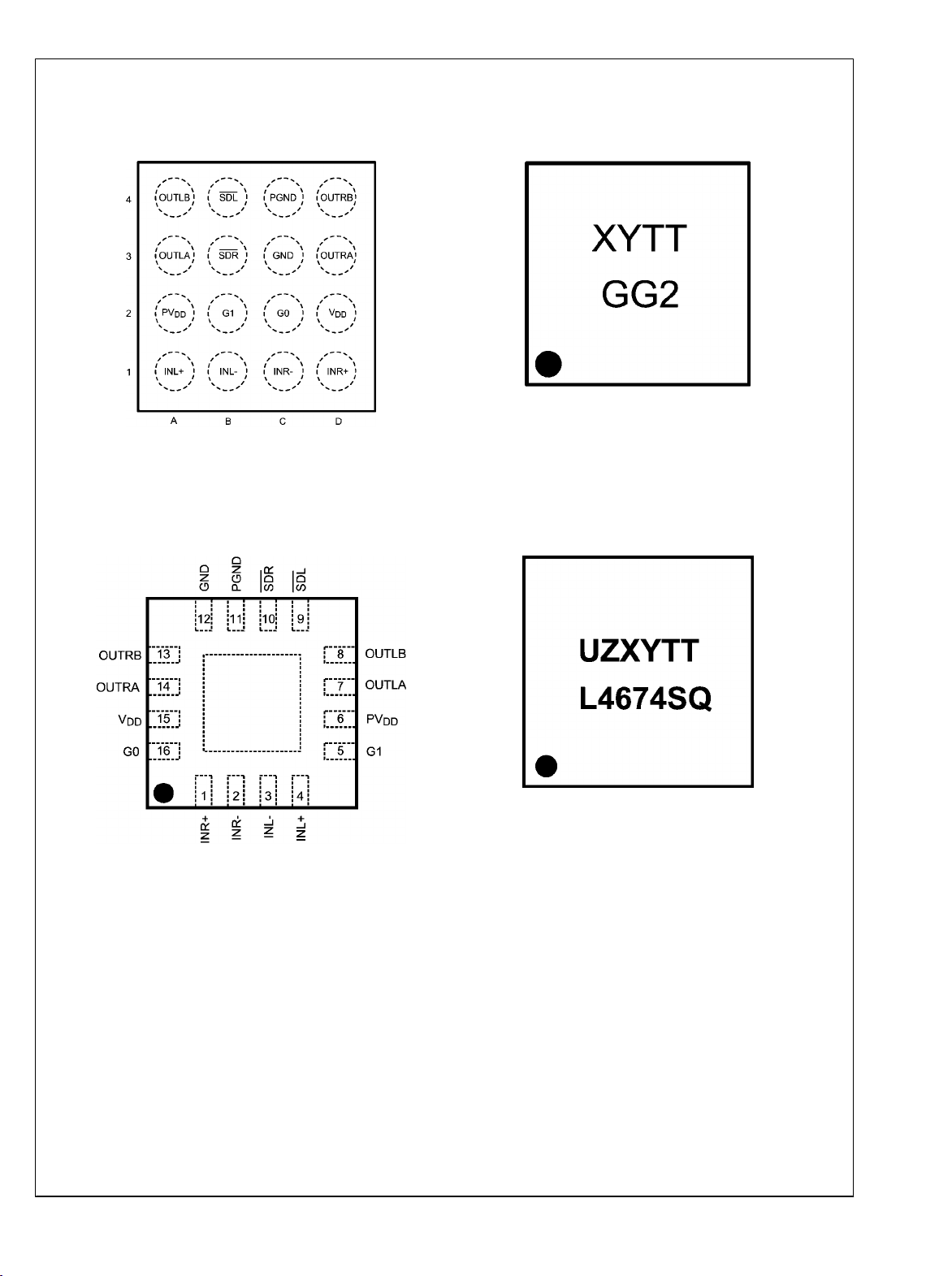
Connection Diagrams
LM4674
TL Package (2mm x 2mm x 0.6mm)
Top View
20167461
Order Number LM4674TL
See NS Package Number TL1611A
LLP Package (4mm x 4mm x 0.8mm)
LM4674TL Markings
Top View
XY = 2 Digit date code
TT = Lot traceability
G = Boomer Family
G2 = LM4674TL
LM4674SQ Markings
20167462
Order Number LM4674SQ
Top View
See NS Package Number SQA16A
20167466
Top View
20167465
U = Wafer Fab Code
Z = Assembly Plant
XY = 2 Digit date code
TT = Lot traceability
L4674SQ = LM4674SQ
3 www.national.com
LM4674
BUMP PIN NAME FUNCTION
A1 4 INL+ Non-inverting left channel input
A2 6 PV
DD
Power V
DD
A3 7 OUTLA Left channel output A
A4 8 OUTLB Left channel output B
B1 3 INL- Inverting left channel input
B2 5 G1 Gain setting input 1
B3 10 SDR Right channel shutdown input
B4 9 SDL Left channel shutdown input
C1 2 INR- Inverting right channel input
C2 16 G0 Gain setting input 0
C3 12 GND Ground
C4 11 PGND Power Ground
D1 1 INR+ Non-inverting right channel input
D2 15 V
DD
Power Supply
D3 14 OUTRA Right channel output A
D4 13 OUTRB Right channel output B
www.national.com 4
LM4674
Absolute Maximum Ratings (Notes 1, 2)
If Military/Aerospace specified devices are required,
please contact the National Semiconductor Sales Office/
Distributors for availability and specifications.
Junction Temperature (T
Thermal Resistance
θJA (μSMD)
θJA (LLP)
JMAX
)
45.7°C/W
38.9°C/W
Supply Voltage (Note 1) 6.0V
Storage Temperature −65°C to +150°C
Input Voltage –0.3V to VDD +0.3V
Power Dissipation (Note 3) Internally Limited
ESD Susceptibility, all other pins (Note 4) 2000V
ESD Susceptibility (Note 5) 200V
Operating Ratings (Notes 1, 2)
Temperature Range
T
≤ TA ≤ T
MIN
Supply Voltage
MAX
−40°C ≤ TA ≤ 85°C
2.4V ≤ VDD ≤ 5.5V
Electrical Characteristics VDD = 3.6V (Notes 1, 2)
The following specifications apply for AV = 6dB, RL = 15µH + 8Ω + 15µH, f = 1kHz unless otherwise specified. Limits apply for T
= 25°C.
Symbol Parameter Conditions
V
OS
Differential Output Offset Voltage
VIN = 0, VDD = 2.4V to 5.0V
VIN = 0, RL = ∞,
I
DD
Quiescent Power Supply Current
Both channels active, VDD = 3.6V
VIN = 0, RL = ∞,
Both channels active, VDD = 5V
I
V
V
T
SD
SDIH
SDIL
WU
Shutdown Current
Shutdown Voltage Input High 1.4 V (min)
Shutdown Voltage Input Low 0.4 V (max)
Wake Up Time V
V
SDR
SDR/SDL
= V
= GND
SDL
= 0.4V 0.5 ms
G0, G1 = GND
RL = ∞
G0 = VDD, G1 = GND
A
V
Gain
RL = ∞
G0 = GND, G1 = V
DD
RL = ∞
G0, G1 = V
DD
RL = ∞
AV = 6dB
R
IN
Input Resistance
AV = 12dB
AV = 18dB
AV = 24dB
LM4674
Typical Limit
(Note 6) (Notes 7, 8)
5 mV
4 6 mA
5 7.5 mA
0.03 1
6 6 ± 0.5 dB
12 12 ± 0.5 dB
18 18 ± 0.5 dB
24 24 ± 0.5 dB
28
18.75
11.25
6.25
Units
(Limits)
150°C
A
μA
kΩ
kΩ
kΩ
kΩ
5 www.national.com
LM4674
Symbol Parameter Conditions
LM4674
Typical Limit
(Note 6) (Notes 7, 8)
RL = 15μH + 4Ω + 15μH, THD ≤ 10%
f = 1kHz, 22kHz BW
VDD = 5V 2.5
W
VDD = 3.6V 1.2 W
VDD = 2.5V 0.530 W
RL = 15μH + 8Ω + 15μH, THD ≤ 10%
f = 1kHz, 22kHz BW
VDD = 5V
1.5 W
VDD = 3.6V 0.78 0.6 W
P
O
Output Power
VDD = 2.5V
RL = 15μH + 4Ω + 15μH, THD ≤ 1%
0.350
W
f = 1kHz, 22kHz BW
VDD = 5V
VDD = 3.6V
1.9 W
1
VDD = 2.5V 0.430 W
RL = 15μH + 8Ω + 15μH, THD = 1%
f = 1kHz, 22kHz BW
THD+N Total Harmonic Distortion
PSRR Power Supply Rejection Ratio
VDD = 5V 1.25
VDD = 3.6V
0.63
VDD = 2.5V 0.285
PO = 500mW, f = 1kHz, RL = 8Ω
PO = 300mW, f = 1kHz, RL = 8Ω
V
= 200mV
RIPPLE
f
= 217Hz, Inputs AC GND,
RIPPLE
P-P
Sine,
0.07 %
0.05 %
75
Ci = 1μF, input referred
V
= 1V
RIPPLE
f
= 1kHz, Inputs AC GND,
RIPPLE
P-P
Sine,
75
W
Ci = 1μF, input referred
V
= 1V
CMRR Common Mode Rejection Ratio
η
Efficiency
Xtalk Crosstalk
SNR Signal to Noise Ratio
ε
OS
Note 1: All voltages are measured with respect to the ground pin, unless otherwise specified.
Note 2: Absolute Maximum Ratings indicate limits beyond which damage to the device may occur. Operating Ratings indicate conditions for which the device is
functional, but do not guarantee specific performance limits. Electrical Characteristics state DC and AC electrical specifications under particular test conditions
which guarantee specific performance limits. This assumes that the device is within the Operating Ratings. Specifications are not guaranteed for parameters
where no limit is given, however, the typical value is a good indication of device performance.
Note 3: The maximum power dissipation must be derated at elevated temperatures and is dictated by T
allowable power dissipation is P
derating currents for more information.
Note 4: Human body model, 100pF discharged through a 1.5kΩ resistor.
Note 5: Machine Model, 220pF–240pF discharged through all pins.
Note 6: Typicals are measured at 25°C and represent the parametric norm.
Note 7: Limits are guaranteed to National's AOQL (Average Outgoing Quality Level).
Note 8: Datasheet min/max specification limits are guaranteed by design, test, or statistical analysis.
Output Noise
DMAX
= (T
– TA)/ θJA or the number given in Absolute Maximum Ratings, whichever is lower. For the LM4674 see power
JMAX
RIPPLE
f
RIPPLE
PO = 1W, f = 1kHz,
RL = 8Ω, VDD = 5V
PO = 500mW, f = 1kHz
VDD = 5V, PO = 1W
Input referred, A-Weighted Filter
P-P
= 217Hz
67
85
84
96
20
, θJA, and the ambient temperature, TA. The maximum
JMAX
Units
(Limits)
W
W
W
dB
dB
dB
%
dB
dB
μV
www.national.com 6
Block Diagrams
LM4674
FIGURE 2. Differential Input Configuration
20167426
7 www.national.com
LM4674
20167464
FIGURE 3. Single-Ended Input Configuration
www.national.com 8

Typical Performance Characteristics
LM4674
THD+N vs Output Power
f = 1kHz, AV = 24dB, RL = 8Ω
THD+N vs Output Power
f= 1kHz, AV = 24dB, RL = 4Ω
20167439
THD+N vs Output Power
f = 1kHz, AV = 6dB, RL = 8Ω
20167440
THD+N vs Output Power
f = 1kHz, AV = 6dB, RL = 4Ω
VDD = 2.5V, P
THD+N vs Frequency
= 100mW/ch, RL = 8Ω
OUT
20167441
20167443
20167442
THD+N vs Frequency
VDD = 3.6V, P
9 www.national.com
= 250mW/ch, RL = 8Ω
OUT
20167444

LM4674
THD+N vs Frequency
VDD = 5V, P
OUT
= 375mW/ch, RL = 8Ω
VDD = 2.5V, P
THD+N vs Frequency
= 100mW/ch, RL = 4Ω
OUT
VDD = 3.6V, P
= 250mW/ch, RL = 4Ω
OUT
Efficiency vs Output Power/channel
RL = 4Ω, f = 1kHz
THD+N vs Frequency
20167445
20167447
THD+N vs Frequency
VDD = 5V, P
= 375mW/ch, RL = 4Ω
OUT
Efficiency vs Output Power/channel
RL = 8Ω, f = 1kHz
20167446
20167448
20167449
www.national.com 10
20167450

LM4674
Power Dissipation vs Output Power
RL = 4Ω, f = 1kHz
20167451
Output Power/channel vs Supply Voltage
RL = 4Ω, f = 1kHz
Power Dissipation vs Output Power
RL = 8Ω, f = 1kHz
20167452
Output Power/channel vs Supply Voltage
RL = 8Ω, f = 1kHz
VDD = 3.6V, V
PSRR vs Frequency
RIPPLE
= 200mV
, RL = 8Ω
P-P
20167453
20167455
20167454
Crosstalk vs Frequency
VDD = 3.6V, V
11 www.national.com
RIPPLE
= 1V
, RL = 8Ω
P-P
20167422

LM4674
CMRR vs Frequency
VDD = 3.6V, VCM = 1V
, RL = 8Ω
P-P
Supply Current vs Supply Voltage
RL = ∞
20167457
20167458
www.national.com 12

Application Information
GENERAL AMPLIFIER FUNCTION
The LM4674 stereo Class D audio power amplifier features a
filterless modulation scheme that reduces external component count, conserving board space and reducing system
cost. The outputs of the device transition from VDD to GND
with a 300kHz switching frequency. With no signal applied,
the outputs for each channel switch with a 50% duty cycle, in
phase, causing the two outputs to cancel. This cancellation
results in no net voltage across the speaker, thus there is no
current to the load in the idle state.
With the input signal applied, the duty cycle (pulse width) of
the LM4674 outputs changes. For increasing output voltage,
the duty cycle of the A output increases, while the duty cycle
of the B output decreases for each channel. For decreasing
output voltages, the converse occurs. The difference between
the two pulse widths yields the differential output voltage.
DIFFERENTIAL AMPLIFIER EXPLANATION
As logic supplies continue to shrink, system designers are increasingly turning to differential analog signal handling to
preserve signal to noise ratios with restricted voltage signs.
The LM4674 features two fully differential amplifiers. A differential amplifier amplifies the difference between the two input
signals. Traditional audio power amplifiers have typically offered only single-ended inputs resulting in a 6dB reduction of
SNR relative to differential inputs. The LM4674 also offers the
possibility of DC input coupling which eliminates the input
coupling capacitors. A major benefit of the fully differential
amplifier is the improved common mode rejection ratio (CMRR) over single ended input amplifiers. The increased CMRR
of the differential amplifier reduces sensitivity to ground offset
related noise injection, especially important in noisy systems.
POWER DISSIPATION AND EFFICIENCY
The major benefit of a Class D amplifier is increased efficiency
versus a class AB amplifier. The efficiency of the LM4674 is
attributed to the region of operation of the transistors in the
output stage. The Class D output stage acts as current steering switches, consuming negligible amounts of power compared to their Class AB counterparts. Most of the power loss
associated with the output stage is due to the IR loss of the
MOSFET on-resistance (R
due to gate charge.
SHUTDOWN FUNCTION
The LM4674 features independent left and right channel shutdown controls, allowing each channel to be disabled independently. SDR controls the right channel, while SDL controls
the left channel. Driving either low disables the corresponding
channel.
It is best to switch between ground and VDD for minimum current consumption while in shutdown. The LM4674 may be
disabled with shutdown voltages in between GND and VDD,
the idle current will be greater than the typical 0.03µA value.
For logic levels between GND and VDD bypass SD_ with a
0.1μF capacitor.
The LM4674 shutdown inputs have internal pulldown resis-
tors. The purpose of these resistors is to eliminate any un-
), along with switching losses
DS(ON)
wanted state changes when SD_ is floating. To minimize
shutdown current, SD_ should be driven to GND or left floating. If SD_ is not driven to GND or floating, an increase in
shutdown supply current will be noticed.
SINGLE-ENDED AUDIO AMPLIFIER CONFIGURATION
The LM4674 is compatible with single-ended sources. When
configured for single-ended inputs, input capacitors must be
used to block any DC component at the input of the device.
Figure 3 shows the typical single-ended applications circuit.
AUDIO AMPLIFIER POWER SUPPLY BYPASSING/ FILTERING
Proper power supply bypassing is critical for low noise performance and high PSRR. Place the supply bypass capacitor
as close to the device as possible. Typical applications employ a voltage regulator with 10µF and 0.1µF bypass capacitors that increase supply stability. These capacitors do not
eliminate the need for bypassing of the LM4674 supply pins.
A 1µF capacitor is recommended.
AUDIO AMPLIFIER INPUT CAPACITOR SELECTION
Input capacitors may be required for some applications, or
when the audio source is single-ended. Input capacitors block
the DC component of the audio signal, eliminating any conflict
between the DC component of the audio source and the bias
voltage of the LM4674. The input capacitors create a highpass filter with the input resistance Ri. The -3dB point of the
high pass filter is found using Equation 1 below.
f = 1 / 2πRiC
The values for Ri can be found in the EC table for each gain
setting.
The input capacitors can also be used to remove low frequency content from the audio signal. Small speakers cannot
reproduce, and may even be damaged by low frequencies.
High pass filtering the audio signal helps protect the speakers.
When the LM4674 is using a single-ended source, power
supply noise on the ground is seen as an input signal. Setting
the high-pass filter point above the power supply noise frequencies, 217 Hz in a GSM phone, for example, filters out the
noise such that it is not amplified and heard on the output.
Capacitors with a tolerance of 10% or better are recommended for impedance matching and improved CMRR and PSRR.
AUDIO AMPLIFIER GAIN SETTING
The LM4674 features four internally configured gain settings.
The device gain is selected through the two logic inputs, G0
and G1. The gain settings are as shown in the following table.
LOGIC INPUT GAIN
G1 G0 V/V dB
0 0 2 6
0 1 4 12
1 0 8 18
1 1 16 24
i
(1)
LM4674
13 www.national.com

PCB LAYOUT GUIDELINES
As output power increases, interconnect resistance (PCB
LM4674
traces and wires) between the amplifier, load and power supply create a voltage drop. The voltage loss due to the traces
between the LM4674 and the load results in lower output
power and decreased efficiency. Higher trace resistance between the supply and the LM4674 has the same effect as a
poorly regulated supply, increasing ripple on the supply line,
and reducing peak output power. The effects of residual trace
resistance increases as output current increases due to higher output power, decreased load impedance or both. To maintain the highest output voltage swing and corresponding peak
output power, the PCB traces that connect the output pins to
the load and the supply pins to the power supply should be
as wide as possible to minimize trace resistance.
The use of power and ground planes will give the best THD
+N performance. In addition to reducing trace resistance, the
use of power planes creates parasitic capacitors that help to
filter the power supply line.
The inductive nature of the transducer load can also result in
overshoot on one or both edges, clamped by the parasitic
diodes to GND and VDD in each case. From an EMI standpoint, this is an aggressive waveform that can radiate or
conduct to other components in the system and cause interference. In is essential to keep the power and output traces
short and well shielded if possible. Use of ground planes
beads and micros-strip layout techniques are all useful in preventing unwanted interference.
As the distance from the LM4674 and the speaker increases,
the amount of EMI radiation increases due to the output wires
or traces acting as antennas become more efficient with
length. Ferrite chip inductors places close to the LM4674 outputs may be needed to reduce EMI radiation.
www.national.com 14

LM4674TL Demo Board Schematic
LM4674
LM4674TL Demo Board Schematic
20167474
15 www.national.com

LM4674TL Demonstration Board Layout
LM4674
Layer 1
Layer 2
20167476
20167477
Layer 3
www.national.com 16
20167478

LM4674
Layer 4
Top Silkscreen
20167479
20167480
Bottom Silkscreen
17 www.national.com
20167475

LM4674SQ Demo Board Schematic
LM4674
LM4674SQ Demo Board Schematic
20167481
www.national.com 18

LM4674SQ Demonstration Board Layout
LM4674
Layer 1
Layer 2
20167485
20167483
Layer 3
19 www.national.com
20167484

LM4674
Top Silkscreen
Bottom Layer
20167486
20167487
www.national.com 20

Revision Table
Rev Date Description
1.0 12/16/06 Initial release.
1.1 05/17/06 Added the LLP package.
1.2 05/31/06 Added the LLP markings.
1.3 09/05/06 Added “No Load” in the Conditions on Av (3.6V table).
1.4 09/21/06 Edited graphics (26, 38, 60) and input some text edits.
1.5 09/27/06 Edited Figure 1 (page 2), TL and LLP pkg/marking drawings (page 3).
1.6 07/13/07 Added the TL and SQ demo boards and schematics diagrams.
1.7 10/30/07 Updated the SQ schematic diagram and replaced the demo boards.
1.8 07/02/08 Text edits (under SHUTDOWN FUNCTION).
LM4674
Input text edits.
21 www.national.com

Physical Dimensions inches (millimeters) unless otherwise noted
LM4674
16 Bump micro SMD
Order Number LM4674TL
NS Package Number TLA1611A
X1 = 2mm X2 = 2mm X3 = 0.6mm
LLP Package
Order Number LM4674SQ
NS Package Number SQA16A
www.national.com 22

Notes
LM4674
23 www.national.com

Notes
For more National Semiconductor product information and proven design tools, visit the following Web sites at:
Products Design Support
Amplifiers www.national.com/amplifiers WEBENCH www.national.com/webench
Audio www.national.com/audio Analog University www.national.com/AU
Clock Conditioners www.national.com/timing App Notes www.national.com/appnotes
Data Converters www.national.com/adc Distributors www.national.com/contacts
Displays www.national.com/displays Green Compliance www.national.com/quality/green
Ethernet www.national.com/ethernet Packaging www.national.com/packaging
Interface www.national.com/interface Quality and Reliability www.national.com/quality
LVDS www.national.com/lvds Reference Designs www.national.com/refdesigns
Power Management www.national.com/power Feedback www.national.com/feedback
Switching Regulators www.national.com/switchers
LDOs www.national.com/ldo
LED Lighting www.national.com/led
PowerWise www.national.com/powerwise
Serial Digital Interface (SDI) www.national.com/sdi
Temperature Sensors www.national.com/tempsensors
Wireless (PLL/VCO) www.national.com/wireless
THE CONTENTS OF THIS DOCUMENT ARE PROVIDED IN CONNECTION WITH NATIONAL SEMICONDUCTOR CORPORATION
(“NATIONAL”) PRODUCTS. NATIONAL MAKES NO REPRESENTATIONS OR WARRANTIES WITH RESPECT TO THE ACCURACY
OR COMPLETENESS OF THE CONTENTS OF THIS PUBLICATION AND RESERVES THE RIGHT TO MAKE CHANGES TO
SPECIFICATIONS AND PRODUCT DESCRIPTIONS AT ANY TIME WITHOUT NOTICE. NO LICENSE, WHETHER EXPRESS,
IMPLIED, ARISING BY ESTOPPEL OR OTHERWISE, TO ANY INTELLECTUAL PROPERTY RIGHTS IS GRANTED BY THIS
DOCUMENT.
TESTING AND OTHER QUALITY CONTROLS ARE USED TO THE EXTENT NATIONAL DEEMS NECESSARY TO SUPPORT
NATIONAL’S PRODUCT WARRANTY. EXCEPT WHERE MANDATED BY GOVERNMENT REQUIREMENTS, TESTING OF ALL
PARAMETERS OF EACH PRODUCT IS NOT NECESSARILY PERFORMED. NATIONAL ASSUMES NO LIABILITY FOR
APPLICATIONS ASSISTANCE OR BUYER PRODUCT DESIGN. BUYERS ARE RESPONSIBLE FOR THEIR PRODUCTS AND
APPLICATIONS USING NATIONAL COMPONENTS. PRIOR TO USING OR DISTRIBUTING ANY PRODUCTS THAT INCLUDE
NATIONAL COMPONENTS, BUYERS SHOULD PROVIDE ADEQUATE DESIGN, TESTING AND OPERATING SAFEGUARDS.
LM4674 Filterless 2.5W Stereo Class D Audio Power Amplifier
EXCEPT AS PROVIDED IN NATIONAL’S TERMS AND CONDITIONS OF SALE FOR SUCH PRODUCTS, NATIONAL ASSUMES NO
LIABILITY WHATSOEVER, AND NATIONAL DISCLAIMS ANY EXPRESS OR IMPLIED WARRANTY RELATING TO THE SALE
AND/OR USE OF NATIONAL PRODUCTS INCLUDING LIABILITY OR WARRANTIES RELATING TO FITNESS FOR A PARTICULAR
PURPOSE, MERCHANTABILITY, OR INFRINGEMENT OF ANY PATENT, COPYRIGHT OR OTHER INTELLECTUAL PROPERTY
RIGHT.
LIFE SUPPORT POLICY
NATIONAL’S PRODUCTS ARE NOT AUTHORIZED FOR USE AS CRITICAL COMPONENTS IN LIFE SUPPORT DEVICES OR
SYSTEMS WITHOUT THE EXPRESS PRIOR WRITTEN APPROVAL OF THE CHIEF EXECUTIVE OFFICER AND GENERAL
COUNSEL OF NATIONAL SEMICONDUCTOR CORPORATION. As used herein:
Life support devices or systems are devices which (a) are intended for surgical implant into the body, or (b) support or sustain life and
whose failure to perform when properly used in accordance with instructions for use provided in the labeling can be reasonably expected
to result in a significant injury to the user. A critical component is any component in a life support device or system whose failure to perform
can be reasonably expected to cause the failure of the life support device or system or to affect its safety or effectiveness.
National Semiconductor and the National Semiconductor logo are registered trademarks of National Semiconductor Corporation. All other
brand or product names may be trademarks or registered trademarks of their respective holders.
Copyright© 2008 National Semiconductor Corporation
For the most current product information visit us at www.national.com
www.national.com
National Semiconductor
Americas Technical
Support Center
Email: support@nsc.com
Tel: 1-800-272-9959
National Semiconductor Europe
Technical Support Center
Email: europe.support@nsc.com
German Tel: +49 (0) 180 5010 771
English Tel: +44 (0) 870 850 4288
National Semiconductor Asia
Pacific Technical Support Center
Email: ap.support@nsc.com
National Semiconductor Japan
Technical Support Center
Email: jpn.feedback@nsc.com
 Loading...