


September 2006
LM4550B
AC ’97 Rev 2.1 Multi-Channel Audio Codec with Stereo
Headphone Amplifier, Sample Rate Conversion and
National 3D Sound
LM4550B AC ’97 Rev 2.1 Multi-Channel Audio Codec with Stereo Headphone Amplifier, Sample
Rate Conversion and National 3D Sound
General Description
The LM4550B is an audio codec for PC systems which is
fully PC99 compliant and performs the analog intensive
functions of the AC ’97 Rev 2.1 architecture. Using 18-bit
Sigma-Delta ADCs and DACs, the LM4550B provides 90 dB
of Dynamic Range.
The LM4550B was designed specifically to provide a high
quality audio path and provide all analog functionality in a PC
audio system. It features full duplex stereo ADCs and DACs
and analog mixers with access to 4 stereo and 4 mono
inputs. Each mixer input has separate gain, attenuation and
mute control and the mixers drive 1 mono and 2 stereo
outputs, each with attenuation and mute control. The
LM4550B provides a stereo headphone amplifier as one of
its stereo outputs and also supports National’s 3D Sound
stereo enhancement and a comprehensive sample rate conversion capability. The sample rate for the ADCs and DACs
can be programmed separately with a resolution of 1 Hz to
convert any rate in the range 4 kHz – 48 kHz. Sample timing
from the ADCs and sample request timing for the DACs are
completely deterministic to ease task scheduling and application software development. These features together with
an extended temperature range also make the LM4550B
suitable for non-PC codec applications.
The LM4550B features the ability to connect several codecs
together in a system to provide up to 6 simultaneous channels of streaming data on Output Frames (Controller to
Codec) for surround sound applications. Such systems can
also support up to 8 simultaneous channels of streaming
data on Input Frames (Codec to Controller). Multiple codec
systems can be built either using the standard AC Link
configuration (i.e. of one serial data signal to the Controller
per codec) or using a unique National Semiconductor feature for chaining codecs together. This chain feature shares
only a single data signal to the controller among multiple
codecs.
The AC ’97 architecture separates the analog and digital
functions of the PC audio system allowing both for system
design flexibility and increased performance.
Key Specifications
n Analog Mixer Dynamic Range 97 dB (typ)
n DAC Dynamic Range 89 dB (typ)
n ADC Dynamic Range 90 dB (typ)
n Headphone Amp THD+N at 50 mW 0.02% (typ)
into 32Ω
Features
n AC ’97 Rev 2.1 compliant
n High quality Sample Rate Conversion from 4 kHz to 48
kHz in 1 Hz increments
n Supports up to 6 DAC channel systems with multiple
LM4550Bs or with other National LM45xx codecs
n Unique National chaining function shares a single
controller SDATA_IN pin among multiple codecs
n Stereo headphone amp with separate gain control
n National’s 3D Sound stereo enhancement circuitry
n Advanced power management support
n External Amplifier Power Down (EAPD) control
n PC Beep passthrough to Line Out during Initialization or
Cold Reset
n Digital 3.3V and 5V supply options
n Extended Temperature: −40˚C ≤ T
≤ 85˚C
A
Applications
n Desktop PC audio systems on PCI cards, AMR cards, or
with motherboard chips sets featuring AC Link
n Portable PC systems as on MDC cards, or with a
chipset or accelerator featuring AC Link
n General Audio Frequency Systems requiring 2, 4 or 6
DAC channels and/or up to 8 ADC channels
n Automotive telematics
© 2006 National Semiconductor Corporation DS201237 www.national.com
LM4550B
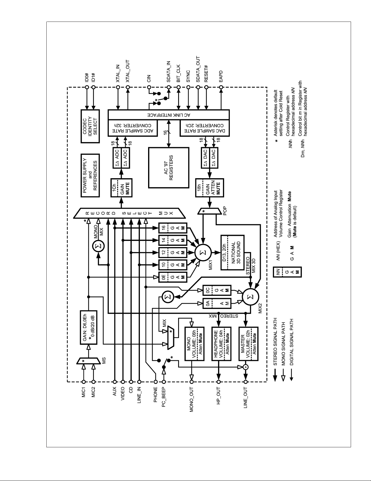
20123701
Block Diagram
www.national.com 2
LM4550B
Absolute Maximum Ratings (Note 1)
If Military/Aerospace specified devices are required,
please contact the National Semiconductor Sales Office/
Distributors for availability and specifications.
Supply Voltage 6.0V
Soldering Information
LQFP Package
Vapor Phase (60 sec.) 215˚C
Infrared (15 sec.) 220˚C
θ
(typ) – VBH48A 74˚C/W
JA
Storage Temperature −65˚C to +150˚C
Input Voltage −0.3V to V
DD
+0.3V
Operating Ratings
ESD Susceptibility (Note 2) 2000V
pin 3 750
ESD Susceptibility (Note 3) 200V
pin 3 100V
Junction Temperature 150˚C
Electrical Characteristics (Notes 1, 5) The following specifications apply for AV
48 kHz, single codec configuration, (primary mode) unless otherwise noted. Limits apply for T
Temperature Range
T
MIN
≤ TA≤ T
(Note 4) −40˚C ≤ TA≤ 85˚C
MAX
Analog Supply Range 4.2V ≤ AV
Digital Supply Range 3.0V ≤ DV
= 5V, DVDD= 3.3V, Fs =
DD
= 25˚C. The reference for 0 dB
A
DD
DD
≤ 5.5V
≤ 5.5V
is 1 Vrms unless otherwise specified.
Units
(Limits)
Symbol Parameter Conditions
AV
DD
Analog Supply Range 4.2 V (min)
LM4550B
Typical
(Note 6)
Limit
(Note 7)
5.5 V (max)
DV
DD
Digital Supply Range 3.0 V (min)
5.5 V (max)
= 5 V 34 mA
D
A
I
I
V
DSD
ASD
IDD
IDD
REF
Digital Quiescent Power Supply
Current
Analog Quiescent Power Supply
Current
Digital Shutdown Current PR6543210 = 1111111 19 µA
Analog Shutdown Current PR6543210 = 1111111 70 µA
Reference Voltage No pullup resistor 2.16 V
DV
DD
DV
= 3.3 V 19 mA
DD
= 5 V 53 mA
AV
DD
PSRR Power Supply Rejection Ratio 40 dB
Analog Loopthrough Mode (Note 8)
Dynamic Range (Note 9)
THD Total Harmonic Distortion V
CD Input to Line Output, -60 dB Input
THD+N
=-3dB,f=1kHz, RL=10kΩ 0.013 0.02 % (max)
O
97 90 dB (min)
Analog Input Section
V
IN
V
IN
V
IN
Line Input Voltage
Mic Input with 20 dB Gain 0.1 Vrms
Mic Input with 0 dB Gain 1 Vrms
LINE_IN, AUX, CD, VIDEO, PC_BEEP,
PHONE
1 Vrms
Xtalk Crosstalk CD Left to Right −95 dB
Z
IN
C
IN
Input Impedance (Note 9) All Analog Inputs 40 10 kΩ (min)
Input Capacitance(Note 9) 3.7 7 pF
Interchannel Gain Mismatch CD Left to Right 0.10 dB
Record Gain Amplifier - ADC
A
S
A
M
Step Size 0 dB to 22.5 dB 1.5 dB
Mute Attenuation (Note 9) 86 dB
Mixer Section
A
S
A
M
Step Size +12 dB to -34.5 dB 1.5 dB
Mute Attenuation(Note 9) 86 dB
www.national.com3
Electrical Characteristics (Notes 1, 5) The following specifications apply for AV
48 kHz, single codec configuration, (primary mode) unless otherwise noted. Limits apply for T
is 1 Vrms unless otherwise specified. (Continued)
LM4550B
= 5V, DVDD= 3.3V, Fs =
DD
= 25˚C. The reference for 0 dB
A
Units
(Limits)
Symbol Parameter Conditions
LM4550B
Typical
(Note 6)
Limit
(Note 7)
Analog to Digital Converters
Resolution 18 Bits
Dynamic Range (Note 9) -60 dB Input THD+N, A-Weighted 90 86 dB (min)
Frequency Response -1 dB Bandwidth 20 kHz
Digital to Analog Converters
Resolution 18 Bits
Dynamic Range (Note 9) -60 dB Input THD+N, A-Weighted 89 82 dB (min)
THD Total Harmonic Distortion V
=-3dB,f=1kHz, RL=10kΩ 0.01 %
IN
Frequency Response 20-21 k Hz
Group Delay (Note 9) Sample Freq. = 48 kHz 0.36 1
ms
(max)
Out of Band Energy (Note 10) -40 dB
Stop Band Rejection 70 dB
D
T
Discrete Tones -96 dB
Analog Output Section
A
S
A
M
THD+N
Z
OUT
Z
OUT
Step Size 0 dB to -46.5 dB 1.5 dB
Mute Attenuation(Note 9) 86 dB
Headphone Amplifier Total
Harmonic Distortion plus Noise
Loopthrough Mode (Note 8), R
f = 1 kHz, P
=50mW
out
=32Ω,
L
0.02 %
Output Impedance (Note 9) HP_OUT_L, HP_OUT_R 0.65 2.75 Ω
Output Impedance (Note 9)
LINE_OUT_L, LINE_OUT_R,
MONO_OUT
220 500 Ω
Digital I/O (Note 9)
V
IH
V
IL
V
OH
V
OL
I
L
I
L
High level input voltage
Low level input voltage
High level output voltage IO= −2.5 mA.
Low level output voltage IO= 2.5 mA.
Input Leakage Current AC Link inputs
Tri state Leakage Current High impedance AC Link outputs
0.65 x
DV
DD
0.35 x
DV
DD
0.90 x
DV
DD
0.10 x
DV
DD
±
10 µA
±
10 µA
V (min)
V (max)
V (min)
V (max)
Cin AC-Link I/O capacitance SDout, BitClk, SDin, Sync, Reset# only 4 7.5 pF (max)
I
DR
Output drive current AC Link outputs 5 mA
Digital Timing Specifications (Note 9)
F
BC
T
BCP
T
CH
F
SYNC
T
SP
T
SH
T
SL
T
DSETUP
BIT_CLK frequency 12.288 MHz
BIT_CLK period 81.4 ns
BIT_CLK high
Variation of BIT_CLK duty cycle from
50%
±
20 % (max)
SYNC frequency 48 kHz
SYNC period 20.8 µs
SYNC high pulse width 1.3 µs
SYNC low pulse width 19.5 µs
Setup Time for codec data input SDATA_OUT to falling edge of BIT_CLK 3.5 10 ns (min)
www.national.com 4
LM4550B
Electrical Characteristics (Notes 1, 5) The following specifications apply for AV
48 kHz, single codec configuration, (primary mode) unless otherwise noted. Limits apply for T
= 5V, DVDD= 3.3V, Fs =
DD
= 25˚C. The reference for 0 dB
A
is 1 Vrms unless otherwise specified. (Continued)
JMAX
Units
(Limits)
ns (max)
= 150˚C.
Symbol Parameter Conditions
T
DHOLD
T
SSETUP
T
SHOLD
T
CO
T
RISE
T
FALL
T
CS
T
RST_LOW
T
RST2CLK
T
SH
T
SYNC2CLK
T
S2_PDOWN
T
SUPPLY2RST
T
SU2RST
T
RST2HZ
Note 1: Absolute Maximum Ratings indicate limits beyond which damage to the device may occur. Operating Ratings indicate conditions for which the device is
functional, but do not guarantee specific performance limits. Electrical Characteristics state DC andAC electrical specifications under particular test conditions which
guarantee specific performance limits. This assumes that the device is within the Operating Ratings. Specifications are not guaranteed for parameters where no limit
is given, however, the typical value is a good indication of device performance.
Note 2: Human body model, 100 pF discharged through a 1.5 kΩ resistor.
Note 3: Machine Model, 220 pF – 240 pF discharged through all pins.
Note 4: The maximum power dissipation must be derated at elevated temperatures and is dictated by T
allowable power dissipation is P
The typical junction-to-ambient thermal resistance is 74˚C/W for package number VBH48A.
Note 5: All voltages are measured with respect to the ground pin, unless otherwise specified.
Note 6: Typicals are measured at 25˚C and represent the parametric norm.
Note 7: Limits are guaranteed to National’s AOQL (Average Outgoing Quality Level).
Note 8: Loopthrough Mode describes a path from an analog input through the analog mixers to an analog output.
Note 9: These specifications are guaranteed by design and characterization; they are not production tested.
Note 10: Out of band energy is measured from 28.8 kHz to 100 kHz relative toa1VrmsDACoutput.
Hold Time for codec data input
Setup Time for codec SYNC input
Hold Time for codec SYNC input
Output Valid Delay
Rise Time
Fall Time
Chain Propagation Delay
RESET# active low pulse width For Cold Reset 1.0 µs (min)
RESET# inactive to BIT_CLK start
up
SYNC active high pulse width For Warm Reset 1.0 µs (min)
SYNC inactive to BIT_CLK start up For Warm Reset 162.8 ns (min)
AC Link Power Down Delay
Power On Reset
Setup to trailing edge of RESET# For ATE Test Mode 15 ns (min)
Rising edge of RESET# to Hi-Z For ATE Test Mode 25 ns (max)
DMAX
=(T
)/θJAor the number given in Absolute Maximum Ratings, whichever is lower. For the LM4550B, T
JMAX–TA
Hold time of SDATA_OUT from falling
edge of BIT_CLK (Note 9)
SYNC to falling edge of BIT_CLK (Note
9)
Hold time of SYNC from falling edge of
BIT_CLK
Output Delay of SDATA_IN from rising
edge of BIT_CLK (Note 9)
BIT_CLK, SYNC, SDATA_IN or
SDATA_OUT
BIT_CLK, SYNC, SDATA_IN or
SDATA_OUT
Data Delay from CIN to SDATA_IN
when the chain feature is active
For Cold Reset 271 162.8 ns (min)
Delay from end of Slot 2 to BIT_CLK,
SDATA_IN low
Time from minimum valid supply levels
to end of Reset
, θJA, and the ambient temperature TA. The maximum
JMAX
LM4550B
Typical
(Note 6)
Limit
(Note 7)
5.3 10 ns (min)
3.8 10 ns (min)
10 ns (min)
5.2 15 ns (max)
6 ns (max)
6 ns (max)
1 µs (max)
1 µs (min)
www.national.com5
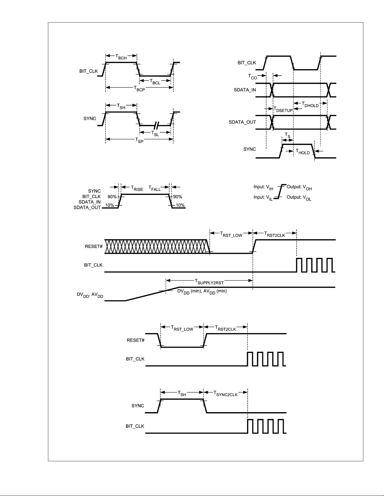
Timing Diagrams
LM4550B
Clocks Data Delay, Setup and Hold
20123710
20123711
Digital Rise and Fall Legend
20123730
20123712
Power On Reset
Cold Reset
Warm Reset
www.national.com 6
20123729
20123713
20123714
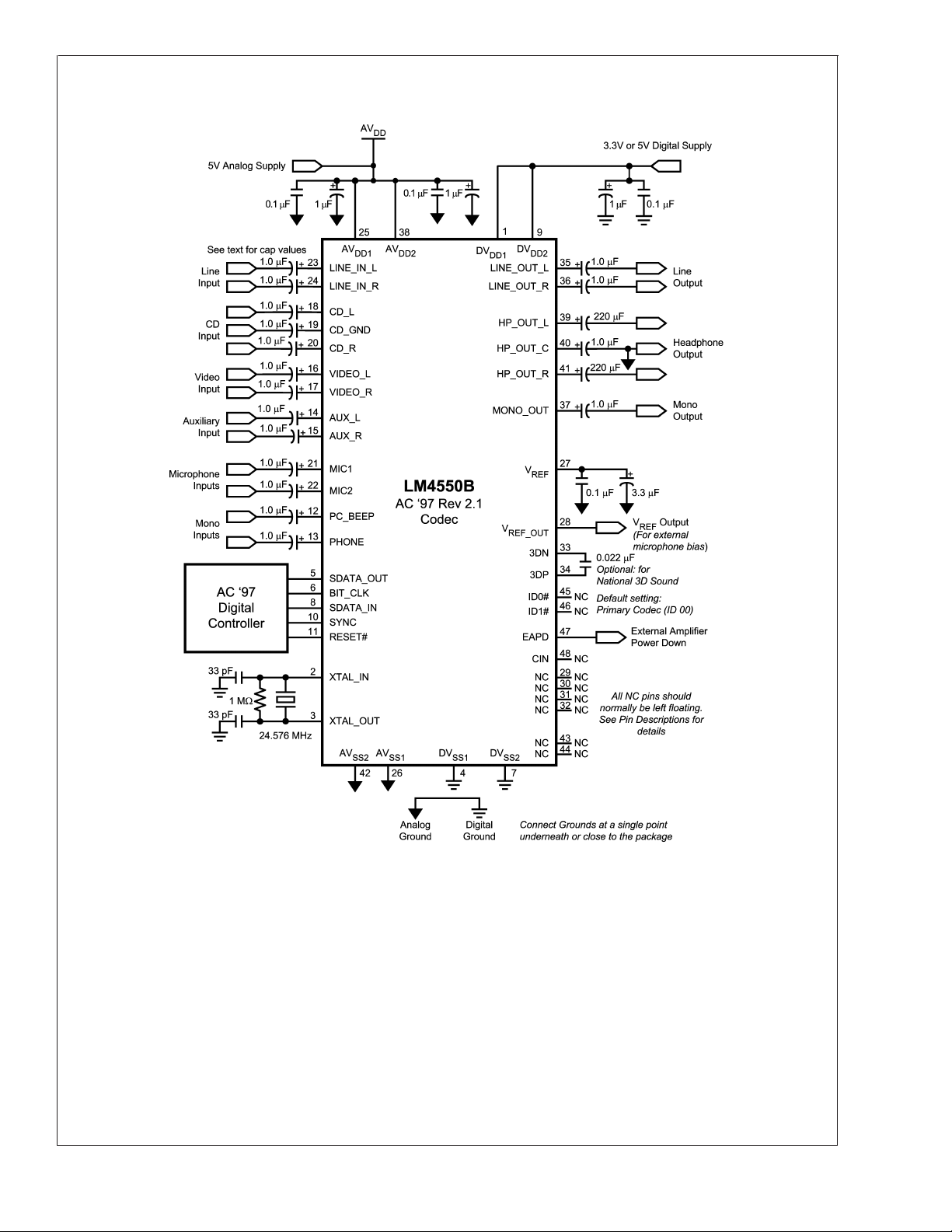
Typical Application
LM4550B
20123703
FIGURE 1. LM4550B Typical Application Circuit, Single Codec, 1 Vrms inputs
APPLICATION HINTS
The LM4550B must be initialized by using RESET# to perform a Power On Reset as shown in the Power On Reset Timing
•
Diagram
Don’t leave unused Analog inputs floating. Tie all unused inputs together and connect to Analog Ground through a capacitor
•
(e.g. 0.1 µF)
Do not leave CD_GND floating when using the CD stereo input. CD_GND is the AC signal reference for the CD channels and
•
should be connected to the CD source ground (Analog Ground may also be acceptable) througha1µFcapacitor
If using a non-standard AC Link controller take care to keep the SYNC and SDATA_OUT signals low during Cold Reset to
•
avoid accidentally activating the ATE or Vendor test modes
The PC_Beep input should be explicitly muted if not used since it defaults to 0 dB gain on reset, unlike the mute default of the
•
other analog inputs
www.national.com7
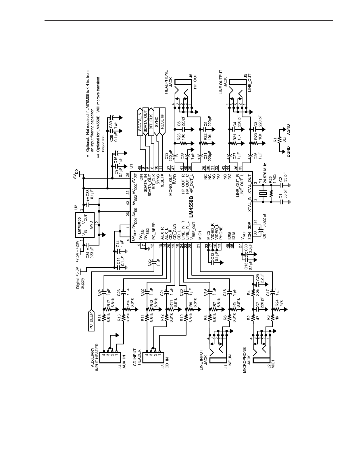
LM4550B
20123725
Typical Application (Continued)
www.national.com 8
FIGURE 2. LM4550B Reference Design, Typical Application, Single Codec, 1 Vrms and 2 Vrms inputs, EMC output filters
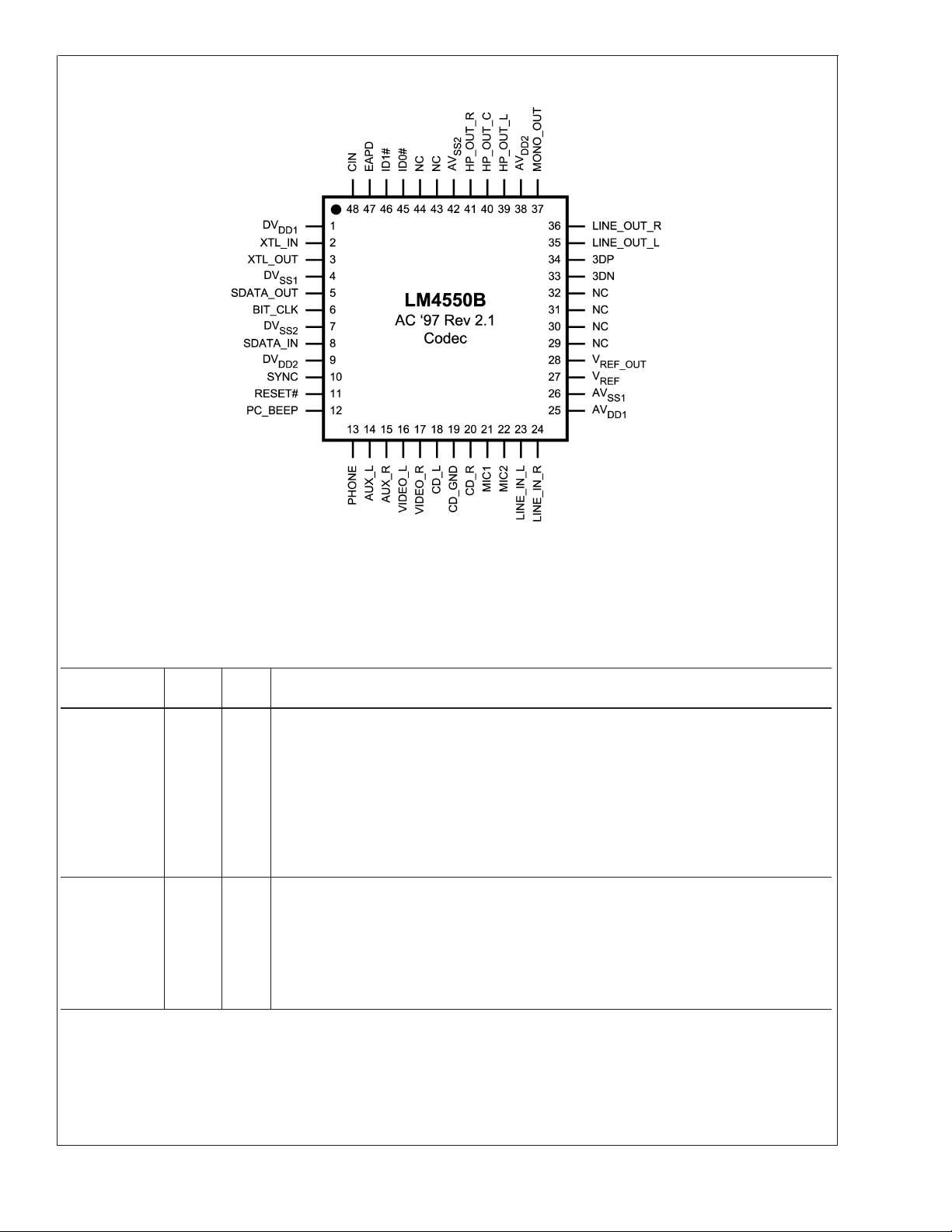
Connection Diagram
LM4550B
Pin Descriptions
Name Pin I / O
PC_BEEP 12 I
PHONE 13 I
Top View
20123702
Order Number LM4550BVH
See NS Package Number VBH48A
ANALOG I/O
Functional Description
Mono Input
This line level (1 Vrms nominal) mono input is mixed equally into both channels of the Stereo
Mix signal at MIX2 under the control of the PC_Beep Volume control register, 0Ah. The
PC_BEEP level can be muted or adjusted from 0 dB to -45 dB in 3 dB steps. The Stereo Mix
signal feeds both the Line Out and Headphone Out analog outputs and is also selectable at
the Record Select Mux. During Initialization or Cold Reset, (reset pin held active low),
PC_BEEP is switched directly to both channels of the Line Out stereo output, bypassing all
volume controls. This allows signals such as PC power-on self-test tones to be heard through
the PC’s audio system before the codec registers are configured.
Mono Input
This line level (1 Vrms nominal) mono input is selectable at the Record Select Mux for
conversion by either or both channels of the stereo ADC. It can also be mixed equally into
both channels of the Stereo Mix signal at MIX2 under the control of the Phone Volume
register, 0Ch. The PHONE level can be muted or adjusted from +12 dB to -34.5 dB in 1.5 dB
steps. The Stereo Mix signal feeds both the Line Out and Headphone Out analog stereo
outputs and is also selectable at the Record Select Mux.
www.national.com9

Pin Descriptions (Continued)
LM4550B
Name Pin I / O
AUX_L 14 I
AUX_R 15 I
VIDEO_L 16 I
VIDEO_R 17 I
CD_L 18 I
CD_GND 19 I
CD_R 20 I
ANALOG I/O (Continued)
Functional Description
Left Stereo Channel Input
This line level input (1 Vrms nominal) is selectable at the left channel of the stereo Record
Select Mux for conversion by the left channel ADC. It can also be mixed into the left channel
of the Stereo Mix 3D signal at MIX1 under the control of the Aux Volume register, 16h. The
AUX_L level can be muted (along with AUX_R) or adjusted from +12 dB to -34.5 dB in 1.5 dB
steps. Stereo Mix 3D is combined into the Stereo Mix signal at MIX2 for access to the stereo
outputs Line Out and Headphone Out.
Right Stereo Channel Input
This line level input (1 Vrms nominal) is selectable at the right channel of the stereo Record
Select Mux for conversion by the right channel ADC. It can also be mixed into the right
channel of the Stereo Mix 3D signal at MIX1 under the control of the Aux Volume register,
16h. The AUX_R level can be muted (along with AUX_L) or adjusted from +12 dB to -34.5 dB
in 1.5 dB steps. Stereo Mix 3D is combined into the Stereo Mix signal at MIX2 for access to
the stereo outputs Line Out and Headphone Out.
Left Stereo Channel Input
This line level input (1 Vrms nominal) is selectable at the left channel of the stereo Record
Select Mux for conversion by the left channel ADC. It can also be mixed into the left channel
of the Stereo Mix 3D signal at MIX1 under the control of the Video Volume register, 14h. The
VIDEO_L level can be muted (along with VIDEO_R) or adjusted from +12 dB to -34.5 dB in
1.5 dB steps. Stereo Mix 3D is combined into the Stereo Mix signal at MIX2 for access to the
stereo outputs Line Out and Headphone Out.
Right Stereo Channel Input
This line level input (1 Vrms nominal) is selectable at the right channel of the stereo Record
Select Mux for conversion by the right channel ADC. It can also be mixed into the right
channel of the Stereo Mix 3D signal at MIX1 under the control of the Video Volume register,
14h. The VIDEO_R level can be muted (along with VIDEO_L) or adjusted from +12 dB to
-34.5 dB in 1.5 dB steps. Stereo Mix 3D is combined into the Stereo Mix signal at MIX2 for
access to the stereo outputs Line Out and Headphone Out.
Left Stereo Channel Input
This line level input (1 Vrms nominal) is selectable at the left channel of the stereo Input Mux
for conversion by the left channel ADC. It can also be mixed into the left channel of the
Stereo Mix 3D signal at MIX1 under the control of the CD Volume register, 12h. The CD_L
level can be muted (along with CD_R) or adjusted from +12 dB to -34.5 dB in 1.5 dB steps.
Stereo Mix 3D is mixed into the Stereo Mix signal at MIX2 for access to the stereo outputs
Line Out and Headphone Out.
AC Ground Reference
This input is the reference for the signals on both CD_L and CD_R. CD_GND is NOT a DC
ground and must be AC-coupled to the stereo source ground common to both CD_L and
CD_R. The three inputs CD_GND, CD_L and CD_R act together as a quasi-differential stereo
input with CD_GND providing AC common-mode feedback to reject ground noise. This can
improve the input SNR for a stereo source with a good common ground but precision
resistors may be needed in any external attenuators to achieve the necessary balance
between the two channels.
Right Stereo Channel Input
This line level input (1 Vrms nominal) is selectable at the right channel of the stereo Input
Mux for conversion by the right channel ADC. It can also be mixed into the right channel of
the Stereo Mix 3D signal at MIX1 under the control of the CD Volume register, 12h. The
CD_R level can be muted (along with CD_L) or adjusted from +12 dB to -34.5 dB in 1.5 dB
steps. Stereo Mix 3D is combined into the Stereo Mix signal at MIX2 for access to the stereo
outputs Line Out and Headphone Out.
www.national.com 10

Pin Descriptions (Continued)
LM4550B
ANALOG I/O (Continued)
Name Pin I / O
MIC1 21 I
MIC2 22 I
LINE_IN_L 23 I
LINE_IN_R 24 I
LINE_OUT_L 35 O
LINE_OUT_R 36 O
MONO_OUT 37 O
Functional Description
Mono microphone input
Either MIC1 or MIC2 can be muxed to a programmable boost amplifier with selection by the
MS bit (bit D8) in the General Purpose register, 20h. The boost amplifier gain (0 dB or 20 dB)
is set by the 20dB bit (D6) in the Mic Volume register, 0Eh. Nominal input levels at the two
gain settings are 1 Vrms and 0.1 Vrms respectively. The amplifier output is selectable (Record
Select register, 1Ah) by either the right or left channels of the Record Select Mux for
conversion on either or both channels of the stereo ADC. The amplifier output can also be
accessed at the stereo mixer MIX1 (muting and mixing adjustments via Mic Volume register,
0Eh) where it is mixed equally into both left and right channels of Stereo Mix 3D for access to
the stereo outputs Line Out and Headphone Out. Access to the Mono analog output is
selected by a mux controlled by the MIX bit (D9) in General Purpose register, 20h.
Left Stereo Channel Input
This line level input (1 Vrms nominal) is selectable at the left channel of the stereo Record
Select Mux for conversion by the left channel ADC. It can also be mixed into the left channel
of the Stereo Mix 3D signal at MIX1 under the control of the Line In Volume register, 10h. The
LINE_IN_L level can be muted (along with LINE_IN_R) or adjusted from +12 dB to -34.5 dB
in 1.5 dB steps. Stereo Mix 3D is combined into the Stereo Mix signal at MIX2 for access to
the stereo outputs Line Out and Headphone Out.
Right Stereo Channel Input
This line level input (1 Vrms nominal) is selectable at the right channel of the stereo Input
Mux for conversion by the right channel ADC. It can also be mixed into the right channel of
the Stereo Mix 3D signal at MIX1 under the control of the Line In Volume register, 10h. The
LINE_IN_R level can be muted (along with LINE_IN_L) or adjusted from +12 dB to -34.5 dB
in 1.5 dB steps. Stereo Mix 3D is combined into the Stereo Mix signal at MIX2 for access to
the stereo outputs Line Out and Headphone Out.
Left Stereo Channel Output
This line level output (1 Vrms nominal) is fed from the left channel of the Stereo Mix signal
from MIX2 via the Master Volume register, 02h. The LINE_OUT_L amplitude can be muted
(along with LINE_OUT_R) or adjusted from 0 dB to -46.5 dB in 1.5 dB steps.
Right Stereo Channel Output
This line level output (1 Vrms nominal) is fed from the right channel of the Stereo Mix signal
from MIX2 via the Master Volume register, 02h. The LINE_OUT_R amplitude can be muted
(along with LINE_OUT_L) or adjusted from 0 dB to -46.5 dB in 1.5 dB steps.
Mono Output
This mono line level output (1 Vrms nominal) is fed from either a microphone input (MIC1 or
MIC2, after boost amplifier) or from the mono sum of the left and right Stereo Mix 3D
channels from MIX1. The optional National 3D Sound enhancement can be disabled (default)
by the 3D bit (bit D13) in the General Purpose register, 20h. Choice of input is by the MIX bit
(D9) in the same register. MIX=0 selects a microphone input. Output level can be muted or
adjusted from 0 dB to -46.5 dB in 1.5 dB steps via the Mono Volume register, 06h.
www.national.com11

Pin Descriptions (Continued)
LM4550B
Name Pin I / O
HP_OUT_L 39 O
HP_OUT_C 40 I
HP_OUT_R 41 O
Name Pin I / O Functional Description
XTL_IN 2 I
XTL_OUT 3 O
SDATA_OUT 5 I
BIT_CLK 6 I/O
SDATA_IN 8 O
ANALOG I/O (Continued)
Functional Description
Left Stereo Channel Output
This line level output (1 Vrms nominal) is fed from the left channel of the Stereo Mix signal
from MIX2 via the Headphone Volume register, 04h. The HP_OUT_L amplitude can be muted
(along with HP_OUT_R) or adjusted from 0 dB to - 46.5 dB in 1.5 dB steps
AC Ground Reference
In normal use, this input is the AC ground reference for HP_OUT_L and HP_OUT_R. It must
be capacitively coupled to analog ground with short traces to maximize performance. It is
NOT a DC ground.
For non-stereo applications it may also be used to provide common-mode feedback with
HP_OUT configured as one differential output rather than as outputs for two single-ended
stereo channels.
Right Stereo Channel Output
This line level output (1 Vrms nominal) is fed from the right channel of the Stereo Mix signal
from MIX2 via the Headphone Volume register, 04h. The HP_OUT_R amplitude can be muted
(along with HP_OUT_L) or adjusted from 0 dB to - 46.5 dB in 1.5 dB steps
DIGITAL I/O AND CLOCKING
24.576 MHz crystal or external oscillator input
To complete the oscillator circuit use a fundamental mode crystal operating in parallel
resonance and connect a 1MΩ resistor across pins 2 and 3. Choose the load capacitors
(Figure 2, C1, C2) to suit the load capacitance required by the crystal (e.g. C1=C2=33pF
for a 20 pF crystal. Assumes that each ’Input + trace’ capacitance is 7 pF).
This pin may also be used as the input for an external oscillator (24.576 MHz nominal) at
standard logic levels (V
This pin is only used when the codec is in Primary mode. It may be left open (NC) for any
Secondary mode.
24.576 MHz crystal output
Used with XTAL_IN to configure a crystal oscillator.
When the codec is used with an external oscillator this pin should be left open (NC).
When the codec is configured in a Secondary mode this pin is not used and may be left open
(NC).
Input to codec
This is the input for AC Link Output Frames from an AC ’97 Digital Audio Controller to the
LM4550B codec. These frames can contain both control data and DAC PCM audio data. This
input is sampled by the LM4550B on the falling edge of BIT_CLK.
AC Link clock
An OUTPUT when in Primary Codec mode. This pin provides a 12.288 MHz clock for the AC
Link. The clock is derived (internally divided by two) from the 24.576 MHz signal at the crystal
input (XTL_IN).
This pin is an INPUT when the codec is configured in any of the Secondary Codec modes
and would normally use the AC Link clock generated by a Primary Codec.
Output from codec
This is the output for AC Link Input Frames from the LM4550B codec to an AC ’97 Digital
Audio Controller. These frames can contain both codec status data and PCM audio data from
the ADCs. The LM4550B clocks data from this output on the rising edge of BIT_CLK.
IH,VIL
).
www.national.com 12

Pin Descriptions (Continued)
DIGITAL I/O AND CLOCKING (Continued)
Name Pin I / O Functional Description
AC Link frame marker and Warm Reset
This input defines the boundaries of AC Link frames. Each frame lasts 256 periods of
BIT_CLK. In normal operation SYNC is a 48 kHz positive pulse with a duty cycle of 6.25%
SYNC 10 I
RESET# 11 I
ID0# 45 I
ID1# 46 I
EAPD 47 O
CIN 48 I
(16/256). SYNC is sampled on the falling edge of BIT_CLK and the codec takes the first
positive sample of SYNC as defining the start of a new AC Link frame. If a subsequent SYNC
pulse occurs within 255 BIT_CLK periods of the frame start it will be ignored.
SYNC is also used as an active high input to perform an (asynchronous) Warm Reset. Warm
Reset is used to clear a power down state on the codec AC Link interface.
Cold Reset
This active low signal causes a hardware reset which returns the control registers and all
internal circuits to their default conditions. RESET# MUST be used to initialize the LM4550B
after Power On when the supplies have stabilized. Cold Reset also clears the codec from
both ATE and Vendor test modes. In addition, while active, it switches the PC_BEEP mono
input directly to both channels of the LINE_OUT stereo output.
Codec Identity
ID1# and ID0# determine the Codec Identity for multiple codec use. The Codec Identity
configures the codec in either Primary or one of three Secondary Codec modes. These
Identity pins are of inverted polarity relative to the Codec Identity bits ID1, ID0 (bits D15, D14)
in the read-only Extended Audio ID register, 28h. If the ID0# pin (pin 45) is connected to
ground then the ID0 bit (D14, reg 28h) will be set to “1”. Similarly, connection to DV
the ID0 bit to “0”. If left open (NC), ID0# is pulled high by an internal pull-up resistor. The
Codec Identity bits are also used in the Chain-In Control register, 74h. See the register
description and the CIN pin description for details.
Codec Identity
ID1# and ID0# determine the codec address for multiple codec use. The Codec Identity
configures the codec in either Primary or one of three Secondary Codec modes. These
Identity pins are of inverted polarity relative to the Codec Identity bits ID1, ID0 (bits D15, D14)
in the read-only Extended Audio ID register, 28h. If the ID1# pin (pin 46) is connected to
ground then the ID1 bit (D15, reg 28h) will be set to “1”. Similarly, connection to DV
the ID1 bit to “0”. If left open (NC), ID1# is pulled high by an internal pull-up resistor. The
Codec Identity bits are also used in the Chain-In Control register, 74h. See the register
description and the CIN pin description for details.
External Amplifier Power Down control signal
This output is set by the EAPD bit (bit D15) in the Powerdown Control/Status register, 26h. As
with the other logic outputs, the output voltage is set by DV
connected to the shutdown pin on an external power amplifier. For normal operation the
default value of EAPD = 0 will enable the external amplifier allowing an input on PC_BEEP to
be heard during Cold Reset.
Chain In
The codec can be instructed to disconnect its own SDATA_IN signal and instead pass the
signal on CIN through to the SDATA_IN output pin. This is achieved by changing the value of
the two LSBs of the Chain-In Control register (74h) so that they differ from the Codec Identity
bits ID1, ID0. Those two LSBs default to the value of the Codec Identity bits following Cold
Reset thereby disabling the Chain In feature. Chain In can also be disabled by reading the
Codec Identity from the Extended Audio ID register (28h) and writing the value back into
register 74h LSBs. The Codec Identity bits are determined by the input pins ID1#, ID0#.
CIN can be left open (NC) provided that the chain feature is disabled. When the chain feature
is used, CIN should always be driven. Either connect the SDATA_IN pin from another codec
or else ground CIN to prevent the possibility of floating the SDATA_IN signal at the controller.
. This pin is intended to be
DD
DD
DD
LM4550B
will set
will set
www.national.com13

Pin Descriptions (Continued)
LM4550B
Name Pin I / O Functional Description
AV
DD1
AV
SS1
AV
DD2
AV
SS2
DV
DD1
DV
DD2
DV
SS1
DV
SS2
V
REF
V
REF_OUT
Name Pin I / O Functional Description
3DP, 3DN 33,34 O
NC
POWER SUPPLIES AND REFERENCES
25 I Analog supply
26 I Analog ground
38 I Analog supply 2
42 I Analog ground 2
1 I Digital supply
9 I Digital supply
4 I Digital ground
7 I Digital ground
Nominal 2.2 V internal reference
27 O
Not intended to sink or source current. Use short traces to bypass (3.3 µF, 0.1 µF) this pin to
maximize codec performance. See text.
28 O
Nominal 2.2 V reference output
Can source up to 5 mA of current and can be used to bias a microphone.
3D SOUND AND NO-CONNECTS (NC)
These pins are used to complete the National 3D Sound stereo enhancement circuit. Connect
a 0.022 µF capacitor between pins 3DP and 3DN. National 3D Sound can be turned on and
off via the 3D bit (bit D13) in the General Purpose register, 20h. National 3D Sound uses a
fixed-depth type stereo enhancement circuit hence the 3D Control register, 22h is read-only
and is not programmable. If National 3D Sound is not needed, these pins should be left open
(NC).
29, 30
31, 32
43, 44
These pins are not used and should be left open (NC).
NC
For second source applications these pins may be connected to a noise-free supply or
ground (e.g. AV
or AVSS), either directly or through a capacitor.
DD
Typical Performance Characteristics
ADC Noise Floor DAC Noise Floor
20123715 20123716
www.national.com 14

Typical Performance Characteristics (Continued)
LM4550B
ADC Frequency
Response
Line Out Noise Floor
(Analog Loopthrough)
DAC Frequency
Response
20123719 20123720
Headphone Amplifier Noise Floor
(Analog Loopthrough)
Headphone Amplifier
THD+N vs Frequency
20123718 20123726
Headphone Amplifier
THD+N vs Output Power
20123727 20123728
www.national.com15

LM4550B
00h Reset X 0001101010100000D50h
REG Name D15 D14 D13 D12 D11 D10 D9 D8 D7 D6 D5 D4 D3 D2 D1 D0 Default
02h Master Volume Mute X ML5 ML4 ML3 ML2 ML1 ML0 X X MR5 MR4 MR3 MR2 MR1 MR0 8000h
04h Headphone Volume Mute X ML5 ML4 ML3 ML2 ML1 ML0 X X MR5 MR4 MR3 MR2 MR1 MR0 8000h
06h Mono Volume Mute XXXXXXXXXMM5MM4MM3MM2MM1MM08000h
Output Volume
0Ah PC_Beep Volume Mute XXXXXXXXXXPV3PV2PV1PV0X0000h
0Eh Mic Volume Mute XXXXXXXX20dB X GN4 GN3 GN2 GN1 GN0 8008h
0Ch Phone Volume Mute XXXXXXXXXXGN4GN3GN2GN1GN08008h
10h Line In Volume Mute X X GL4 GL3 GL2 GL1 GL0 X X X GR4 GR3 GR2 GR1 GR0 8808h
12h CD Volume Mute X X GL4 GL3 GL2 GL1 GL0 X X X GR4 GR3 GR2 GR1 GR0 8808h
14h Video Volume Mute X X GL4 GL3 GL2 GL1 GL0 X X X GR4 GR3 GR2 GR1 GR0 8808h
16h Aux Volume Mute X X GL4 GL3 GL2 GL1 GL0 X X X GR4 GR3 GR2 GR1 GR0 8808h
Input Volume
18h PCM Out Volume Mute X X GL4 GL3 GL2 GL1 GL0 X X X GR4 GR3 GR2 GR1 GR0 8808h
1Ah Record Select XXXXXSL2SL1SL0XXXXXSR2SR1SR00000h
LM4550B Register Map
www.national.com 16
1Ch Record Gain Mute X X X GL3 GL2 GL1 GL0 X X X X GR3 GR2 GR1 GR0 8000h
ADC Sources
3D Control
20h General Purpose POP X 3D X X X MIX MS LPBK X XXXXXX0000h
X0000001000000010101h
(Read Only)
22h
26h Powerdown Ctrl/Stat EAPD PR6 PR5 PR4 PR3 PR2 PR1 PR0 X X X X REF ANL DAC ADC 000Xh
X 24h Reserved XXXXXXXXXXXXXXXX0000h
Extended Audio
28h Extended Audio ID ID1 ID0 XXXXAMAP 0 0 0 X X 0 X 0 VRA X201h
XXXXXXXXXXXXXXXVRA0000h
2Ah
Control/Status
32h PCM ADC Rate SR15 SR14 SR13 SR12 SR11 SR10 SR9 SR8 SR7 SR6 SR5 SR4 SR3 SR2 SR1 SR0 BB80h
2Ch PCM DAC Rate SR15 SR14 SR13 SR12 SR11 SR10 SR9 SR8 SR7 SR6 SR5 SR4 SR3 SR2 SR1 SR0 BB80h
X 5Ah Vendor Reserved 1 XXXXXXXXXXXXXXXX0000h
74h Chain-In Control XXXXXXXXXXXXXXID1ID0000Xh
X 7Ah Vendor Reserved 2 XXXXXXXXXXXXXXXX0000h
7Eh Vendor ID2 01000011010100004350h
7Ch Vendor ID1 01001110010100114E53h

Functional Description
GENERAL
The LM4550B codec can mix, process and convert among
analog (stereo and mono) and digital (AC Link format) inputs
and outputs. There are four stereo and four mono analog
inputs and two stereo and one mono analog outputs. A single
codec supports data streaming on two input and two output
channels of the AC Link digital interface simultaneously.
ADC INPUTS AND OUTPUTS
All four of the stereo analog inputs and three of the mono
analog inputs can be selected for conversion by the 18-bit
stereo ADC. Digital output from the left and right channel
ADCs is always located in AC Link Input Frame slots 3 and
4 respectively. Input level to either ADC channel can be
muted or adjusted from the Record Gain register, 1Ch. Adjustments are in 1.5 dB steps over a gain range of 0 dB to
+22.5 dB and both channels mute together (D15). Input
selection for the ADC is through the Record Select Mux
controlled from the Record Select register, 1Ah, together
with microphone selection controlled by the MS bit (D8) in
the General Purpose register, 20h. One of the stereo inputs,
CD_IN, uses a quasi-differential 3-pin interface where both
stereo channel inputs are referenced to the third pin,
CD_GND. CD_GND should be AC coupled to the source
ground and provides common-mode feedback to cancel
ground noise. It is not a DC ground. The other three stereo
inputs, LINE_IN, AUX and VIDEO are 2-pin interfaces,
single-ended for each stereo channel, with analog ground
) as the signal reference. Either of the two mono
(AV
SS
microphone inputs can be muxed to a programmable boost
amplifier before selection for either channel of the ADC. The
Microphone Mux is controlled by the Microphone Selection
(MS) bit (D8) in the General Purpose register (20h) and the
20 dB programmable boost is enabled by the 20dB bit (D6)
in register 0Eh. The mono PHONE input may also be selected for either ADC channel.
ANALOG MIXING: MIX1
Five analog inputs are available for mixing at the stereo
mixer, MIX1 – all four stereo and one mono, namely the
microphone input selected by MS (D8, reg 20h). Digital input
to the codec can be directed to either MIX1 or to MIX2 after
conversion by the 18-bit stereo DAC and level adjustment by
the PCM Out Volume control register (18h). Each input to
MIX1 may be muted or level adjusted using the appropriate
Mixer Input Volume Register: Mic Volume (0Eh), Line_In
Volume (10h), CD Volume (12h), Video Volume (14h), Aux
Volume (16h) and PCM Out Volume (18h). The mono microphone input is mixed equally into left and right stereo channels but stereo mixing is orthogonal, i.e. left channels are
only mixed with other left channels and right with right. The
left and right amplitudes of any stereo input may be adjusted
independently however mute for a stereo input acts on both
left and right channels.
DAC MIXING AND 3D PROCESSING
Control of routing the DAC output to MIX1 or MIX2 is by the
POP bit (D15) in the General Purpose register, 20h. If MIX1
is selected (default, POP = 0) then the DAC output is available for processing by the National 3D Sound circuitry. If
MIX2 is selected, the DAC output will bypass the 3D processing. This allows analog inputs to be enhanced by the
analog 3D Sound circuitry prior to mixing with digital audio.
The digital audio may then use alternative digital 3D enhancements. National 3D Sound circuitry is enabled by the
3D bit (D13) in the General Purpose register, 20h, and is a
fixed depth implementation. The 3D Control register, 22h, is
therefore not programmable (read-only). The 3D Sound circuitry defaults to disabled after reset.
ANALOG MIXING: MIX2
MIX2 combines the output of MIX1 (Stereo Mix 3D) with the
two mono analog inputs, PHONE and PC_BEEP; each are
level-adjusted by the input control registers Phone Volume
(0Ch) and PC_Beep Volume (0Ah) respectively. If selected
by the POP bit (D15, reg 20h), the DAC output is also
summed into MIX2.
STEREO MIX
The output of MIX2 is the signal, Stereo Mix. Stereo Mix is
used to drive both the Headphone output (HP_OUT) and the
Line output (LINE_OUT) and can also be selected as the
input to the ADC at the Record Select Mux. In addition, the
two channels of Stereo Mix are summed to form a mono
signal (Mono Mix) also selectable at the Record Select Mux
as an input to either channel of the ADC.
STEREO OUTPUTS
The output volume from LINE_OUT and HP_OUT can be
muted or adjusted by 0 dB to 45 dB in nominal 3 dB steps
under the control of the output volume registers Master
Volume (02h) and Headphone Volume (04h) respectively. As
with the input volume registers, adjustments to the levels of
the two stereo channels can be made independently but
both left and right channels share a mute bit (D15).
MONO OUTPUT
The mono output (MONO_OUT) is driven by one of two
signals selected by the MIX bit (D9) in the General Purpose
register, 20h. The signal selected by default (MIX = 0) is the
mono summation of the two channels of Stereo Mix 3D, the
stereo output of the mixer MIX1. Setting the control bit MIX =
1, selects a microphone input, MIC1 or MIC2. The choice of
microphone is controlled by the Microphone Select (MS) bit
(D8) also in the General Purpose register, 20h.
ANALOG LOOPTHROUGH AND DIGITAL LOOPBACK
Analog Loopthrough refers to an all-analog signal path from
an analog input through the mixers to an analog output.
Digital Loopback refers to a mixed-mode analog and digital
signal path from an analog input through the ADC, loopedback (LPBK bit – D7, 20h) through the DAC and mixers to an
analog output. This is an 18 bit digital loopback, bypassing
the SRC logic, even if a rate other than 48 kHz is selected.
RESETS
COLD RESET is performed when RESET# (pin 11) is pulled
low for
internal circuits are reset to their default state. It is the only
reset which clears the ATE and Vendor Test Modes.
WARM RESET is performed when SYNC (pin 10) is held
high for
powerdown (PR4 = 1, Powerdown Control / Status register,
26h). It is used to clear PR4 and power up the AC Link digital
interface but otherwise does not change the contents of any
registers nor reset any internal circuitry.
>
1 µs. It is a complete reset. All registers and
>
1 µs and the codec AC Link digital interface is in
LM4550B
www.national.com17

Functional Description (Continued)
REGISTER RESET is performed when any value is written
LM4550B
to the RESET register, 00h. It resets all registers to their
AC Link Serial Interface Protocol
FIGURE 3. AC Link Bidirectional Audio Frame
default state and will modify circuit configurations accordingly but does not reset any other internal circuits.
20123704
FIGURE 4. AC Link Output Frame
AC LINK OUTPUT FRAME: SDATA_OUT, CONTROLLER OUTPUT TO LM4550B INPUT
The AC Link Output Frame carries control and PCM data to
the LM4550B control registers and stereo DAC. Output
Frames are carried on the SDATA_OUT signal which is an
output from the AC ’97 Digital Controller and an input to the
LM4550B codec. As shown in Figure 3, Output Frames are
constructed from thirteen time slots: one Tag Slot followed by
twelve Data Slots. Each Frame consists of 256 bits with each
of the twelve Data Slots containing 20 bits. Input and Output
Frames are aligned to the same SYNC transition. Note that
the LM4550B only accepts data in eight of the twelve Data
Slots and, since it is a two channel codec only in 4 simultaneously – 2 for control, one each for PCM data to the left and
right channel DACs. Data-Slot to DAC mappings are tied to
the codec mode selected by the Identity pins ID1#, ID0# and
are given in Table 1.
www.national.com 18
20123706
A new Output Frame is signaled with a low-to-high transition
of SYNC. SYNC should be clocked from the controller on a
rising edge of BIT_CLK and, as shown in Figure 4 and
Figure 5, the first tag bit in the Frame (“Valid Frame”) should
be clocked from the controller by the next rising edge of
BIT_CLK and sampled by the LM4550B on the following
falling edge. The AC ’97 Controller should always clock data
to SDATA_OUT on a rising edge of BIT_CLK and the
LM4550B always samples SDATA_OUT on the next falling
edge. SYNC is sampled with the falling edge of BIT_CLK.
The LM4550B checks each Frame to ensure 256 bits are
received. If a new Frame is detected (a low-to-high transition
on SYNC) before 256 bits are received from the old Frame
then the new Frame is ignored i.e. the data on SDATA_OUT
is discarded until a valid new Frame is detected.

LM4550B
AC Link Serial Interface Protocol
(Continued)
The LM4550B expects to receive data MSB first, in an MSB
justified format.
SDATA_OUT: Slot 0 – Tag Phase
The first bit of Slot 0 is designated the "Valid Frame" bit. If
this bit is 1, it indicates that the current Output Frame contains at least one slot of valid data and the LM4550B will
check further tag bits for valid data in the expected Data
Slots. With the codec in Primary mode, a controller will
indicate valid data in a slot by setting the associated tag bit
equal to 1. Since it is a two channel codec the LM4550B can
only receive data from four slots in a given frame and so only
checks the valid-data bits for 4 slots. In Primary mode these
tag bits are for: slot 1 (Command Address), slot 2 (Command
Data), slot 3 (PCM data for left DAC) and slot 4 (PCM data
for right DAC).
The last two bits in the Tag contain the Codec ID used to
select the target codec to receive the frame in multiple codec
systems. When the frame is being sent to a codec in one of
the Secondary modes the controller does not use bits 14 and
13 to indicate valid Command Address and Data in slots 1
and 2. Instead, this role is performed by the Codec ID bits –
operation of the Extended AC Link assumes that the controller would not access a secondary codec unless it was providing valid Command Address and/or Data. When in one of
the secondary modes the LM4550B only checks the tag bits
for the Codec ID and for valid data in the two audio data
slots: slots3&4forSecondary mode 1, slots7&8formode
2 and slots6&9formode 3.
When sending an Output Frame to a Secondary mode codec, a controller should set tag bits 14 and 13 to zero.
Bit Description Comment
1 = Valid PCM Data in Slot 3
Left DAC data
12
11
10 Not Used
9
8
7
6
5:2 Not Used
1,0
in Slot 3
Right DAC data
in Slot 4
Left DAC data
in Slot 6
Left DAC data
in Slot 7
Right DAC data
in Slot 8
Right DAC data
in Slot 9
Codec ID
(ID1, ID0)
(Primary & Secondary 1
modes; Left Channel
audio)
1 = Valid PCM Data in Slot 4
(Primary & Secondary 1
modes; Right Channel
audio)
Controller should stuff this slot
with “0”s
1 = Valid PCM Data in Slot 6
(Secondary 3 mode;
Center Channel audio)
1 = Valid PCM Data in Slot 7
(Secondary 2 mode; Left
Surround Channel audio)
1 = Valid PCM Data in Slot 8
(Secondary 2 mode;
Right Surround Channel
audio)
1 = Valid PCM Data in Slot 9
(Secondary 3 mode; LFE
Channel audio)
Controller should stuff these
slots with “0”s
The Codec ID (Table 1) selects
the target codec in a
multi-codec system to receive
the control address and data
carried in the Output Frame
FIGURE 5. Start of AC Link Output Frame
SLOT 0, OUTPUT FRAME
Bit Description Comment
15 Valid Frame
Control register
14
13
address
Control register
data
1 = Valid data in at least one
slot.
1 = Valid Control Address in
Slot 1 (Primary codec
only)
1 = Valid Control Data in Slot
2 (Primary codec only)
20123705
SDATA_OUT: Slot 1 – Read/Write, Control Address
Slot 1 is used by a controller to indicate both the address of
a target register in the LM4550B and whether the access
operation is a register read or register write. The MSB of slot
1 (bit 19) is set to 1 to indicate that the current access
operation is ’read’. Bits 18 through 12 are used to specify the
7-bit register address of the read or write operation. The
least significant twelve bits are reserved and should be
stuffed with zeros by the AC ’97 controller.
SLOT 1, OUTPUT FRAME
Bits Description Comment
19 Read/Write
18:12
11:0 Reserved Controller should set to "0"
SDATA_OUT: Slot 2 – Control Data
Slot 2 is used to transmit 16-bit control data to the LM4550B
when the access operation is ’write’. The least significant
four bits should be stuffed with zeros by the AC ’97 controller.
If the access operation is a register read, the entire slot, bits
19 through 0 should be stuffed with zeros.
Register
Address
1 = Read
0 = Write
Identifies the Status/Command
register for read/write
www.national.com19

AC Link Serial Interface Protocol
(Continued)
LM4550B
Bits Description Comment
19:4
3:0 Reserved Set to "0"
SDATA_OUT: Slots3&4–PCMPlayback Left/Right
Channels
Slots 3 and 4 are 20-bit fields used to transmit PCM data to
the left and right channels of the stereo DAC when the codec
is in Primary mode or Secondary mode 1. Any unused bits
should be stuffed with zeros. The LM4550B DACs have
18-bit resolution and will therefore use the 18 MSBs of the
20-bit PCM data (MSB justified). The AC ’97 Rev 2.1 specification allocates the Left channel of 5.1 Audio to slot 3 and
the Right channel to slot 4.
Bits Description Comment
19:0
SDATA_OUT: Slots7&8–PCMPlayback Left/Right
Surround
Slots 7 and 8 are 20-bit fields used to transmit PCM data to
the left and right channels of the stereo DAC when the codec
is in Secondary mode 2. Any unused bits should be stuffed
with zeros. The LM4550B DACs have 18-bit resolution and
SLOT 2, OUTPUT FRAME
Control
Register Write
Data
SLOTS3&4,OUTPUT FRAME
PCM Audio
Data
(Left /Right
Channels)
Controller should stuff with
zeros if operation is “read”
Slots used to stream data to
DAC when codec is in Primary
or Secondary 1 modes.
Set unused bits to "0"
will therefore use the 18 MSBs of the 20-bit PCM data (MSB
justified). The AC ’97 Rev 2.1 specification allocates the Left
Surround channel of 5.1 Audio to slot 7 and the Right Surround channel to slot 8.
SLOTS7&8,OUTPUT FRAME
Bits Description Comment
PCM Audio
19:0
SDATA_OUT: Slots6&9–PCMPlayback (Center/LFE)
Slots 6 and 9 are 20-bit fields used to transmit PCM data to
the left and right channels of the stereo DAC when the codec
is in Secondary mode 3. Any unused bits should be stuffed
with zeros. The LM4550B DACs have 18-bit resolution and
will therefore use the 18 MSBs of the 20-bit PCM data (MSB
justified). The AC ’97 Rev 2.1 specification allocates the
Center channel of 5.1 Audio to slot 6 and the LFE (Low
Frequency Enhancement) channel to slot 9.
Bits Description Comment
19:0
SDATA_OUT: Slots 5, 10, 11, 12 – Reserved
These slots are not used by the LM4550B and should all be
stuffed with zeros by the AC ’97 Controller.
Data
(Left/Right
Surround)
SLOTS6&9,OUTPUT FRAME
PCM Audio
Data
(Center/ LFE
Surround)
Slots used to stream data to
DAC when codec is in
Secondary 2 mode.
Set unused bits to "0"
Slots used to stream data to
DAC when codec is in
Secondary 3 mode.
Set unused bits to "0"
FIGURE 6. AC Link Input Frame
AC LINK INPUT FRAME: SDATA_IN, CONTROLLER INPUT FROM LM4550B OUTPUT
The AC Link Input Frame contains status and PCM data from
the LM4550B control registers and stereo ADC. Input
www.national.com 20
20123708
Frames are carried on the SDATA_IN signal which is an
input to the AC ’97 Digital Audio Controller and an output

LM4550B
AC Link Serial Interface Protocol
(Continued)
from the LM4550B codec. As shown in Figure 3, Input
Frames are constructed from thirteen time slots: one Tag
Slot followed by twelve Data Slots. The Tag Slot, Slot 0,
contains 16 bits of which 5 are used by the LM4550B. One is
used to indicate that the AC Link interface is fully operational
and the other 4 to indicate the validity of the data in the four
of the twelve following Data Slots that are used by the
LM4550B. Each Frame consists of 256 bits with each of the
twelve data slots containing 20 bits.
A new Input Frame is signaled with a low-to-high transition of
SYNC. SYNC should be clocked from the controller on a
rising edge of BIT_CLK and, as shown in Figure 6 and
Figure 7, the first tag bit in the Frame (“Codec Ready”) is
clocked from the LM4550B by the next rising edge
of BIT_CLK. The LM4550B always clocks data to SDATA_IN
on a rising edge of BIT_CLK and the controller is expected to
sample SDATA_IN on the next falling edge. The LM4550B
samples SYNC on the falling edge of BIT_CLK.
Input and Output Frames are aligned to the same SYNC
transition.
The LM4550B checks each Frame to ensure 256 bits are
received. If a new Frame is detected (a low-to-high transition
on SYNC) before 256 bits are received from an old Frame
then the new Frame is ignored i.e. no valid data is sent on
SDATA_IN until a valid new Frame is detected.
The LM4550B transmits data MSB first, in an MSB justified
format. All reserved bits and slots are stuffed with "0"s by the
LM4550B.
20123707
FIGURE 7. Start of AC Link Input Frame
SDATA_IN: Slot 0 – Codec/Slot Status Bits
The first bit (bit 15, “Codec Ready”) of slot 0 in the AC Link
Input Frame indicates when the codec’s AC Link digital
interface and its status/control registers are fully operational.
The digital controller is then able to read the LSBs from the
Powerdown Control/Stat register (26h) to determine the status of the four main analog subsections. It is important to
check the status of these subsections after Initialization,
Cold Reset or the use of the powerdown modes in order to
minimize the risk of distorting analog signals passed before
the subsections are ready.
The 4 bits 14, 13, 12 and 11 indicate that the data in slots 1,
2, 3 and 4, respectively, are valid.
SLOT 0, INPUT FRAME
Bit Description Comment
Codec Ready
15
14
13
12
11
SDATA_IN: Slot 1 – Status Address / Slot Request Bits
This slot echoes (in bits 18 – 12) the 7-bit address of the
codec control/status register received from the controller as
part of a read-request in the previous frame. If no readrequest was received, the codec stuffs these bits with zeros.
The 6 bits 11, 10, 8 – 5 are Slot Request bits that support the
Variable Rate Audio (VRA) capabilities of the LM4550B. Only
two are used simultaneously. If the codec is in Primary mode
or Secondary mode 1, then the left and right channels of the
DAC take PCM data from slots 3 and 4 in the Output Frame
respectively (see Table 1). The codec uses bits 11 and 10 to
request DAC data from these two slots. If bits 11 and 10 are
set to 0, the controller should respond with valid PCM data in
slots 3 and 4 of the next Output Frame. If bits 11 and 10 are
set to 1, the controller should not send data. Similarly, if the
codec is in Secondary mode 2, bits 7 and 6 are used to
request data from slots 7 and 8 in the Output Frame. If in
Secondary mode 3, bits 8 and 5 request data from slots 6
and 9.
The codec has full control of the slot request bits. By default,
data is requested in every frame, corresponding to a sample
rate equal to the frame rate (SYNC frequency) – 48 kHz
when XTAL_IN = 24.576 MHz. To send samples at a rate
below the frame rate, a controller should set VRA = 1 (bit 0
in the Extended Audio Control/Status register, 2Ah) and
program the desired rate into the PCM DAC Rate register,
2Ch. Both DAC channels operate at the same sample rate.
Values for common sample rates are given in the Register
Description section (Sample Rate Control Registers, 2Ch,
32h) but any rate between 4 kHz and 48 kHz (to a resolution
of 1 Hz) is supported. Slot Requests from the LM4550B are
issued completely deterministically. For example if a sample
rate of 8000 Hz is programmed into 2Ch then the LM4550B
will always issue a slot request in every sixth frame. A
frequency of 9600 Hz will result in a request every fifth frame
while a frequency of 8800 Hz will cause slot requests to be
spaced alternately five and six frames apart. This determinism makes it easy to plan task scheduling on a system
controller and simplifies application software development.
The LM4550B will ignore data in Output Frame slots that do
not follow an Input Frame with a Slot Request. For example,
if the LM4550B is expecting data at a 8000 Hz rate yet the
AC ’97 Digital Audio Controller continues to send data at
48000 Hz, then only those one-in-six audio samples that
follow a Slot Request will be used by the DAC. The rest will
be discarded.
Bits 9, 4, 3, and 2 are request bits for slots not used by the
LM4550B and are stuffed with zeros. Bits 1 and 0 are
reserved and are also stuffed with zeros.
Bit
Slot 1 data
valid
Slot 2 data
valid
Slot 3 data
valid
Slot 4 data
valid
1 = AC Link Interface Ready
1 = Valid Status Address or
Slot Request
1 = Valid Status Data
1 = Valid PCM Data
(Left ADC)
1 = Valid PCM Data
(Right ADC)
www.national.com21

AC Link Serial Interface Protocol
(Continued)
LM4550B
Bits Description Comment
19 Reserved Stuffed with "0" by LM4550B
Status Register
18:12
Slot 3 Request
11
Slot 4 Request
10
Slot 5 Request
9
Slot 6 Request
8
Slot 7 Request
7
Slot 8 Request
6
Slot 9 Request
5
4:2
1,0 Reserved Stuffed with "0"s by LM4550B
SDATA_IN: Slot 2 – Status Data
This slot returns 16-bit status data read from a codec control/
status register. The codec sends the data in the frame following a read-request by the controller (bit 15, slot 1 of the
Output Frame). If no read-request was made in the previous
frame the codec will stuff this slot with zeros.
SLOT 1, INPUT FRAME
Index
bit
(PCM Left
Audio)
bit
(PCM Right
Audio)
bit
bit
(PCM Center)
bit
(PCM Left
Surround)
bit
(PCM Right
Surround)
bit
(PCM LFE)
Unused Slot
Request bits
Echo of the requested Status
Register address.
0 = Controller should send
valid data in Slot 3 of the
next Output Frame.
1 = Controller should not
send Slot 3 data.
0 = Controller should send
valid data in Slot 4 of the
next Output Frame.
1 = Controller should not
send Slot 4 data.
Unused - set to "0" by
LM4550B
0 = Controller should send
valid data in Slot 6 of the
next Output Frame.
1 = Controller should not
send Slot 6 data.
0 = Controller should send
valid Slot 7 data in the
next Output Frame.
1 = Controller should not
send Slot 7 data.
0 = Controller should send
valid data in Slot 8 of
next Output Frame.
1 = Controller should not
send Slot 8 data.
0 = Controller should send
valid data in Slot 9 of
next Output Frame.
1 = Controller should not
send Slot 9 data.
Stuffed with "0"s by LM4550B
SLOT 2, INPUT FRAME
Bits Description Comment
Data read from a codec
19:4 Status Data
3:0 Reserved Stuffed with "0"s by LM4550B
SDATA_IN: Slot 3 – PCM Record Left Channel
This slot contains sampled data from the left channel of the
stereo ADC. The signal to be digitized is selected using the
Record Select register (1Ah) and subsequently routed
through the Record Select Mux and the Record Gain amplifier to the ADC.
This is a 20-bit slot and the digitized 18-bit PCM data is
transmitted in an MSB justified format. The remaining 2
LSBs are stuffed with zeros.
SLOT 3, INPUT FRAME
Bits Description Comment
PCM Record
19:2
Left Channel
data
1:0 Reserved Stuffed with "0"s by LM4550B
SDATA_IN: Slot 4 – PCM Record Right Channel
This slot contains sampled data from the right channel of the
stereo ADC. The signal to be digitized is selected using the
Record Select register (1Ah) and subsequently routed
through the Record Select Mux and the Record Gain amplifier to the ADC.
This is a 20-bit slot and the digitized 18-bit PCM data is
transmitted in an MSB justified format. The remaining 2
LSBs are stuffed with zeros.
SLOT 4, INPUT FRAME
Bits Description Comment
PCM Record
19:2
Right Channel
data
1:0 Reserved Stuffed with "0"s by LM4550B
SDATA_IN: Slots 5 to 12 – Reserved
Slots 5 – 12 of the AC Link Input Frame are not used for data
by the LM4550B and are always stuffed with zeros.
control/status register.
Stuffed with “0”s if no
read-request in previous frame.
18-bit PCM audio sample from
left ADC
18-bit PCM audio sample from
right ADC
www.national.com 22

Register Descriptions
Default settings are indicated by *.
RESET REGISTER (00h)
Writing any value to this register causes a Register Reset
which changes all registers back to their default values. If a
read is performed on this register, the LM4550B will return a
value of 0D50h. This value can be interpreted in accordance
with the AC ’97 specification to indicate that National 3D
Sound is implemented, 18-bit data is supported for both the
ADCs and DACs, and that headphone output is supported.
MASTER VOLUME REGISTER (02h)
This output register allows the output level from either channel of the stereo LINE_OUT to be muted or attenuated over
the range 0 dB – 46.5 dB in nominal 1.5 dB steps. There are
6 bits of volume control for each channel and both stereo
channels can be individually attenuated. The mute bit (D15)
acts simultaneously on both stereo channels of LINE_OUT.
The AC’97 specification states that “support for the MSB of
the level is optional.” All six bits may be written to the
register, but if the MSB is a 1, the MSB is ignored and the
register will be set to 0 11111. This will be the value when the
register is read, allowing the software driver to detect
whether the MSB is supported or not.
Mute Mx5:Mx0 Function
0 0 00000 0 dB attenuation
0 0 11111 46.5 dB attenuation
0 1 xxxxx As written
0 0 11111 As read back
1 X XXXXX *mute
Default: 8000h
HEADPHONE VOLUME REGISTER (04h)
This output register allows the level from both channels of
HP_OUT to be muted or individually attenuated over the
range 0 dB – 46.5 dB in nominal 1.5 dB steps. There are 6
bits of volume control for each channel plus one mute bit.
The mute bit (D15) acts on both channels. Operation of this
register and HP_OUT matches that of the Master Volume
register and the LINE_OUT output. All six bits may be written
to the register, but if the MSB is a 1, the MSB is ignored and
the register will be set to 0 11111. This will be the value when
the register is read, allowing the software driver to detect
whether the MSB is supported or not
MONO VOLUME REGISTER (06h)
This output register allows the level from MONO_OUT to be
muted or attenuated over the range 0 dB – 46.5 dB in
nominal 1.5 dB steps. There are 6 bits of volume control and
one mute bit (D15). All six bits may be written to the register,
but if the MSB is a 1, the MSB is ignored and the register will
be set t o 0 11111. This will be the value when the register is
read, allowing the software driver to detect whether the MSB
is supported or not.
Mute MM5:MM0 Function
0 0 00000 0 dB attenuation
0 0 11111 46.5 dB attenuation
0 1 xxxxx As written
0 0 11111 As read back
LM4550B
Mute MM5:MM0 Function
1 X XXXXX *mute
Default: 8000h
PC BEEP VOLUME REGISTER (0Ah)
This input register adjusts the level of the mono PC_BEEP
input to the stereo mixer MIX2 where it is summed equally
into both channels of the Stereo Mix signal. PC_BEEP can
be both muted and attenuated over a range of 0 dB to 45 dB
in nominal 3 dB steps. Note that the default setting for the
PC_Beep Volume register is 0 dB attenuation rather than
mute.
Mute PV3:PV0 Function
0 0000 *0 dB attenuation
0 1111 45 dB attenuation
1 XXXX mute
Default: 0000h
MIXER INPUT VOLUME REGISTERS (Index 0Ch – 18h)
These input registers adjust the volume levels into the stereo
mixers MIX1 and MIX2. Each channel may be adjusted over
a range of +12 dB gain to 34.5 dB attenuation in 1.5 dB
steps. For stereo ports, volumes of the left and right channels can be independently adjusted. Muting a given port is
accomplished by setting the MSB to 1. Setting the MSB to 1
for stereo ports mutes both the left and right channels. The
Mic Volume register (0Eh) controls an additional 20 dB boost
for the selected microphone input by setting the 20 dB bit (bit
D6).
Mute Gx4:Gx0 Function
0 0 0000 +12 dB gain
0 0 1000 0 dB gain
0 1 1111 34.5 dB attenuation
1 X XXXX *mute
Default: 8008h (mono registers)
8808h (stereo registers)
RECORD SELECT REGISTER (1Ah)
This register independently controls the sources for the right
and left channels of the stereo ADC. The default value of
0000h corresponds to selecting the (mono) Mic input for both
channels.
SL2:SL0 Source for Left Channel ADC
0 *Mic input
1 CD input (L)
2 VIDEO input (L)
3 AUX input (L)
4 LINE_IN input (L)
5 Stereo Mix (L)
6 Mono Mix
7 PHONE input
SR2:SR0 Source for Right Channel ADC
0 *Mic input
www.national.com23

Register Descriptions (Continued)
LM4550B
SR2:SR0 Source for Right Channel ADC
1 CD input (R)
2 VIDEO input (R)
3 AUX input (R)
4 LINE_IN input (R)
5 Stereo Mix (R)
6 Mono Mix
7 PHONE input
Default: 0000h
RECORD GAIN REGISTER (1Ch)
This register controls the input levels for both channels of the
stereo ADC. The inputs come from the Record Select Mux
and are selected via the Record Select Control register, 1Ah.
The gain of each channel can be individually programmed
from 0dB to +22.5dB in 1.5 dB steps. Both channels can also
be muted by setting the MSB to 1.
Record Gain Register (1Ch)
Mute Gx3:Gx0 Function
0 1111 22.5 dB gain
0 0000 0dB gain
1 XXXX *mute
Default: 8000h
GENERAL PURPOSE REGISTER (20h)
This register controls many miscellaneous functions implemented on the LM4550B. The miscellaneous control bits
include POP which allows the DAC output to bypass the
National 3D Sound circuitry, 3D which enables or disables
the National 3D Sound circuitry, MIX which selects the MONO_OUT source, MS which controls the Microphone Selection mux and LPBK which connects the output of the stereo
ADC to the input of the stereo DAC. LPBK provides a
mixed-mode analog-digital-analog loopback path between
analog inputs and analog outputs. This is an 18 bit digital
loopback.
BIT Function
POP
MIX
MS
LPBK
PCM Out Path: *0 = 3D allowed
National 3D Sound: *0 = off
3D
Mono output select: *0 = Mix
Mic select: *0 = MIC1
ADC/DAC Loopback: *0 = No Loopback
1 = 3D bypassed
1= on
1 = Mic
1 = MIC2
1 = Loopback
Default: 0000h
3D CONTROL REGISTER (22h)
This read-only (0101h) register indicates, in accordance with
the AC ’97 Rev 2.1 Specification, the fixed depth and center
characteristics of the National 3D Sound stereo enhancement.
POWERDOWN CONTROL / STATUS REGISTER (26h)
This read/write register is used both to monitor subsystem
readiness and also to program the LM4550B powerdown
states. The 4 LSBs indicate status and the 8 MSBs control
powerdown.
The 4 LSBs of this register indicate the status of the 4 audio
subsections of the codec: Reference voltage, Analog mixers
and amplifiers, DAC section, ADC section. When the "Codec
Ready" indicator bit in the AC Link Input Frame (SDATA_IN:
slot 0, bit 15) is a "1", it indicates that the AC Link and AC ’97
registers are in a fully operational state and that control and
status information can be transferred. It does NOT indicate
that the codec is ready to send or receive audio PCM data or
to pass signals through the analog I/O and mixers. To determine that readiness, the Controller must check that the 4
LSBs of this register are set to “1” indicating that the appropriate audio subsections are ready.
The powerdown bits PR0 – PR6 control internal subsections
of the codec. They are implemented in compliance with AC
’97 Rev 2.1 to support the standard device power management states D0 – D3 as defined in the ACPI and PCI Bus
Power Management specification.
PR0 controls the powerdown state of the ADC and associated sampling rate conversion circuitry. PR1 controls powerdown for the DAC and the DAC sampling rate conversion
circuitry. PR2 powers down the mixer circuits (MIX1, MIX2,
National 3D Sound, Mono Out, Line Out). PR3 powers down
in addition to all the same mixer circuits as PR2. PR4
V
REF
powers down the AC Link digital interface – see Figure 8 for
signal powerdown timing. PR5 disables internal clocks. PR6
powers down the Headphone amplifier. EAPD controls the
External Amplifier PowerDown bit.
BIT# BIT Function: Status
0 ADC
1 DAC
1 = ADC section ready to
transmit data
1 = DAC section ready to
accept data
2 ANL 1 = Analog mixers ready
3 REF 1 = V
is up to nominal level
REF
BIT# BIT Function: Powerdown
8 PR0
1 = Powerdown ADCs and
Record Select Mux
9 PR1 1 = Powerdown DACs
10 PR2
11 PR3
12 PR4
1 = Powerdown Analog Mixer
(V
still on)
REF
1 = Powerdown Analog Mixer
off)
(V
REF
1 = Powerdown AC Link digital
interface (BIT_CLK off)
13 PR5 1 = Disable Internal Clock
14 PR6
1 = Powerdown Headphone
Amplifier
www.national.com 24

LM4550B
Register Descriptions (Continued)
BIT# BIT Function: Powerdown
15 EAPD
Default:000Fh if ready; otherwise 000Xh
EXTENDED AUDIO ID REGISTER (28h)
This read-only (X201h) register identifies which AC ’97 Extended Audio features are supported. The LM4550B features
AMAP (Slot/DAC mappings based on Codec Identity), VRA
(Variable Rate Audio) and ID1, ID0, the Codec Identity bits
used to support multi-codec systems. AMAP is indicated by
a "1" in bit 9, VRA is indicated by a "1" in bit 0. The two
MSBs, ID1 and ID0, show the current Codec Identity as
defined by the Identity pins ID1#, ID0#. Note that the external logic connections to ID1#, ID0# (pins 46 and 45) are
inverse in polarity to the value of the Codec Identity (ID1,
ID0) held in bits D15, D14. The AMAP Slot/DAC mappings
are given in Table 1 in the Multiple Codec section. Codec
mode selections are shown in the table below.
External Amplifier PowerDown
*0 = Set EAPD Pin to 0 (pin 47)
Pin 46
(ID1#)
NC/DVDDNC/DV
NC/DV
GND NC/DV
Pin 45
(ID0#)
GND 0 1 Secondary 1
DD
D15,28h
(ID1)
DD
DD
D14,28h
(ID0)
0 0 Primary
1 0 Secondary 2
Codec Identity
Mode
GND GND 1 1 Secondary 3
EXTENDED AUDIO STATUS/CONTROL REGISTER (2Ah)
This read/write register provides status and control of the
variable sample rate capabilities in the LM4550B. Setting the
LSB of this register to "1" enables Variable Rate Audio (VRA)
mode and allows DAC and ADC sample rates to be programmed via registers 2Ch and 32h respectively.
BIT Function
VRA *0 = VRA off (Frame-rate sampling)
1 = VRA on
Default: 0000h
SAMPLE RATE CONTROL REGISTERS (2Ch, 32h)
These read/write registers are used to set the sample rate
for the left and right channels of the DAC (PCM DAC Rate,
2Ch) and the ADC (PCM ADC Rate, 32h). When Variable
Rate Audio is enabled via bit 0 of the Extended Audio
Control/Status register (2Ah), the sample rates can be programmed, in 1 Hz increments, to be any value from 4 kHz to
48 kHz. The value required is the hexadecimal representation of the desired sample rate, e.g. 8000
= 1F40h. Below
10
is a list of the most common sample rates and the corresponding register (hex) values.
Common Sample Rates
SR15:SR0 Sample Rate (Hz)
1F40h 8000
2B11h 11025
3E80h 16000
5622h 22050
AC44h 44100
*BB80h *48000
CHAIN-IN CONTROL REGISTER (74h)
This read/write register is only needed when using the Chain
In feature. This feature goes beyond the AC ’97 specification
and is not required for standard AC Link operation. The two
LSBs of this register default to the Codec Identity (ID1, ID0)
after reset. This default state corresponds to standard AC
Link operation where the output of codec pin 8 (SDATA_IN)
carries the AC Link Input Frames back to the controller from
the codec.
If the two LSBs differ from the Codec Identity (register 28h
describes the Codec Identity), then the signal present at CIN
(pin 48) is switched through to the SDATA_IN (pin 8) output.
In this fashion, Secondary codecs can be chained together
by connecting one codec’s SDATA_IN pin to the next codec’s CIN pin. This has the end result of only requiring a
single SDATA_IN pin at the controller rather than the stan-
www.national.com25

Register Descriptions (Continued)
dard one SDATA_IN pin per codec. Note, however, that the
LM4550B
chained codecs time-share the bandwidth of the SDATA_IN
signal under allocation from the controller.
The first codec in the chain (nearest the controller) will have
access to the full bandwidth of SDATA_IN following a system
reset (Cold Reset for each codec). To access any other
codec in the chain, the controller must write a suitable value
(i.e. the Identity of the target codec) to the Chain-In Control
register (74h) of each intervening codec in the chain.
The last codec in the serial chain (furthest from the controller) should have its CIN pin connected to digital ground.
When writing software drivers, care should be taken to avoid
any problems that could occur when this last codec in the
chain is set to pass a CIN signal when there is none to pass.
Different controllers may handle an input of all 0s differently
and leaving the CIN pin floating should definitely be avoided.
BIT# Function
1,0 *(bit1,bit0) = (ID1,ID0): Chain-In off
(bit1,bit0)
≠
(ID1,ID0): Chain-In on
VENDOR ID REGISTERS (7Ch, 7Eh)
These two read-only (4E53h, 4350h) registers contain National’s Vendor ID and National’s LM45xx codec version
designation. The first 24 bits (4Eh, 53h, 43h) represent the
three ASCII characters “NSC” which is National’s Vendor ID
for Microsoft’s Plug and Play. The last 8 bits are the two
binary coded decimal characters, 5, 0 and identify the codec
to be an LM4550 family part.
RESERVED REGISTERS
Do not write to reserved registers. In particular, do not write
to registers 24h, 5Ah and 7Ah. All registers not listed in the
LM4550B Register Map are reserved. Reserved registers
will return 0000h if read.
Low Power Modes
The LM4550B provides 7 bits to control the powerdown state
of internal analog and digital subsections and clocks. It also
provides one bit intended to control an external analog
power amplifier. These 8 bits (PR0 – PR6, EAPD) are the 8
MSBs of the Powerdown Control/Status register, 26h. The
status of the four main analog subsections is given by the 4
LSBs in the same register, 26h.
The powerdown bits are implemented in compliance with AC
’97 Rev 2.1 to support the standard device power management states D0 – D3 as defined in the ACPI and PCI Bus
Power Management specification.
PR0 controls the powerdown state of the ADC and associated sampling rate conversion circuitry. PR1 controls powerdown for the DAC and the DAC sampling rate conversion
circuitry. PR2 powers down the mixer circuits (MIX1, MIX2,
National 3D Sound, Mono Out, Line Out). PR3 powers down
in addition to all the same mixer circuits as PR2. PR4
V
REF
powers down the AC Link Digital Interface – see Figure 8 for
signal powerdown timing. PR5 disables internal clocks but
leaves the crystal oscillator and BIT_CLK running (needed
for minimum Primary mode powerdown dissipation in multicodec systems). PR6 powers down the Headphone amplifier. EAPD controls the External Amplifier PowerDown pin
(pin 47).
After a subsection has undergone a powerdown cycle, the
appropriate status bit(s) in the Powerdown Control/Status
register (26h) must be polled to confirm readiness. In particular the startup time of the V
circuitry depends on the
REF
value of the decoupling capacitors on pin 27 (3.3 µF, 0.1 µF
in parallel is recommended).
When the AC Link Digital Interface is powered down the
codec output signals SDATA_IN and BIT_CLK (Primary
mode) are cleared to zero and no control data can be passed
between controller and codec(s). This powerdown state can
be cleared in two ways: Cold Reset (RESET# = 0) or Warm
Reset (SYNC = 1, no BIT_CLK). Cold Reset sets all registers back to their default values (including clearing PR4)
whereas Warm Reset only clears the PR4 bit and restarts
the AC Link Digital Interface leaving all register contents
otherwise unaffected. For Warm Reset (see Timing Diagrams), the SYNC input is used asynchronously. The
LM4550B codec allows the AC Link digital interface powerdown state to be cleared immediately so that its duration can
essentially be as short as T
, the Warm Reset pulse width.
SH
However for conformance with AC ’97 Rev 2.1, Warm Reset
should not be applied within 4 frame times of powerdown i.e.
the AC Link powerdown state should be allowed to last at
least 82.8 µs.
FIGURE 8. AC Link Powerdown Timing
www.national.com 26
20123709

LM4550B
Improving System Performance
The audio codec is capable of dynamic range performance
in excess of 90 dB., but the user must pay careful attention
to several factors to achieve this. A primary consideration is
keeping analog and digital grounds separate, and connecting them together in only one place. Some designers show
the connection as a zero ohm resistor, which allows naming
the nets separately. Although it is possible to use a two layer
board, it is recommended that a minimum of four layers be
used, with the two inside layers being analog ground and
digital ground. If EMI is a system consideration, then as
many as eight layers have been successfully used. The 12
and 25 MHz. clocks can have significant harmonic content
depending on the rise and fall times. Bypass capacitors
should be very close to the package. The analog VDD pins
should be supplied from a separate regulator to reduce
noise. By operating the digital portion on 3.3 V. instead of 5
V. an additional 0.5-0.7 dB improvement can be obtained.
The bandgap reference and the anti-pop slow turn-on circuit
were improved in the LM4550B. A pullup resistor is not
required on V
kohm resistor can be left on the pc board, but the temperature coefficient will improve with no resistor on this pin. In
addition, the THD will improve by 0.2–0.5 dB. The external
capacitor is charged by an internal current source, ramping
the voltage slowly. This results in slow turn-on of the audio
stages, eliminating “pops and clicks”. Thus, turn-on performance is also improved. The pullup resistor, in conjunction
with the internal impedance and the external capacitor, form
a frequency dependent divider from the analog supply. Noise
on the analog supply will be coupled into the audio path, with
approximately 30 dB. of attenuation. Although this is not a
large amount if the noise on the supply is tens of millivolts, it
will prevent SNR from exceeding 80 dB.
In Figure 1 and Figure 2, the input coupling capacitors are
shown as 1 µF capacitors. This is only necessary for extending the response down to 20 Hz. for music applications. For
telematics or voice applications, the lower 3 dB. point can be
much higher. Using a guaranteed input resistance of 10 kΩ,
(40 kΩ typical), a 0.1 µF capacitor may be used. The lower 3
dB point will still be below 300 Hz. By using a smaller
capacitor, the package size may be reduced, leading to a
lower system cost.
, pin 27. For an existing design, the 10
REF
Backwards Compatibility
The LM4550B is improved compared with the LM4550. If it is
required to build a board that will use either part, a 10 kΩ
resistor must be added from the V
the LM4550. It is not required for the LM4550B. Addition of
this resistor will slightly increase the temperature coefficient
of the internal bandgap reference and slightly decrease the
THD performance, but overall performance will still be better
than the LM4550.
The LM4550 requires that pins 1 and 9 (DV
directly to a 27 nH. inductor before going to the 3.3 Volt
digital supply and the bypass capacitors. The inductor is not
required for the LM4550B and should not be used.
pin (pin 27) to AVDDfor
REF
DD
) connect
Multiple Codecs
EXTENDED AC LINK
Up to four codecs can be supported on the extended AC
Link. These multiple codec implementations should run off a
common BIT_CLK generated by the Primary Codec. All
codecs share the AC ’97 Digital Controller output signals,
SYNC, SDATA_OUT, and RESET#. Each codec, however,
supplies its own SDATA_IN signal back to the controller, with
the result that the controller requires one dedicated input pin
per codec (Figure 9).
By definition there can be one Primary Codec and up to
three Secondary Codecs on an extended AC Link. The
Primary Codec has a Codec Identity = (ID1, ID0) = ID = 00
while Secondary Codecs take identities equal to 01, 10 or 11
(see Table 1). The Codec Identity is also used as a chip
select function. This allows the Command and Status registers in any of the codecs to be individually addressed although the access mechanism for Secondary Codecs differs
slightly from that for a Primary.
The Identity control pins, ID1#, ID0# (pins 46 and 45) are
internally pulled up to DV
configured as ’Primary’ either by leaving ID1#, ID0# open
(NC) or by strapping them externally to DV
The difference between Primary and Secondary codec
modes is in their timing source; in the AMAP Slot-to-DAC
mapping used in Output Frames carried by SDATA_OUT;
and in the Tag Bit handling in Output Frames for Command/
Status register access. For a timing source, a Primary codec
divides down by 2 the frequency of the signal on XTAL_IN
and also generates this as the BIT_CLK output for the use of
the controller and any Secondary codecs. Secondary codecs use BIT_CLK as an input and as their timing source
and do not use XTAL_IN or XTAL_OUT, The AMAP mappings are given in Table 1 and the use of Tag Bits is de-
scribed below.
SECONDARY CODEC REGISTER ACCESS
For Secondary Codec access, the controller must set the tag
bits for Command Address and Data in the Output Frame as
invalid (i.e. equal to 0). The Command Address and Data tag
bits are in slot 0, bits 14 and 13 and Output Frames are
those in the SDATA_OUT signal from controller to codec.
The controller must also place the non-zero value (01, 10, or
11) corresponding to the Identity (ID1, ID0) of the target
Secondary Codec into the Codec ID field (slot 0, bits 1 and 0)
in that same Output Frame. The value set in the Codec ID
field determines which of the three possible Secondary Codecs is accessed. Unlike a Primary Codec, a Secondary
Codec will disregard the Command Address and Data tag
bits when there is a match between the 2-bit Codec ID value
(slot 0, bits 1 and 0) and the Codec Identity (ID1, ID0).
Instead it uses the Codec-ID/Identity match to indicate that
the Command Address in slot 1 and (if a “write”) the Command Data in slot 2 are valid.
When reading from a Secondary Codec, the controller must
send the correct Codec ID bits (i.e. the target Codec Identity
in slot 0, bits 1 and 0) along with the read-request bit (slot 1,
bit 19) and target register address (slot 1, bits 18 – 12). To
write to a Secondary Codec, a controller must send the
correct Codec ID bits when slot 1 contains a valid target
register address and “write” indicator bit and slot 2 contains
valid target register data. A write operation is only valid if the
register address and data are both valid and sent within the
same frame. When accessing the Primary Codec, the Codec
ID bits are cleared and the tag bits 14 and 13 resume their
role indicating the validity of Command Address and Data in
slots 1 and 2.
The use of the tag bits in Input Frames (carried by the
SDATA_IN signal) is the same for Primary and Secondary
Codecs.
. The Codec may therefore be
DD
(digital supply).
DD
www.national.com27

Multiple Codecs (Continued)
The Codec Identity is determined by the inverting input pins
LM4550B
ID1#, ID0# (pins 46 and 45) and can be read as the value of
the ID1, ID0 bits (D15, D14) in the Extended Audio ID
register, 28h of the target codec.
In addition to the Codec Identity bits (ID1, ID0), the read-only
Extended Audio ID register (28h) contains the AMAP bit
(D9). The AMAP bit indicates support for the (optional) AC
’97 Rev. 2.1 compliant mappings from slots in AC Link Out-
SLOT 0: TAG bits in Output Frames (controller to codec)
Bit1514131211109876543210
Valid
Slot 1
Slot 2
Slot 3
Slot 4
Frame
Extended Audio ID register (28h): Support for Multiple Codecs
Reg Name D15 D14 D13 D12 D11 D10 D9 D8 D7 D6 D5 D4 D3 D2 D1 D0 Default
Primary 0 0 3 Left 4 Right
Secondary 1 0 1 3 Left 4 Right
Secondary 2 1 0 7 Left Surround 8 Right Surround
Secondary 3 1 1 6 Center 9 LFE
Note 11: AC ’97 Rev 2.1 specifies this allocation of 5.1 Audio channels to these slots in the AC Link Output Frame
Valid
Extended
28h
Audio ID
Codec Identity
Mode
Valid
Valid
Valid
ID1ID0XXXXAMAP XXXXXXXXVRAX201h
TABLE 1. AMAP Slot-to-DAC Audio MAPping
ID1
(D15, 28h)
(D14, 28h)
ID0
Slot 6
Valid
From Slot #
Slot 7
Valid
X
put Frames to the audio DACs for each of the four Codec
Identity modes. AMAP = 1 indicates that the default mapping
(as realized after reset) of Slots-to-DACs conforms to Table
1. Slots in AC Link Input Frames are always mapped such
that PCM data from the left ADC channel is carried by slot 3
and PCM data from the right ADC channel by slot 4. Output
Frames are those carried by the SDATA_OUT signal from
the controller to the codec while Input Frames are those
carried by the SDATA_IN signal from the codec to the
controller.
Slot 8
Slot 9
Valid
Valid
Left DAC data Right DAC data
5.1 Audio channel
(Note 11) From Slot #
XXXXID1ID0
5.1 Audio channel
(Note 11)
www.national.com 28

Multiple Codecs (Continued)
LM4550B
FIGURE 9. Multiple Codecs using Extended AC Link
CODEC CHAINING
Using National Semiconductor’s unique feature for chaining
together codecs, a multiple codec system can be built using
fewer interface pins. This Chain feature allows two, three or
four codecs to share a single signal input pin at the controller. By setting the two LSBs of the Chain-In Control register
(74h) to a value other than the Codec Identity, a controller
can instruct a codec to disconnect its own SDATA_IN signal
and discard its own Input Frame and instead switch the
signal connected to the CIN pin through to the SDATA_IN
output pin allowing passage of an SDATA_IN signal carrying
20123723
the Input Frame from a codec further down the chain. The
Chain-In Control register (74h) is updated at the rising edge
of SYNC therefore an instruction to enable or disable the
Chain feature takes effect in the next frame.
When the Chain feature is used the CIN pin should always
be driven. Connect CIN to either the SDATA_IN pin from
another codec or else ground CIN to prevent the possibility
of floating the SDATA_IN signal at the controller.
www.national.com29

Multiple Codecs (Continued)
LM4550B
FIGURE 10. Multiple Codecs in a Chain
Test Modes
AC ’97 Rev 2.1 defines two test modes: ATE test mode and
Vendor test mode. Cold Reset is the only way to exit either of
them. The ATE test mode is activated if SDATA_OUT is
sampled high by the trailing edge (zero-to-one transition) of
RESET#. In ATE test mode the codec AC Link outputs
SDATA_IN and BIT_CLK are configured to a high impedance state to allow tester control of the AC Link interface for
www.national.com 30
20123724
controller testing. ATE test mode timing parameters are
given in the Electrical Characteristics table. The Vendor test
mode is entered if SYNC is sampled high by the zero-to-one
transition of RESET#. Neither of these entry conditions can
occur in normal AC Link operation but care must be taken to
avoid mistaken activation of the test modes when using non
standard controllers.

Physical Dimensions inches (millimeters) unless otherwise noted
LM4550B AC ’97 Rev 2.1 Multi-Channel Audio Codec with Stereo Headphone Amplifier, Sample
Rate Conversion and National 3D Sound
48-Lead , LQFP,7X7X1.4mm, JEDEC (M)
Order Number LM4550BVH
NS Package Number VBH48A
National does not assume any responsibility for use of any circuitry described, no circuit patent licenses are implied and National reserves
the right at any time without notice to change said circuitry and specifications.
For the most current product information visit us at www.national.com.
LIFE SUPPORT POLICY
NATIONAL’S PRODUCTS ARE NOT AUTHORIZED FOR USE AS CRITICAL COMPONENTS IN LIFE SUPPORT DEVICES OR SYSTEMS
WITHOUT THE EXPRESS WRITTEN APPROVAL OF THE PRESIDENT AND GENERAL COUNSEL OF NATIONAL SEMICONDUCTOR
CORPORATION. As used herein:
1. Life support devices or systems are devices or systems
which, (a) are intended for surgical implant into the body, or
(b) support or sustain life, and whose failure to perform when
properly used in accordance with instructions for use
2. A critical component is any component of a life support
device or system whose failure to perform can be reasonably
expected to cause the failure of the life support device or
system, or to affect its safety or effectiveness.
provided in the labeling, can be reasonably expected to result
in a significant injury to the user.
BANNED SUBSTANCE COMPLIANCE
National Semiconductor follows the provisions of the Product Stewardship Guide for Customers (CSP-9-111C2) and Banned Substances
and Materials of Interest Specification (CSP-9-111S2) for regulatory environmental compliance. Details may be found at:
www.national.com/quality/green.
Lead free products are RoHS compliant.
National Semiconductor
Americas Customer
Support Center
Email: new.feedback@nsc.com
Tel: 1-800-272-9959
www.national.com
National Semiconductor
Europe Customer Support Center
Fax: +49 (0) 180-530 85 86
Email: europe.support@nsc.com
Deutsch Tel: +49 (0) 69 9508 6208
English Tel: +44 (0) 870 24 0 2171
Français Tel: +33 (0) 1 41 91 8790
National Semiconductor
Asia Pacific Customer
Support Center
Email: ap.support@nsc.com
National Semiconductor
Japan Customer Support Center
Fax: 81-3-5639-7507
Email: jpn.feedback@nsc.com
Tel: 81-3-5639-7560
 Loading...