


LM3881
Power Sequencer
LM3881 Power Sequencer
February 6, 2008
General Description
The LM3881 Power Sequencer offers the easiest method to
control power up and power down of multiple power supplies
(switching or linear regulators). By staggering the startup sequence, it is possible to avoid latch conditions or large in-rush
currents that can affect the reliability of the system.
Available in MSOP-8 package, the Power Sequencer contains a precision enable pin and three open drain output flags.
Upon enabling the LM3881, the three output flags will sequentially release, after individual time delays, permitting the
connected power supplies to startup. The output flags will follow a reverse sequence during power down to avoid latch
conditions. Time delays are defined using an external capacitor and the output flag states can be inverted by the user.
Typical Application Circuit
Features
Easiest method to sequence rails
■
Power up and power down control
■
Input voltage range of 2.7V to 5.5V
■
Small footprint MSOP-8 package
■
Low quiescent current of 80 µA
■
Output invert feature
■
Timing controlled by small value external capacitor
■
Applications
Multiple Supply Sequencing
■
Microprocessor / Microcontroller Sequencing
■
FPGA Sequencing
■
30048401
© 2008 National Semiconductor Corporation 300484 www.national.com

Connection Diagram
LM3881
Top View
MSOP-8 Package
30048402
Ordering Information
Order Number Package Type NSC Package Drawing Supplied As
LM3881MM MSOP-8 MUA08A 1000 Units on Tape and Reel
LM3881MMX 3500 Units on Tape and Reel
Pin Descriptions
Pin # Name Function
1 VCC Input Supply
2 EN Precision Enable
3 GND Ground
4 INV Output Logic Invert
5 TADJ Timer Adjust
6 FLAG3 Open Drain Output #3
7 FLAG2 Open Drain Output #2
8 FLAG1 Open Drain Output #1
www.national.com 2

LM3881
Absolute Maximum Ratings (Note 1)
If Military/Aerospace specified devices are required,
please contact the National Semiconductor Sales Office/
Distributors for availability and specifications.
VCC, EN, INV, TADJ, FLAG1,
Operating Ratings (Note 1)
VCC to GND 2.7V to 5.5V
EN, INV, TADJ, FLAG1, FLAG2,
FLAG3 to GND -0.3V to VCC + 0.3V
Junction Temperature -40°C to +125°C
FLAG2, FLAG3 to GND -0.3V to +6.0V
Storage Temperature Range -65°C to +150°C
Junction Temperature 150°C
Lead Temperature (Soldering, 5
sec.) 260°C
Minimum ESD Rating (Note 2) 2 kV
Electrical Characteristics Specifications with standard typeface are for T
= 25°C, and those in bold face type
J
apply over the full Operating Temperature Range (TJ = -40°C to +125°C). Minimum and Maximum limits are guaranteed through
test, design or statistical correlation. Typical values represent the most likely parametric norm at TJ = 25°C and are provided for
reference purposes only. VCC = 3.3V, unless otherwise specified.
Symbol Parameter Conditions Min
(Note 3)
I
Q
Operating Quiescent Current 80 110 µA
Typ
(Note 4)
Max
(Note 3)
Unit
Open Drain Flags
I
FLAG
V
OL
FLAGx Leakage Current V
FLAGx Output Voltage Low I
= 3.3V 0.001 1 µA
FLAGx
= 1.2 mA 0.4 V
FLAGx
Time Delays
I
TADJ_SRC
I
TADJ_SNK
V
HTH
V
LTH
T
CLK
TD1, T
D4
TADJ Source Current 4 12 20 µA
TADJ Sink Current 4 12 20 µA
High Threshold Level 1.0 1.22 1.4 V
Low Threshold Level 0.3 0.5 0.7 V
Clock Cycle C
= 10 nF 1.2 ms
ADJ
Flag Time Delay 9 10 Clock
Cycles
TD2, TD3, TD5, TD6Flag Time Delay 8 Clock
Cycles
ENABLE Pin
V
EN
I
EN
EN Pin Threshold 1.0 1.22 1.5 V
EN Pin Pull-up Current VEN = 0V 7 µA
INV Pin
V
IH_INV
Invert Pin V
IH
90%
V
VCC
V
IL_INV
Invert Pin V
IL
10%
VCC
V
Note 1: Absolute Maximum Ratings indicate limits beyond which damage to the device may occur. Operating Ratings indicate conditions for which the device is
intended to be functional, but does not guarantee specific performance limits. For guaranteed specifications and conditions, see the Electrical Characteristics.
Note 2: The human body model is a 100 pF capacitor discharged through a 1.5 kΩ resistor into each pin.
Note 3: Limits are 100% production tested at 25°C. Limits over the operating temperature range are guaranteed through correlation using Statistical Quality
Control (SQC) methods. The limits are used to calculate National's Average Outgoing Quality Level (AOQL).
Note 4: Typical numbers are at 25°C and represent the most likely parametric norm.
3 www.national.com

Typical Performance Characteristics V
= 3.3V unless otherwise specified.
CC
LM3881
Quiescent Current vs V
CC
Enable Threshold vs Temperature
30048414
Quiescent Current vs Temperature
Time Delay vs V
(C
= 10 nF Nominal)
ADJ
IN
30048415
30048416
Time Delay vs Temperature
(C
= 10 nF Nominal)
ADJ
30048418
www.national.com 4
V
FLAG
(INV Low, R
vs V
FLAG
30048417
IN
= 100 kΩ)
30048419
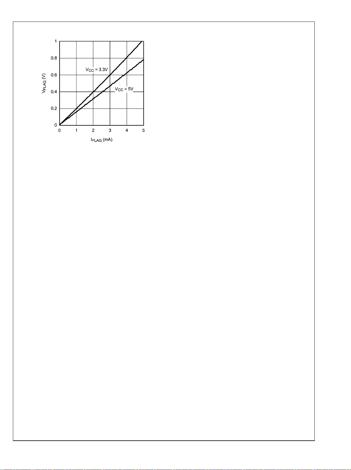
FLAG Voltage vs Current
LM3881
30048420
5 www.national.com
 Loading...