


查询LM3710XQBP-308供应商
LM3710/LM3711
Microprocessor Supervisory Circuits with Power Fail
Input, Low Line Output, Manual Reset and Watchdog
Timer
June 2002
LM3710/LM3711 Microprocessor Supervisory Circuits with Power Fail Input, Low Line Output,
Manual Reset and Watchdog Timer
General Description
The LM3710/LM3711 series of microprocessor supervisory
circuits provide the maximum flexibility for monitoring power
supplies and battery controlled functions in systems without
backup batteries. The LM3710/LM3711 series are available
in MSOP-10 and 9-bump micro SMD packages.
Built-in features include the following:
Reset: Reset is asserted during power-up, power-down, and
brownout conditions. RESET is guaranteed down to V
1.0V.
Manual Reset Input: An input that asserts reset when pulled
low.
Power-Fail Input: A 1.225V threshold detector for power fail
warning, or to monitor a power supply other than V
Low Line Output: This early power failure warning indicator
goes low when the supply voltage drops to a value which is
2% higher than the reset threshold voltage.
Watchdog Timer: The WDI (Watchdog Input) monitors one of
the µP’s output lines for activity. If no output transition occurs
during the watchdog timeout period, reset is activated.
CC
.
CC
Features
n Standard Reset Threshold voltage: 3.08V
n Custom Reset Threshold voltages: For other voltages
between 2.2V and 5.0V in 10mV increments, contact
National Semiconductor Corp.
n No external components required
n Manual-Reset input
n RESET (LM3710) or RESET (LM3711) outputs
of
n Precision supply voltage monitor
n Factory programmable Reset and Watchdog Timeout
Delays
n Separate Power Fail comparator
n Available in micro SMD package for minimum footprint
±
n
0.5% Reset threshold accuracy at room temperature
±
n
2% Reset threshold accuracy over temperature
extremes
n Reset assertion down to 1V V
n 28 µA VCCsupply current
(RESET option only)
CC
Applications
n Embedded Controllers and Processors
n Intelligent Instruments
n Automotive Systems
n Critical µP Power Monitoring
Typical Application
20011803
© 2002 National Semiconductor Corporation DS200118 www.national.com
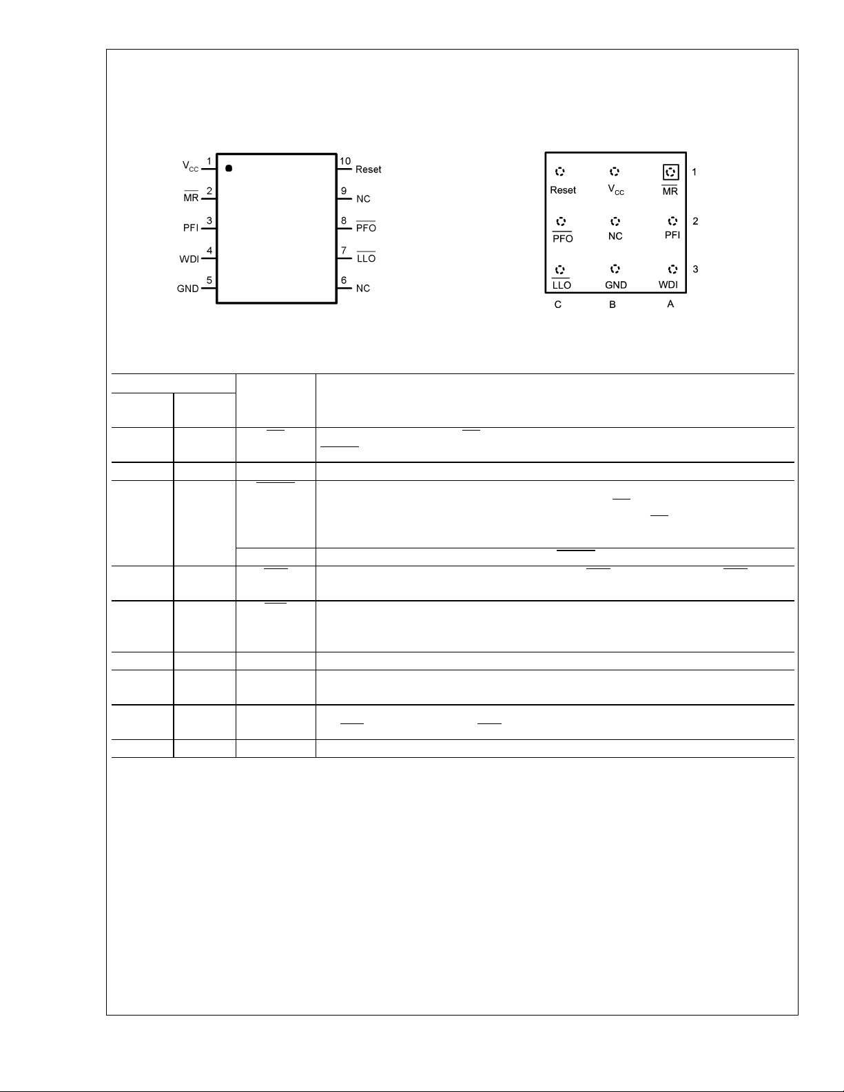
Connection Diagram
LM3710/LM3711
MSOP-10
Top View
(looking from the coating side)
micro SMD 9 Bump Package
BPA09
20011802
20011801
Pin Descriptions
Pin No.
micro
SMD
MSOP
A1 2 MR
B1 1 V
C1 10 RESET
C2 8 PFO Power-Fail Logic Output. When PFI is below V
C3 7 LLO
B3 5 GND Ground reference for all signals.
A3 4 WDI Watchdog Input Transition Monitor: If no transition activity occurs for a period exceeding
A2 3 PFI Power-Fail Comparator Input. When PFI is less than V
B2 6, 9 NC No Connect. Test input used at factory only. Leave floating.
Name Function
Manual-Reset input. When MR is less than V
(Manual Reset Threshold)
MRT
RESET/RESET is engaged.
CC
Power Supply input.
Reset Logic Output. Pulses low for tRP(Reset Timeout Period) when triggered, and stays
low whenever V
is below the reset threshold or when MR is below V
CC
for tRPafter either VCCrises above the reset threshold, or after MR input rises above
V
(LM3710 only).
MRT
RESET Reset Logic Output. RESET is the inverse of RESET (LM3711 only).
, PFO goes low; otherwise, PFO
PFT
remains high.
Low-Line Logic Output. Early Power-Fail warning output. Low when VCCfalls below V
(Low-Line Output Threshold). This output can be used to generate an NMI (Non-Maskable
Interrupt) to provide an early warning of imminent power-failure.
(Watchdog Timeout Period), reset is engaged.
t
WD
(Power-Fail Reset Threshold),
PFT
the PFO goes low; otherwise, PFO remains high.
. It remains low
MRT
LLOT
www.national.com 2
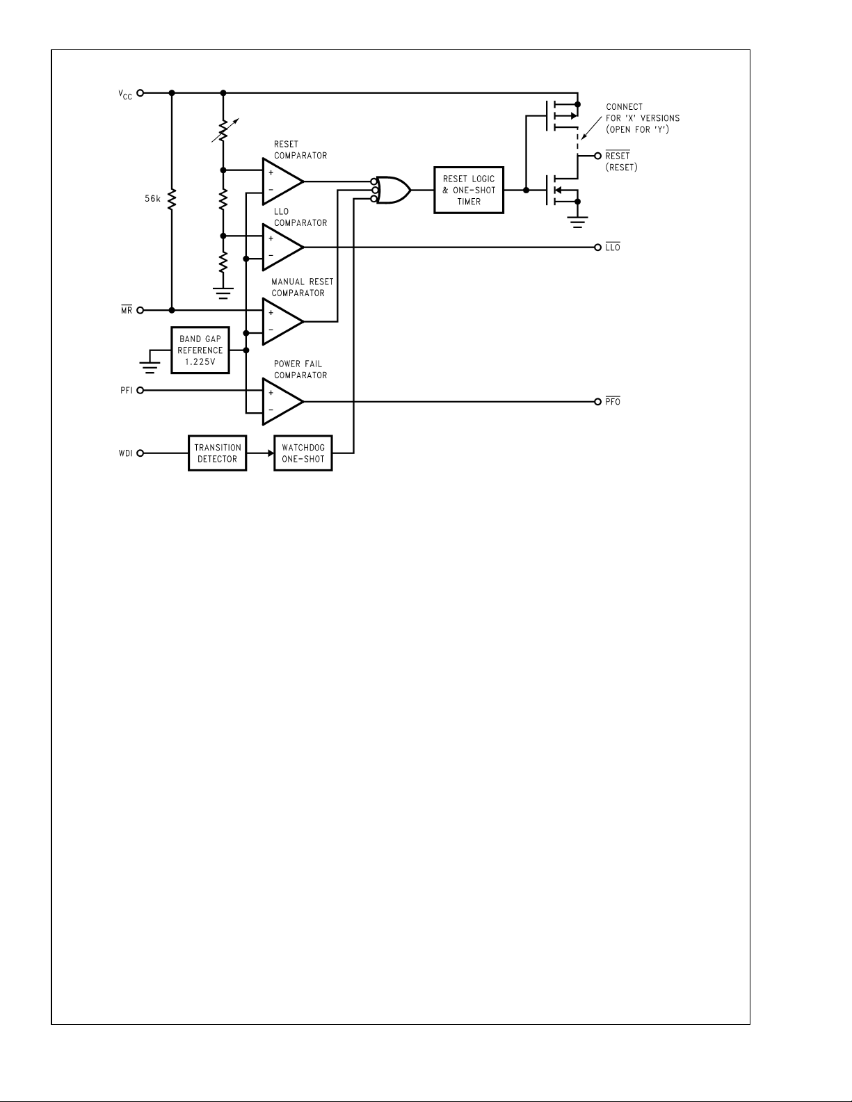
Block Diagram
LM3710/LM3711
20011805
www.national.com3
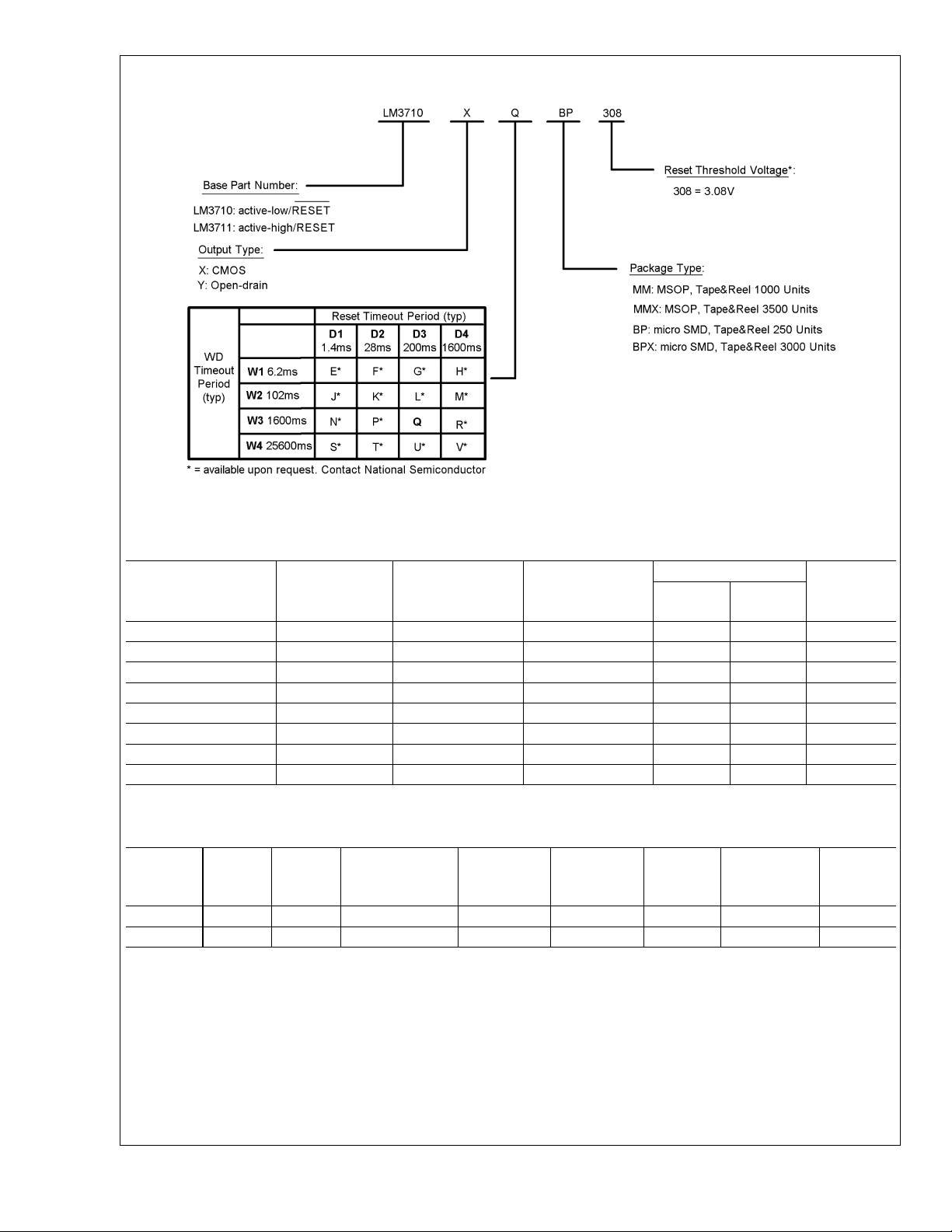
Ordering Information
LM3710/LM3711
*
For other voltages between 2.2V and 5.0V, please contact National Semiconductor sales office.
20011804
LM3710/LM3711
Part Number Output
Reset Timeout
Period
Watchdog
Timeout
Period
MSOP
Package
micro
SMD
Package
Marking
LM3710XQBP-308 totem-pole 200ms 1600ms x %%IA
LM3710XQBPX-308 totem-pole 200ms 1600ms x %%IA
LM3710XQMM-308 totem-pole 200ms 1600ms x R37B
LM3710XQMMX-308 totem-pole 200ms 1600ms x R37B
LM3711XQBP-308 totem-pole 200ms 1600ms x %%IB
LM3711XQBPX-308 totem-pole 200ms 1600ms x %%IB
LM3711XQMM-308 totem-pole 200ms 1600ms x R38B
LM3711XQMMX-308 totem-pole 200ms 1600ms x R38B
%% is the datecode and will vary with time.
Table Of Functions
Part
Number
LM3710 x X, Y
LM3711 x X Customized Customized x x x
*
= available upon request. Contact National
Active
Low
Reset
Active
High
Reset
Output
(X = totem-pole)
(Y = open-drain)
*
Reset
Timeout
Period
Watchdog
Timeout
Period
Manual
Reset
Power Fail
Comparator
Low
Line
Output
Customized Customized x x x
www.national.com 4
LM3710/LM3711
Absolute Maximum Ratings (Note 1)
Power Dissipation (Note 3)
If Military/Aerospace specified devices are required,
please contact the National Semiconductor Sales Office/
Distributors for availability and specifications.
Supply Voltage (V
All Other Inputs −0.3V to V
) −0.3V to 6.0V
CC
CC
+ 0.3V
Operating Ratings (Note 1)
Temperature Range −40˚C ≤ T
≤ 85˚C
J
ESD Ratings (Note 2)
Human Body Model
Machine Model
1.5kV
150V
LM3710/LM3711 Series Electrical Characteristics
Limits in the standard typeface are for TJ= 25˚C and limits in boldface type apply over full operating range. Unless otherwise
specified: V
Symbol Parameter Conditions Min Typ Max Units
POWER SUPPLY
V
CC
I
CC
RESET THRESHOLD
V
RST
V
RSTH
t
RP
t
RD
RESET (LM3711)
V
OL
V
OH
I
LKG
RESET (LM3710)
V
OL
V
OH
= +2.2V to 5.5V.
CC
Operating Voltage
Range: V
CC
VCCSupply
LM3710 1.0 5.5
LM3711 1.2 5.5
All inputs = VCC; all outputs floating 28 50 µA
Current
Reset Threshold VCCfalling −0.5
−2
falling: TA= 0˚C to 70˚C −1.5 +1.5
V
CC
Reset Threshold
Hysteresis
Reset Timeout
Period
VCCto Reset
Reset Timeout Period = E, J, N, S
Reset Timeout Period = F, K, P, T
Reset Timeout Period = G, L, Q, U
Reset Timeout Period = H, M, R, V
1
20
140
1120
VCCfalling at 1mV/µs 20 µs
Delay
V
V
V
V
V
V
>
2.25V, I
CC
>
2.7V, I
CC
>
4.5V, I
CC
>
1.2V, I
CC
>
1.8V, I
CC
>
2.25V, I
CC
>
2.7V, I
CC
>
4.5V, I
CC
= 5.5V 1.0 µA
RESET
= 900µA 0.3
SINK
= 1.2mA 0.3
SINK
= 3.2mA 0.4
SINK
SOURCE
SOURCE
SOURCE
SOURCE
= 50µA 0.8 V
= 150µA 0.8 V
SOURCE
= 300µA 0.8 V
= 500µA 0.8 V
= 800µA VCC− 1.5V
RESET V
RESET V
Output Leakage
Current
RESET V
RESET V
>
1.0V, I
CC
>
V
1.2V, I
CC
>
V
2.25V, I
CC
>
V
2.7V, I
CC
>
V
4.5V, I
CC
>
2.25V, I
CC
>
V
2.7V, I
CC
>
V
4.5V, I
CC
= 50µA 0.3
SINK
= 100µA 0.3
SINK
= 900µA 0.3
SINK
= 1.2mA 0.3
SINK
= 3.2mA 0.4
SINK
SOURCE
SOURCE
SOURCE
= 300µA 0.8 V
= 500µA 0.8 V
= 800µA VCC− 1.5V
+0.5
V
RST
0.0032•V
RST
1.4
28
200
1600
CC
CC
CC
CC
CC
CC
+2
mV
2
40
280
2240
V
%
ms
VV
V
V
www.national.com5
 Loading...