

July 7, 2008
LM3687
Step-Down DC-DC Converter with Integrated Low Dropout
Regulator and Startup Mode
LM3687 Step-Down DC-DC Converter with Integrated Low Dropout Regulator and Startup Mode
General Description
The LM3687 is a step-down DC-DC converter with an integrated low dropout Linear Regulator optimized for powering
ultra-low voltage circuits from a single Li-Ion cell or 3 cell
NiMH/NiCd batteries. It provides a dual output with fixed output voltages and combined load current up to 750mA in post
regulation mode or 1100mA in independent mode of operation, over an input voltage range from 2.7V to 5.5V. There are
several different fixed output voltage combinations available
(refer to table 'Voltage Options').
The Linear Regulator being driven from the fixed output voltage of the buck converter (post regulation) translates to high
efficiency.
The device offers superior features and performance for mobile phones and similar portable applications with complex
power management systems. Automatic intelligent switching
between PWM low-noise and PFM low-current mode offers
improved efficiency over the full load current range. During
full-power operation, a fixed-frequency 1.8MHz (typ.) PWM
mode drives loads from ~80mA to 750mA max. Hysteretic
PFM mode extends the battery life through reduction of the
quiescent current during light loads and system standby.
The LM3687 also features internal protection against overtemperature, current overload and under-voltage conditions.
Two enable pins allow the separate operation of either the
DC-DC or the Linear Regulator alone or both. If the power
input voltage for the Linear Regulator V
high (e.g. the DC-DC converter is not enabled or starting up)
a startup LDO supplies the Linear Regulator Output from
V
for 50mA rated load current (Startup Mode). If V
BATT
is at the required voltage level, the startup LDO is deactivated
and the main regulator provides 350mA output current. In
shutdown mode (Enable pins pulled low) the device turns off
and reduces battery consumption to 0.1µA (typ.).
The LM3687 is available in a tiny, lead-free (NO PB) 9-bump
micro SMD package. A high switching frequency of 1.8MHz
(typ.) allows the use of tiny surface-mount components. Only
four external components -one inductor and three ceramic
capacitors- are required.
is not sufficiently
IN_LIN
IN_LIN
Features
DC-DC Converter:
750mA maximum load capability
■
1.8MHz PWM fixed switching frequency (typ.)
■
Automatic PFM/PWM mode switching
■
27µA typ. Quiescent Current
■
Internal synchronous rectification for high efficiency
■
Internal soft start
■
Dual Rail Linear Regulator:
Startup Mode
■
Load transients < 25mVpeak typ.
■
Line transients < 1mVpeak typ.
■
Very Low Dropout Voltage: 82mV typ. at 350mA load
■
current
0.7V ≤ V
■
10µA typical IQ from V
■
350mA maximum load capability
■
Combined Common Features:
65µA typical Quiescent Current from V
■
regulators are enabled
750mA maximum combined load capability in post
■
regulation setup (DC-DC 400mA + Linear Regulator
350mA)
1100mA maximum total load capability in independent
■
mode of operation (DC-DC: 750mA, Linear Regulator:
350mA)
Operates from a single Li-Ion cell or 3 cell NiMH/NiCd
■
batteries
Only four tiny surface-mount external components
■
required (one inductor, three ceramic capacitors)
Small 9-bump micro SMD package
■
Over-temperature, current overload and under-voltage
■
protection
IN_LIN
≤ 4.5V
IN_LIN
BATT
if both
Applications
Mobile Phones
■
Hand-Held Radios
■
Personal Digital Assistants
■
Palm-top PCs
■
Portable Instruments
■
Battery Powered Devices
■
© 2008 National Semiconductor Corporation 202101 www.national.com

Typical Application Circuit
LM3687
FIGURE 1. Typical Application Circuit: Linear Regulator as Post Regulator
20210101
FIGURE 2. Typical Application Circuit: Independent Mode of Operation
www.national.com 2
20210105

Connection Diagrams
LM3687
Connection Diagram 9-Bump Thin Micro SMD Package
20210104
Top View
20210102
Package Mark
Large Bump, 0.5mm Pitch,
See NS Package TLA09
Note:The actual physical placement of the package marking will vary from part to part. The package marking "X" designates the
date code. "T" is a NSC internal code for die traceability. Both will vary considerably. "BC" identifies the device (part number, option,
etc.)
Pin Descriptions
Pin Number Pin Name Description
A1 PGND Power Ground pin
A2 SGND Signal Ground pin
A3 V
OUT_LIN
B1 SW Switching Node Connection to the internal PFET switch and NFET synchronous rectifier
B2 EN_DCDC Enable Input for the DC-DC converter. The DC-DC converter is in shutdown mode if voltage at this
B3 V
C1 V
IN_LIN
BATT
C2 FB_DCDC Feedback Analog Input for the DC-DC converter. Connect directly to the output filter capacitor.
C3 EN_LIN Enable Input for the linear regulator. The linear regulator is in shutdown mode if voltage at this pin
Voltage Output of the linear regulator
pin is < 0.4V and enabled if > 1.0V. Do not leave this pin floating. Please see section 'Enable
Combinations'.
Power Supply Input for the linear regulator
Power Supply for the DC-DC output stage and internal circuitry. Connect to the input filter capacitor
(see typical application).
is < 0.4V and enabled if > 1.0V. Do not leave this pin floating. Please see section 'Enable
Combinations'.
Voltage Options
DC-DC Converter Output:
V
OUT_DCDC
1.80V 1.50V
1.80V 1.20V
1.80V * 1.30V *
* For availability of these or other output voltage combinations please contact your local NSC sales office
Linear Regulator Output:
V
OUT_LIN
3 www.national.com

Enable Combinations
LM3687
EN_DCDC EN_LIN Comments
0 0 No Outputs
0 1 Linear Regulator enabled only *
1 0 DC-DC converter enabled only
1 1 DC-DC converter and linear regulator active *
* Startup Mode:
V
must be higher than V
IN_LIN
If V
IN_LIN
< V
OUT_LIN(NOM)
OUT_LIN(NOM)
+ 100mV (100mV hysteresis), the startup LDO (I
+ 200mV in order to enable the main regulator (I
= 50mA) is active, supplied from V
MAX
= 350mA).
MAX
BATT
For example in the typical post regulation application the LDO will remain in startup mode until the DC-DC converter has ramped
up its output voltage.
Order Information
.
Output Voltage Option
V
OUT_DCDC
V
OUT_LIN
1.80V 1.50V
1.80V 1.20V
1.80V * 1.30V *
Order Number Package Marking Supplied as Flow
LM3687TL-1815 S9
LM3687TLX-1815
S9 3000 units, tape and
LM3687TL-1812 SB
LM3687TLX-1812 SB
LM3687TL-1813 tbd
LM3687TLX-1813 tbd
250 units, tape and reel,
reel, lead free
250 units, tape and reel,
3000 units, tape and
reel, lead free
250 units, tape and reel,
3000 units, tape and
reel, lead free
* For availability or other output voltage combinations please contact your local NSC sales office
lead free
lead free
lead free
NOPB
NOPB
NOPB
NOPB
NOPB
NOPB
www.national.com 4
LM3687
Absolute Maximum Ratings (Notes 2, 1)
If Military/Aerospace specified devices are required,
please contact the National Semiconductor Sales Office/
Distributors for availability and specifications.
V
, V
IN_LIN
V
IN_LIN
V
IN_LIN
Enable pins,
Feedback pin,
SW pin
Continuous Power Dissipation
(Note 3) Internally Limited
Junction Temperature (T
Storage Temperature Range -65°C to + 150°C
Package Peak Reflow Temperature
(Pb-free, 10-20 sec.) (Note 4) 260°C
ESD Rating (Note 5)
Human Body Model: 2.0kV
Machine Model 200V
pins: Voltage to GND,
BATT
≤ V
BATT
pin to V
pin 0.2V
BATT
-0.2V to 6.0V
(GND-0.2V) to
(V
BATT
) 150°C
J-MAX
+0.2V) with
6.0V max
Operating Ratings
(Notes 1, 2)
Input Voltage Range V
(Note 12)
BATT
(≥V
2.7V to 5.5V
OUT_LIN(NOM)
+ 1.5V
and
≥V
OUT_DCDC(NOM)
1.0V)
Input Voltage Range V
IN_LIN
(V
OUT_LIN(NOM)
+ 0.25V)
to 4.5V
Junction Temperature (TJ) Range -30°C to + 125°C
Ambient Temperature (TA) Range
-30°C to + 125°C
(Note 6)
Thermal Properties
Junction-to-Ambient Thermal
Resistance (θJA), for 4 layer board
(Note 7)
Micro SMD 9 70°C/W
+
ESD Caution Notice
National Semiconductor recommends that all integrated circuits be handled with appropriate precautions. Failure to observe proper
ESD handling techniques can result in damage.
Electrical Characteristics (Notes 2, 8) Typical values and limits appearing in standard typeface are for T
25°C. Limits appearing in boldface type apply over the full operating temperature range: -30°C ≤ TJ ≤ +125°C. Unless otherwise
noted, V
10µF, C
= V
IN_LIN
VOUT_LIN
OUT_LIN(NOM)
= 2.2µF, C
+ 0.3V, V
= 1.0µF, L = 2.2µH.
VIN_LIN
BATT
= 3.6V, I
OUT_LIN
= 1mA, V
EN_DCDC
= V
EN_LIN
= V
BATT
, C
VBATT
= 4.7µF, C
VOUT_DCDC
=
A
=
DC-DC Converter (Note 11)
Symbol Parameter Conditions Typical Limit Units
Min Max
V
FB_DCDC
R
DSON(P)
R
DSON(N)
I
LIM_DCDC
F
OSC
Feedback Voltage
Accuracy
Line Regulation
Load Regulation
Pin-Pin Resistance for
PFET
Pin-Pin Resistance for
NFET
Switch Peak Current
Limit
Internal Oscillator
Frequency
PWM Mode -2.5 +2.5 %
V
OUT_DCDC
+ 1.0V ≤ V
BATT
≤ 5.5V, I
OUT_DCDC
0.06 %/V
= 150mA
100mA ≤ I
OUT_DCDC
≤ 750mA
0.0005 %/mA
280 500
200 400
Open loop (Note 14) 1172 994 1380 mA
PWM Mode 1.8 1.3 2.3 MHz
mΩ
mΩ
5 www.national.com

Linear Regulator, Normal Mode
LM3687
ΔV
V
OUT_LIN(NOM)
ΔV
ΔV
ΔV
ΔV
ΔV
V
DO_VIN_LIN
I
Q_VIN_LIN
I
SC_LIN
PSRR
E
N
ΔV
ΔV
Symbol Parameter Condition Typ Limit Units
Min Max
OUT_LIN
OUT_LIN
IN_LIN
OUT_LIN
BATT
OUT_LIN
/
/
/
/ ΔmA
Output Voltage
Accuracy
Line Regulation Error
Load Regulation Error
Output Voltage
Dropout
(Note 10)
Quiescent Current into
V
IN_LIN
Shutdown Current into
V
IN_LIN
Output Current
In startup and normal mode
V
IN_LIN
4.5V, V
V
BATT
= V
OUT_LIN(NOM)
= 4.5V
BATT
= V
OUT_LIN(NOM)
+ 0.3V to
+ 1.5V
-1.5
-2.0
0.3 1 mV/V
0.5 3.1
1.5
2.0
(≥2.7V) to 5.5V
I
= 1mA to 350mA 10 60 µV/mA
OUT_LIN
I
= 350mA ,
OUT_LIN
V
BATT
= V
OUT_LIN(NOM)
+ 1.5V
(≥2.7V) 85
I
= 150mA ,
OUT_LIN
V
BATT
= V
OUT_LIN(NOM)
+ 1.3V
(≥2.7V) 42
I
= 0mA 10 28 µA
OUT_LIN
V
= 0V 0.1 1 µA
EN_LIN
V
= 0V 500 350 mA
OUT_LIN
200 mV
100 mV
(short circuit)
Power Supply
Rejection Ratio
Output Noise linear
Sine modulated V
f = 10Hz
f = 100Hz
f = 1kHz
Sine modulated V
f = 10Hz
f = 100Hz
f = 1kHz
f = 10kHz
10Hz - 100kHz 100 µV
BATT
IN
,
70
65
45
80
90
95
85
regulator
V
OUT_LIN
OUT_LIN
Dynamic line transient
response V
IN_LIN
Dynamic line transient
response V
BATT
Dynamic load transient
response
= V
IN_LIN
V
OUT_LIN(NOM)
OUT_LIN(NOM)
+ 0.9V
tr, tf = 10µs
V
= V
BATT
V
OUT_LIN(NOM)
OUT_LIN(NOM)
+ 2.1V
tr, tf = 10µs
Pulsed load 0 ... 350mA
di/dt = 350mA/1µs
+ 0.3V to
+ 1.5V to
±1 mVp
±15 mVp
±30 mVp
%
%
dB
dB
RMS
Startup LDO
Symbol Parameter Conditions Typical Limit Units
Min Max
I
OUT
I
SC_LIN
www.national.com 6
Rated output current 50 mA
Output Current (short
V
OUT_LIN
= 0V 100 50 mA
circuit)

System Parameters Supply
LM3687
Symbol Parameter Conditions Typical
I
Q_VBATT
Quiescent current
into V
BATT
EN_LIN = low, EN_DCDC = high, I
I
= 0mA, DC-DC is not switching
OUT_LIN
(FB_DCDC forced higher than V
OUT_DCDC
OUT_DCDC
)
=
27
Limit
Min Max
60 µA
EN_LIN = high, EN_DCDC = low 55 µA
EN_LIN = EN_DCDC = high 65 µA
Shutdown current into
V
BATT
V
EN_DCDC
= V
EN_LIN
-30°C ≤ TJ ≤ +85°C
= 0V
0.1
5 µA
Under-Voltage Protection
Symbol Parameter Conditions Typical Limit Units
Min Max
V
BATT_UVP
V
BATT_EN
Under-Voltage
Lockout
System Enable
Voltage
2.41 V
2.65 V
Enable Pins (EN_DCDC, EN_LIN)
Symbol Parameter Conditions Typical
I
EN
V
IH
V
IL
Enable pin input
current
Logic High voltage
level
Logic Low voltage
level
0.01 1 µA
1.0 V
0.4 V
Limit
Min Max
Units
Units
Thermal Protection
Symbol Parameter Conditions Typical
T
SHDN
(Note 15)
ΔT
SHDN
Thermal-Shutdown
Temperature
Thermal-Shutdown
Hysteresis
160 °C
20 °C
Limit
Min Max
Units
7 www.national.com
External Components, Recommended Specification (Note 13)
LM3687
Symbol Parameter Conditions Value
C
VOUT_LIN
C
VIN_LIN
C
VBATT
C
VOUT_DCDC
C
ESR
L
Note 1: Absolute Maximum Ratings indicate limits beyond which damage to the component may occur. Operating Ratings are conditions under which operation
of the device is guaranteed. Operating Ratings do not imply guaranteed performance limits. For guaranteed performance limits and associated test conditions,
see the Electrical Characteristics tables.
Note 2: All voltages are with respect to the potential at the SGND pin.
Note 3: Internal thermal shutdown circuitry protects the device from permanent damage. Thermal shutdown engages at TJ = 160°C (typ.) and disengages at T
= 140°C (typ.).
Note 4: For detailed soldering specifications and information, please refer to National Semiconductor Application Note 1112: Micro SMD Wafer Level Chip Scale
Package (AN-1112).
Note 5: The Human body model is a 100pF capacitor discharged through a 1.5kΩ resistor into each pin. The machine model is a 200pF capacitor discharged
directly into each pin. (MIL-STD-883 3015.7)
Note 6: In applications where high power dissipation and/or poor package thermal resistance is present, the maximum ambient temperature may have to be
derated. Maximum ambient temperature (T
dissipation of the device in the application (P
following equation: T
Note 7: Junction-to-ambient thermal resistance is highly application and board-layout dependent. In applications where high maximum power dissipation exists,
special attention must be paid to thermal dissipation issues in board design.
Note 8: Min and Max limits are guaranteed by design, test, or statistical analysis. Typical numbers are not guaranteed, but do represent the most likely norm.
Unless otherwise specified, conditions for typ. specifications are: V
Note 9: Dropout voltage is defined as the input to output voltage differential at which the output voltage falls to 100mV below the nominal output voltage.
Note 10: This specification does not apply if the battery voltage V
Note 11: The parameters in the electrical characteristic table are tested at V
refer to datasheet curves.
Note 12: The battery input voltage range recommended for ideal applications performance for the specified output voltages is given as follows: V
5.5V for 1.0V < V
Note 13: The capacitor tolerance should be 30% or better over temperature. The full operating conditions for the application should be considered when selecting
a suitable capacitor to ensure that the minimum value of capacitance is always met. Recommended capacitor type is X7R. However, dependent on application,
X5R, Y5V, and Z5U can also be used. The shown minimum limit represents real minimum capacitance, including all tolerances and must be maintained over
temperature and dc bias voltage (See capacitor section in Applications Hints)
Note 14: Refer to datasheet curves for closed loop data and its variation with regards to supply voltage and temperature. Electrical Characteristic table reflects
open loop data (FB=0V and current drawn from SW pin ramped up until cycle by cycle current limit is activated). Closed loop current limit is the peak inductor
current measured in the application circuit by increasing output current until output voltage drops by 10%.
Note 15: The DC-DC converter will only enter thermal shutdown from PWM mode. At light loads -present for PFM mode- no significant contribution to the power
dissipation is added by the DC-DC converter.
Output Capacitance for
linear regulator
Input Capacitance for
linear regulator
Input Capacitance for
DC-DC converter
DC-DC converter output
filter capacitor
V
is biased separately, not by
IN_LIN
V
OUT_DCDC
(no C
VIN_LIN
needed for
2.2 1.5 10 µF
post regulation application) 1.0 0.47 µF
4.7 µF
10 µF
ESR of all capacitors 0.003 0.300
Inductance 2.2 µH
I
SAT
1.6 A
DCR 200
) is dependent on the maximum operating junction temperature (T
A-MAX
OUT_DCDC
= T
J-MAX-OP
< 1.8V; V
A-MAX
D-MAX
– (θJA × P
= (V
BATT
), and the junction-to ambient thermal resistance of the part/package in the application (θJA), as given by the
).
D-MAX
= 3.6V and TA = 25°C.
BATT
needs to be decreased below the minimum operating limit of 2.7V.
+1V) to 5.5V for 1.8V ≤ V
OUT_DCDC
BATT
= 3.6V unless otherwise specified. For performance over the input voltage range
BATT
≤ 1.875V
OUT_DCDC
J-MAX-OP
Limit
Min Max
= 125°C), the maximum power
BATT
Units
Ω
mΩ
J
= 2.7V to
www.national.com 8

Block Diagram
LM3687
Simplified Block Diagram
20210106
9 www.national.com

Typical Performance Characteristics Unless otherwise specified, typical application (post regulation),
V
BATT
LM3687
= 3.6V, TA = 25°C, enable pins tied to V
I
Q_VBATT
vs. V
, LDO disabled
BATT
BATT
, V
OUT_DCDC
= 1.8V, V
OUT_LIN
= 1.2V
I
Q_VBATT
vs. V
, both enabled
BATT
V
OUT_DCDC
V
OUT_DCDC
vs. I
OUT_DCDC
vs. Temperature
20210109
20210111
V
V
OUT_LIN
vs. I
OUT_LIN
OUT_LIN
vs. Temperature
20210110
20210112
20210113
www.national.com 10
20210114

LM3687
Efficiency DC-DC vs. Output Current
LDO disabled
Startup into load
20210134
Startup into no load
V
Line Transient Response (PWM Mode)
BATT
20210115
V
Line Transient Response
IN_LIN
20210116
20210118
20210117
Load Transient Response DC-DC
(PWM Mode: 100mA to 750mA)
20210119
11 www.national.com

LM3687
Load Transient Response DC-DC
(PFM Mode: 1mA to 50mA)
Load Transient Response Linear Regulator
0mA to 350mA
Mode Change by Load Transients
(PFM to PWM)
Output Ripple PFM Mode
20210120
20210122
20210121
Mode Change by Load Transients
(PWM to PFM)
20210123
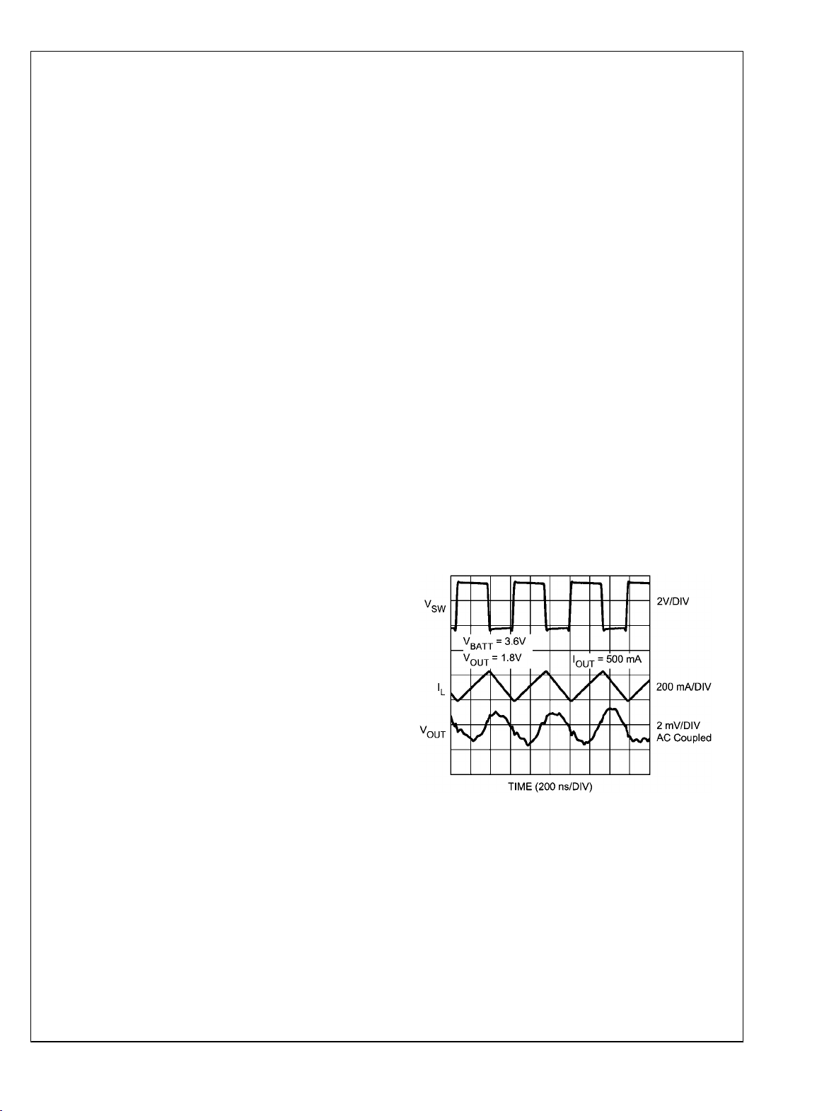
Output Ripple PWM Mode
20210135
www.national.com 12
20210136
LM3687
Operation Description
DEVICE INFORMATION
The LM3687 incorporates a high efficiency synchronous
switching step-down DC-DC converter and a very low dropout
linear regulator.
The DC-DC converter delivers a constant voltage from a single Li- Ion battery and input voltage rails from 2.7V to 5.5V to
portable devices such as cell phones and PDAs. Using a voltage mode architecture with synchronous rectification, it has
the ability to deliver up to 750mA load current depending on
the input voltage, output voltage, ambient temperature and
the inductor chosen.
The linear regulator delivers a constant voltage biased from
V
power input - typically the output voltage of the DC-DC
IN_LIN
converter is used (post regulation) - with a maximum load
current of 350mA.
Two enable pins allow the independent control of the two outputs. Shutdown mode turns off the device, offering the lowest
current consumption (I
SHUTDOWN
Besides the shutdown feature, for the DC-DC converter there
are two more modes of operation depending on the current
required:
- PWM (Pulse Width Modulation), and
- PFM (Pulse Frequency Modulation).
The device operates in PWM mode at load current of approx-
imately 80 mA or higher. Lighter load currents cause the
device to automatically switch into PFM for reduced current
consumption (I
= 27 µA typ) and a longer battery life.
Q_VBATT
Additional features include soft-start, startup mode of the linear regulator, under-voltage protection, current overload protection, and over-temperature protection.
As shown in Figure 1: 'Typical Application Circuit: Linear Regulator as Post Regulator', only four external surface-mount
components are required for implementation -one inductor
and three ceramic capacitors.
An internal reference generates 1.8V biasing an internal resistive divider to create a reference voltage range from 0.45V
to 1.8V (in 50mV steps) for the linear regulator (depending on
the output voltage setting defined in the fab) and the 0.5V
reference used for the DC-DC converter.
The Under-voltage lockout feature enables the device to startup once V
device off if V
has reached 2.65V typically and turns the
BATT
drops below 2.41V typically.
BATT
Note:
In the case that the DC-DC converter is switched off while the
Linear Regulator is still enabled, an overshoot of up to 150mV
might appear at V
present:
-high V
BATT
-down ramp on V
Linear Regulator into dropout
OUT_LIN
of greater than 100mV/16us taking the
IN_LIN
-light load on Linear Regulator
DC-DC CONVERTER OPERATION
During the first part of each switching cycle, the control block
in the LM3687 turns on the internal PFET switch. This allows
current to flow from the input V
and the inductor to the output filter capacitor and load. The
inductor limits the current to a ramp with a slope of (V
V
OUT_DCDC
) / L, by storing energy in the magnetic field.
During the second part of each cycle, the controller turns the
PFET switch off, blocking current flow from the input, and then
= 0.1 µA typ).
, if all of the following conditions are
through the switch pin SW
BATT
BATT
turns the NFET synchronous rectifier on. The inductor draws
current from ground through the NFET to the output filter capacitor and load, which ramps the inductor current down with
a slope of (- V
OUT_DCDC
/ L).
The output filter stores charge when the inductor current is
high, and releases it when low, smoothing the voltage across
the load.
The output voltage is regulated by modulating the PFET
switch on time to control the average current sent to the load.
The effect is identical to sending a duty-cycle modulated rectangular wave formed by the switch and synchronous rectifier
at the SW pin to a low-pass filter formed by the inductor and
output filter capacitor. The output voltage is equal to the average voltage at the SW pin.
PWM Operation
During PWM (Pulse Width Modulation) operation the converter operates as a voltage-mode controller with input voltage feed forward. This allows the converter to achieve good
load and line regulation. The DC gain of the power stage is
proportional to the input voltage. To eliminate this dependency, feed forward inversely proportional to the input voltage is
introduced.
While in PWM mode, the output voltage is regulated by
switching at a constant frequency and then modulating the
energy per cycle to control power to the load. At the beginning
of each clock cycle the PFET switch is turned on and the inductor current ramps up until the duty-cycle-comparator trips
and the control logic turns off the switch. The current limit
comparator can also turn off the switch in case the current
limit of the PFET is exceeded. Then the NFET switch is turned
on and the inductor current ramps down. The next cycle is
initiated by the clock turning off the NFET and turning on the
PFET.
20210124
FIGURE 3. Typical PWM Operation
Internal Synchronous Rectification
While in PWM mode, the DC-DC converter uses an internal
NFET as a synchronous rectifier to reduce rectifier forward
voltage drop and associated power loss. Synchronous rectification provides a significant improvement in efficiency
whenever the output voltage is relatively low compared to the
voltage drop across an ordinary rectifier diode.
-
Current Limiting
A current limit feature allows the LM3687 to protect itself and
external components during overload conditions. PWM mode
implements current limiting using an internal comparator that
13 www.national.com

trips at 1172 mA (typ). If the output is shorted to ground the
device enters a timed current limit mode where the NFET is
turned on for a longer duration until the inductor current falls
LM3687
below a low threshold. This allows the inductor current more
time to decay, thereby preventing runaway.
PFM Operation
At very light load, the DC-DC converter enters PFM mode and
operates with reduced switching frequency and supply current to maintain high efficiency. The part automatically transitions into PFM mode when either of two conditions occurs
for a duration of 32 or more clock cycles:
A. The NFET current reaches zero.
B. The peak PMOS switch current drops below the I
el, (typically I
< 36mA + V
MODE
BATT
/ 35Ω ).
20210125
FIGURE 4. Typical PFM Operation
MODE
lev-
during PWM operation, allowing additional headroom for voltage drop during a load transient from light to heavy load. The
PFM comparators sense the output voltage via the feedback
pin and control the switching of the output FETs such that the
output voltage ramps between ~0.6% and ~1.7% above the
nominal PWM output voltage. If the output voltage is below
the ‘high’ PFM comparator threshold, the PMOS power switch
is turned on. It remains on until the output voltage reaches the
‘high’ PFM threshold or the peak current exceeds the I
level set for PFM mode. The typical peak current in PFM mode
is: I
= 134mA + V
PFM
BATT
/ 23Ω.
PFM
Once the PMOS power switch is turned off, the NMOS power
switch is turned on until the inductor current ramps to zero.
When the NMOS zero-current condition is detected, the
NMOS power switch is turned off. If the output voltage is below the ‘high’ PFM comparator threshold (see Figure 5), the
PMOS switch is again turned on and the cycle is repeated
until the output reaches the desired level. Once the output
reaches the ‘high’ PFM threshold, the NMOS switch is turned
on briefly to ramp the inductor current to zero and then both
output switches are turned off and the part enters an extremely low power mode. Quiescent supply current during this
‘sleep’ mode is 27µA (typ), which allows the part to achieve
high efficiency under extremely light load conditions.
If the load current should increase during PFM mode (see
Figure 5) causing the output voltage to fall below the ‘low2’
PFM threshold, the part will automatically transition into fixedfrequency PWM mode.
When V
mode at ~30mA output current and from PFM to PWM mode
at ~80mA , when V
pens at ~60mA and PFM to PWM transition happens at
~90mA, when V
at ~100mA and PFM to PWM transition happens at ~125mA.
=2.7V the part transitions from PWM to PFM
BATT
=3.6V, PWM to PFM transition hap-
BATT
=5.5V, PWM to PFM transition happens
BATT
During PFM operation, the DC-DC converter positions the
output voltage slightly higher than the nominal output voltage
20210126
FIGURE 5. Operation in PFM Mode and Transfer to PWM Mode
www.national.com 14

LM3687
Soft Start
The DC-DC converter has a soft-start circuit that limits in-rush
current during start-up. During start-up the switch current limit
is increased in steps. Soft start is activated only if EN_DCDC
goes from logic low to logic high after V
Soft start is implemented by increasing switch current limit in
reaches 2.7V.
BATT
steps of 85mA, 170mA, 340mA and 1120mA (typical switch
current limit). The start-up time thereby depends on the output
capacitor and load current demanded at start-up. Typical
start-up times with a 10µF output capacitor and 750mA load
is 455 µs and with 1mA load is 180µs.
LINEAR REGULATOR OPERATION
In the typical post regulation application the power input voltage V
converter. Using a buck converter to reduce the battery volt-
for the linear regulator is generated by the DC-DC
IN_LIN
age to a lower input voltage for the linear regulator translates
to higher efficiency and lower power dissipation.
It's also possible to operate the linear regulator independent
of the DC-DC converter output voltage either from V
different source. In this case it's important that V
not exceed V
regulator as well, it supplies internal circuitry.
An input capacitor of 1µF at V
other filter or bypass capacitor is present in the V
at any time. V
BATT
is needed for the linear
BATT
needs to be added if no
IN_LIN
BATT
IN_LIN
IN_LIN
or a
does
path.
Startup Mode
If the linear regulator is enabled (logic high at EN_LIN), the
power input voltage V
nominal output voltage of the linear regulator V
If V
offering a rated output current of 350mA and supplied by
V
If V
providing a reduced rated output current of 50mA typical,
supplied by V
100mV is established. This feature is intended to enable the
IN_LIN
IN_LIN
IN_LIN
> V
.
< V
OUT_LIN(NOM)
OUT_LIN(NOM)
. Between these two levels a hystersis of
BATT
is continuously compared to the
IN_LIN
OUT_LIN
.
+ 200mV the main regulator is active,
+ 100mV the startup LDO is active,
supply of loads at the output of the linear regulator while the
output of the DC-DC converter is still ramping up.
In the typical post regulation application with both enable pins
connected to V
BATT
and V
supplied by V
IN_LIN
OUT_DCDC
as an
example, the linear regulator turns on in startup mode (I
50mA) supplied out of V
converter turns on, but V
internal signal 'Mode Switch' monitors the voltage level of
V
. Once V
IN_LIN
ulator changes to normal mode (I
of V
linear regulator switches back to startup mode.
IN_LIN
. If V
> V
IN_LIN
drops below V
IN_LIN
FIGURE 6. Startup Sequence, V
. At the same time the DC-DC
BATT
OUT_DCDC
OUT_LIN(NOM)
startup time is longer. The
+ 200mV, the linear reg-
= 350mA) supplied out
MAX
OUT_LIN(NOM)
EN_DCDC
+ 100mV the
= V
EN_LIN
20210132
= V
MAX
BATT
Current Limiting
The LM3687 incorporates also a current limit feature for the
linear regulator to protect itself and external components during overload conditions at V
over-current condition at V
the NFET pass device will be limited.
OUT_LIN
. In the event of a peak
OUT_LIN
the output current through
=
15 www.national.com

Application Hints
LM3687
INDUCTOR SELECTION
There are two main considerations when choosing an inductor; the inductor should not saturate, and the inductor current
ripple should be small enough to achieve the desired output
voltage ripple. Different saturation current rating specifications are followed by different manufacturers so attention
must be given to details. Saturation current ratings are typically specified at 25°C. However, ratings at the maximum
ambient temperature of application should be requested from
the manufacturer. The minimum value of inductance to
guarantee good performance is 1.76µH at I
current over the ambient temperature range. Shielded in-
ductors radiate less noise and should be preferred. There are
two methods to choose the inductor saturation current rating.
Method 1
The saturation current should be greater than the sum of the
maximum load current and the worst case average to peak
inductor current. This can be written as:
I
> I
SAT
where
OUT_DCDC_MAX
+ I
RIPPLE
(typ) dc
LIM
•
I
: average to peak inductor current
RIPPLE
•
I
OUT_DCDCMAX
•
V
BATT
•
L: minimum inductor value including worst case tolerances
: maximum load current (750mA)
: maximum input voltage in application
(30% drop can be considered for method 1)
•
f: minimum switching frequency (1.3MHz)
Method 2
A more conservative and recommended approach is to
choose an inductor that has a saturation current rating greater
than the maximum current limit of 1380mA.
A 2.2 µH inductor with a saturation current rating of at least
1380mA is recommended for most applications. The
inductor’s resistance should be less than 0.3Ω for good efficiency. Table 1 lists suggested inductors and suppliers. For
low-cost applications, an unshielded bobbin inductor could be
considered. For noise critical applications, a toroidal or shielded- bobbin inductor should be used. A good practice is to lay
out the board with overlapping footprints of both types for design flexibility. This allows substitution of a low-noise shielded
inductor, in the event that noise from low-cost bobbin models
is unacceptable.
TABLE 1. Suggested Inductors and their Suppliers
Model Vendor Dimensions LxWxH (mm) DCR (max)
NR3015T2R2M Taiyo Yuden 3.0 x 3.0 x 1.5
LPS3015-222ML Coilcraft 3.0 x 3.0 x 1.5
DO3314-222MX Coilcraft 3.3 x 3.3 x 1.4
EXTERNAL CAPACITORS
As is common with most regulators, the LM3687 requires external capacitors to ensure stable operation. The LM3687 is
specifically designed for portable applications requiring minimum board space and the smallest size components. These
capacitors must be correctly selected for good performance.
INPUT CAPACITOR SELECTION
V
BATT
A ceramic input capacitor of 4.7 µF, 6.3V is sufficient for most
applications. Place the input capacitor as close as possible to
the V
improved input voltage filtering. Use X7R or X5R types; do
pin of the device. A larger value may be used for
BATT
not use Y5V. DC bias characteristics of ceramic capacitors
must be considered when selecting case sizes like 0805 and
0603. The minimum input capacitance to guarantee good
performance is 2.2µF at 3V dc bias; 1.5µF at 5V dc bias including tolerances and over ambient temperature range. The
input filter capacitor supplies current to the PFET switch of the
LM3687 DC-DC converter in the first half of each cycle and
reduces voltage ripple imposed on the input power source. A
ceramic capacitor’s low ESR provides the best noise filtering
of the input voltage spikes due to this rapidly changing current. Select a capacitor with sufficient ripple current rating.
The input current ripple can be calculated as:
V
IN_LIN
If the linear regulator is used as post regulation no additional
capacitor is needed at V
the DC-DC converter is close by and therefore sufficient.
In case of independent use, a 1.0µF ceramic capacitor is recommended at V
the V
IN_LIN
tance of not more than 1 cm from the V
returned to a clean analogue ground. Any good quality ceramic, tantalum, or film capacitor may be used at this input.
Important
Tantalum capacitors can suffer catastrophic failures due to
surge current when connected to a low-impedance source of
power (like a battery or a very large capacitor). If a tantalum
capacitor is used at this input, it must be guaranteed by the
72mΩ
110mΩ
200mΩ
as the output filter capacitor of
IN_LIN
if no other filter capacitor is present in
IN_LIN
supply path. This capacitor must be located a dis-
input pin and
IN_LIN
www.national.com 16

LM3687
manufacturer to have a surge current rating sufficient for the
application.
The ESR (Equivalent Series Resistance) of this input capacitor should be in the range of 3mΩ to 300mΩ. The tolerance
and temperature coefficient must be considered when selecting the capacitor to ensure the capacitance will remain ≥
470nF over the entire operating temperature range.
OUTPUT CAPACITOR
V
OUT_DCDC
A ceramic output capacitor of 10 µF, 6.3V is sufficient for most
applications. Use X7R or X5R types; do not use Y5V. DC bias
characteristics of ceramic capacitors must be considered
when selecting case sizes like 0805 and 0603. DC bias characteristics vary from manufacturer to manufacturer and dc
bias curves should be requested from them as part of the capacitor selection process.
The minimum output capacitance to guarantee good performance is 5.75µF at 1.8V DC bias including tolerances
and over ambient temperature range. The output filter ca-
pacitor smoothes out current flow from the inductor to the
load, helps maintain a steady output voltage during transient
load changes and reduces output voltage ripple. These capacitors must be selected with sufficient capacitance and
sufficiently low ESR to perform these functions.
The output voltage ripple is caused by the charging and discharging of the output capacitor and by the R
calculated as:
and can be
ESR
Voltage peak-to-peak ripple due to capacitance can be expressed as follow:
CAPACITOR CHARACTERISTICS
The LM3687 is designed to work with ceramic capacitors on
the outputs to take advantage of the benefits they offer. For
capacitance values in the range of 1µF to 4.7µF, ceramic capacitors are the smallest, least expensive and have the lowest
ESR values, thus making them best for eliminating high frequency noise. The ESR of a typical 1µF ceramic capacitor is
in the range of 3mΩ to 40mΩ, which easily meets the ESR
requirement for stability for the LM3687.
For both input and output capacitors, careful interpretation of
the capacitor specification is required to ensure correct device
operation. The capacitor value can change greatly, depending on the operating conditions and capacitor type.
In particular, the output capacitor selection should take account of all the capacitor parameters, to ensure that the
specification is met within the application. The capacitance
can vary with DC bias conditions as well as temperature and
frequency of operation. Capacitor values will also show some
decrease over time due to aging. The capacitor parameters
are also dependant on the particular case size, with smaller
sizes giving poorer performance figures in general. As an example, the graph below shows a comparison of different
capacitor case sizes in a Capacitance vs. DC Bias plot. As
shown in the graph, increasing the DC Bias condition can result in the capacitance value falling below the minimum recommended value. It is therefore recommended that the
capacitor manufacturers’ specifications for the nominal value
capacitor are consulted for all conditions, as some capacitor
sizes (e.g. 0402) may not be suitable in the actual application.
Voltage peak-to-peak ripple due to ESR can be expressed as
follow:
V
PP-ESR
= (2*I
RIPPLE
) * R
ESR
Because these two components are out of phase, the rms
(root mean squared) value can be used to get an approximate
value of peak-to-peak ripple. The peak-to-peak ripple voltage,
rms value can be expressed as follow:
Note that the output voltage ripple is dependent on the inductor current ripple and the equivalent series resistance of the
output capacitor (R
well as temperature dependent); make sure the value used
ESR
). The R
is frequency dependent (as
ESR
for calculations is at the switching frequency of the part.
V
OUT_LIN
The linear regulator is designed specifically to work with very
small ceramic output capacitors. A ceramic capacitor (dielectric types X7R, Z5U, or Y5V) in the 2.2µF range (up to 10µF)
and with an ESR between 3mΩ to 300mΩ is suitable as
C
in the LM3687 application circuit.
OUT_LIN
This capacitor must be located a distance of not more than
1cm from the V
ground. It is also possible to use tantalum or film capacitors
at the device output, V
for reasons of size and cost (see the section Capacitor Char-
pin and returned to a clean analogue
OUT_LIN
, but these are not as attractive
OUT_LIN
acteristics).
20210108
FIGURE 7. Graph Showing a Typical Variation In
Capacitance vs. DC Bias
The ceramic capacitor’s capacitance can vary with temperature. The capacitor type X7R, which operates over a temperature range of -55°C to +125°C, will only vary the capacitance
to within ±15%. The capacitor type X5R has a similar tolerance over a reduced temperature range of -55°C to +85°C.
Many large value ceramic capacitors, larger than 1µF are
manufactured with Z5U or Y5V temperature characteristics.
Their capacitance can drop by more than 50% as the temperature varies from 25°C to 85°C. Therefore X7R is recommended over Z5U and Y5V in applications where the ambient
temperature will change significantly above or below 25°C.
Tantalum capacitors are less desirable than ceramic for use
as output capacitors because they are more expensive when
17 www.national.com

comparing equivalent capacitance and voltage ratings in the
1µF to 4.7µF range.
LM3687
Another important consideration is that tantalum capacitors
have higher ESR values than equivalent size ceramics. This
means that while it may be possible to find a tantalum capacitor with an ESR value within the stable range, it would have
to be larger in capacitance (which means bigger and more
costly) than a ceramic capacitor with the same ESR value. It
should also be noted that the ESR of a typical tantalum will
increase about 2:1 as the temperature goes from 25°C down
to -40°C, so some guard band must be allowed. For the output
capacitor of the DC-DC converter, please note that the output
voltage ripple is dependent on the ESR of the output capacitor.
TABLE 2. Suggested Capacitors and their Suppliers
Capacitance / µF Model Voltage Rating Vendor Type Case Size / Inch (mm)
10.0 C1608X5R0J106K 6.3V TDK Ceramic, X5R 0603 (1608)
4.7 C1608X5R1A475K 10V TDK Ceramic, X5R 0603 (1608)
2.2 C1608X5R1A225K 10V TDK Ceramic, X5R 0603 (1608)
1.0 C1005X5R1A105K 10V TDK Ceramic, X5R 0402 (1005)
POWER DISSIPATION AND DEVICE OPERATION
The permissible power dissipation for any package is a measure of the capability of the device to pass heat from the power
source, the junctions of the IC, to the ultimate heat sink, the
ambient environment. Thus the power dissipation is dependent on the ambient temperature and the thermal resistance
across the various interfaces between the die and ambient
air.
As stated in (Note 6) in the electrical specification section, the
allowable power dissipation for the device in a given package
can be calculated using the equation:
P
D_SYS
= (T
J(MAX)
- TA) / θ
JA
For the LM3687 there are two different main sources contributing to the systems power dissipation (P
DC converter (P
Neglecting switching losses and quiescent currents these two
) and the linear regulator (P
D_DCDC
D_SYS
): the DC-
D_LIN
main contributors can be estimated by the following equations:
• P
= (V
D_LIN
• P
D_DCDC
with duty cycle D = V
IN_LIN
= I
OUT_DCDC
- V
OUT_LIN
2
* [(R
OUT_DCDC
) * I
OUT_LIN
DSON(P)
/ V
* D) + (R
.
BATT
DSON(N)
* (1-D))]
As an example, assuming the typical post regulation application, the conversion from V
and further to V
sults in following power dissipations:
P
3.6V)) = 177mW and
P
P
= (0.75A)2 * (0.38Ω * 1.8V / 3.6V + 0.25Ω * (1 - 1.8V /
D_DCDC
= (1.8V - 1.5V) * 0.35A = 105mW.
D_LIN
= 282mW.
D_SYS
= 1.5V, at maximum load currents, re-
OUT_LIN
= 3.6V to V
BATT
OUT_DCDC
= 1.8V
With a θJA = 70°C/W for the micro SMD 9 package this
P
will cause a rise of the junction temperature TJ of:
D_SYS
ΔTJ = P
* θJA = 20K.
D_SYS
For the same conditions but the linear regulator biased from
V
, this results in a P
BATT
(because I
TJ of 55K.
OUT_DCDC
= 400mA) and therefore an increase of
of 735mW, P
D_LIN
D_DCDC
= 50mW
As lower total power dissipation translates to higher efficiency
this example highlights the advantage of the post regulation
setup.
NO-LOAD STABILITY
Both outputs of the LM3687 will remain stable and in regulation with no external load. This is an important consideration
in some circuits, for example CMOS RAM keep-alive applications.
ENABLE OPERATION
The outputs of LM3687 may be switched ON or OFF by a logic
input at the Enable pins, V
(related to V
information on startup sequence please refer to 'Operation
) at these pins will turn the outputs on (for
BATT
EN_DCDC
and V
EN_LIN
. A logic high
Description').
When both enable pins are low, the outputs are off (pins SW
and V
consumes 0.1µA.
are high impedance) and the device typically
OUT_LIN
If the application does not require the Enable switching feature, the enable pins should be tied to V
outputs permanently on.
to keep the
BATT
To ensure proper operation, the signal source used to drive
).
the enable inputs must be able to swing above and below the
specified turn-on/off voltage thresholds listed in the Electrical
Characteristics section under Enable Pins (EN_DCDC,
EN_LIN), VIL and VIH.
FAST TURN ON
For V
chitecture allowing a fast ramp of the output voltage to reach
fast turn-on is guaranteed by an optimized ar-
OUT_LIN
the target voltage while the inrush current is controlled low at
120mA typical (for a C
before enable happens).
of 2.2µF; assuming V
OUT
IN_LIN
is settled
SHORT-CIRCUIT PROTECTION
Both outputs of the LM3687 are short circuit protected and in
the event of a peak over-current condition, the output current
through the MOS transistors will be limited.
If the over-current condition exists for a longer time, the average power dissipation will increase depending on the input
to output voltage differences until the thermal shutdown circuitry will turn off the MOS transistors.
Please refer to the section on power dissipation for calculations.
THERMAL-OVERLOAD PROTECTION
Thermal-Overload Protection limits the total power dissipation
in the LM3687. When the junction temperature exceeds TJ =
160°C typ., the shutdown logic is triggered and the output
MOS transistors are turned off, allowing the device to cool
down. After the junction temperature dropped by 20°C (temperature hysteresis), the output MOS transistors are activated
again. This results in a pulsed output voltage during continuous thermal-overload conditions.
As the DC-DC converter in PFM mode (low load current) does
not contribute significantly to an increase of TJ, it is not turned
www.national.com 18

LM3687
off in case a thermal shutdown is initiated. If the DC-DC converter operates in PWM mode, the PMOS is turned off in case
of a thermal shutdown.
The Thermal-Overload Protection is designed to protect the
LM3687 in the event of a fault condition. For normal, continuous operation, do not exceed the absolute maximum junction temperature rating of TJ = +150°C (see Absolute
Maximum Ratings).
REVERSE CURRENT PATH
There are two body diodes at the switch pin of the DC-DC
converter. It is not allowed to pull the switch pin above
V
or below PGND by more than 200mV.
BATT
On the main linear regulator there is a bulk switching feature
in place preventing the parasitic diode structures from conducting current. This feature is only active as long as any of
the regulators is enabled.
For the startup LDO, V
must not exceed V
OUT_LIN
BATT
.
EVALUATION BOARDS
For availability of evaluation boards please refer to the Product Folder of LM3687 at www.national.com. For information
regarding evaluation boards, please refer to Application Note:
AN-1647.
Micro SMD PACKAGE ASSEMBLY AND USE
Use of the micro SMD package requires specialized board
layout, precision mounting and careful re-flow techniques, as
detailed in National Semiconductor Application Note 1112.
Refer to the section "Surface Mount Technology (SMD) Assembly Considerations". For best results in assembly, alignment ordinals on the PC board should be used to facilitate
placement of the device. The pad style used with micro SMD
package must be the NSMD (non-solder mask defined) type.
This means that the solder-mask opening is larger than the
pad size. This prevents a lip that otherwise forms if the soldermask and pad overlap, from holding the device off the
surface of the board and interfering with mounting. See Application Note 1112 for specific instructions how to do this.
The 9-Bump package used for LM3687 has 300 micron solder
balls and requires 275 micron pads for mounting on the circuit
board. The trace to each pad should enter the pad with a 90°
entry angle to prevent debris from being caught in deep corners. Initially, the trace to each pad should not exceed 183
micron, for a section approximately 183 micron long or longer,
as a thermal relief. Then each trace should neck up or down
to its optimal width. The important criteria is symmetry. This
ensures the solder bumps on the LM3687 re-flow evenly and
that the device solders level to the board. In particular, special
attention must be paid to the pads for bumps A1, A2, C1 and
B3, because PGND, SGND, V
connected to large copper planes, inadequate thermal relief
BATT
and V
are typically
IN_LIN
can result in late or inadequate re-flow of these bumps. The
micro SMD package is optimized for the smallest possible
size in applications with red or infrared opaque cases. Because the micro SMD package lacks the plastic encapsulation
characteristic of larger devices, it is vulnerable to light. Backside metallization and/or epoxy coating, along with frontside
shading by the printed circuit board, reduce this sensitivity.
However, the package has exposed die edges. In particular,
micro SMD devices are sensitive to light, in the red and infrared range, shining on the package’s exposed die edges.
BOARD LAYOUT CONSIDERATIONS
PC board layout is an important part of DC-DC converter design. Poor board layout can disrupt the performance of a DC-
DC converter and surrounding circuitry by contributing to EMI,
ground bounce, and resistive voltage loss in the traces. These
can send erroneous signals to the DC-DC converter IC, resulting in poor regulation or instability. Good layout for the
LM3687 can be implemented by following a few simple design
rules below. Refer to Figure 10 for top layer board layout.
1.
Place the LM3687, inductor and filter capacitor close
together and make the traces short. The traces between
these components carry relatively high switching
currents and act as antennas. Following this rule reduces
radiated noise. Special care must be given to place the
input filter capacitor very close to the V
pin. Place the output capacitor of the linear regulator
and PGND
BATT
close to the output pin.
2.
Arrange the components so that the switching current
loops curl in the same direction. During the first half of
each cycle, current flows from the input filter capacitor
through the LM3687 and inductor to the output filter
capacitor and back through ground, forming a current
loop. In the second half of each cycle, current is pulled
up from ground through the LM3687 by the inductor to
the output filter capacitor and then back through ground
forming a second current loop. Routing these loops so
the current curls in the same direction prevents magnetic
field reversal between the two half-cycles and reduces
radiated noise.
3.
Connect the ground pins of the LM3687 and filter
capacitors together using generous component-side
copper fill as a pseudo-ground plane. Then, connect this
to the ground-plane (if one is used) with several vias. This
reduces ground-plane noise by preventing the switching
currents from circulating through the ground plane. It also
reduces ground bounce at the LM3687 by giving it a low
impedance ground connection. Route SGND to the
ground-plane by a separate trace.
4.
Use wide traces between the power components and for
power connections to the DC-DC converter circuit. This
reduces voltage errors caused by resistive losses across
the traces.
5.
Route noise sensitive traces, such as the voltage
feedback path (FB_DCDC), away from noisy traces
between the power components. The voltage feedback
trace must remain close to the LM3687 circuit and should
be direct but should be routed opposite to noisy
components. This reduces EMI radiated onto the DC-DC
converter’s own voltage feedback trace. A good
approach is to route the feedback trace on another layer
and to have a ground plane between the top layer and
layer on which the feedback trace is routed.
6.
Place noise sensitive circuitry, such as radio IF blocks,
away from the DC-DC converter, CMOS digital blocks
and other noisy circuitry. Interference with noise
sensitive circuitry in the system can be reduced through
distance.
In mobile phones, for example, a common practice is to place
the DC-DC converter on one corner of the board, arrange the
CMOS digital circuitry around it (since this also generates
noise), and then place sensitive preamplifiers and IF stages
on the diagonally opposing corner. Often, the sensitive circuitry is shielded with a metal pan and power to it is postregulated to reduce conducted noise, a good field of application
for the on-chip low-dropout linear regulator.
19 www.national.com

LM3687
FIGURE 8. Top Layer Board Layout
20210133
www.national.com 20
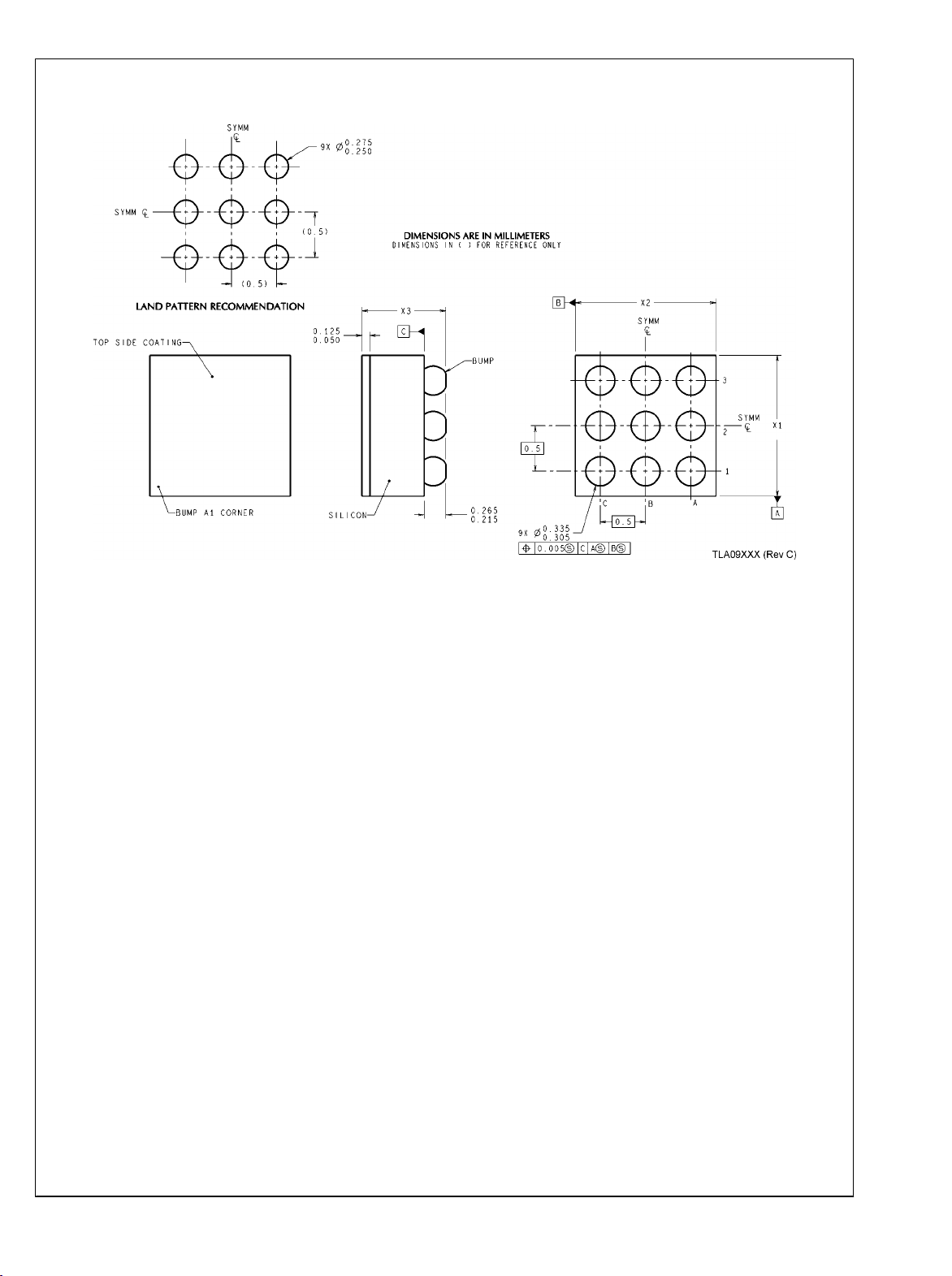
Physical Dimensions inches (millimeters) unless otherwise noted
LM3687
NS Package Number TLA09BBA
The dimensions for X1, X2 and X3 are given as:
9-Bump Thin Micro SMD Package, Large Bump, 0.5mm Pitch
For most accurate revision please refer to www.national.com/packaging/parts/
X1 = 1539µm ± 30µm
X2 = 1539µm ± 30µm
X3 = 600µm ± 75µm
21 www.national.com

Notes
For more National Semiconductor product information and proven design tools, visit the following Web sites at:
Products Design Support
Amplifiers www.national.com/amplifiers WEBENCH www.national.com/webench
Audio www.national.com/audio Analog University www.national.com/AU
Clock Conditioners www.national.com/timing App Notes www.national.com/appnotes
Data Converters www.national.com/adc Distributors www.national.com/contacts
Displays www.national.com/displays Green Compliance www.national.com/quality/green
Ethernet www.national.com/ethernet Packaging www.national.com/packaging
Interface www.national.com/interface Quality and Reliability www.national.com/quality
LVDS www.national.com/lvds Reference Designs www.national.com/refdesigns
Power Management www.national.com/power Feedback www.national.com/feedback
Switching Regulators www.national.com/switchers
LDOs www.national.com/ldo
LED Lighting www.national.com/led
PowerWise www.national.com/powerwise
Serial Digital Interface (SDI) www.national.com/sdi
Temperature Sensors www.national.com/tempsensors
Wireless (PLL/VCO) www.national.com/wireless
THE CONTENTS OF THIS DOCUMENT ARE PROVIDED IN CONNECTION WITH NATIONAL SEMICONDUCTOR CORPORATION
(“NATIONAL”) PRODUCTS. NATIONAL MAKES NO REPRESENTATIONS OR WARRANTIES WITH RESPECT TO THE ACCURACY
OR COMPLETENESS OF THE CONTENTS OF THIS PUBLICATION AND RESERVES THE RIGHT TO MAKE CHANGES TO
SPECIFICATIONS AND PRODUCT DESCRIPTIONS AT ANY TIME WITHOUT NOTICE. NO LICENSE, WHETHER EXPRESS,
IMPLIED, ARISING BY ESTOPPEL OR OTHERWISE, TO ANY INTELLECTUAL PROPERTY RIGHTS IS GRANTED BY THIS
DOCUMENT.
TESTING AND OTHER QUALITY CONTROLS ARE USED TO THE EXTENT NATIONAL DEEMS NECESSARY TO SUPPORT
NATIONAL’S PRODUCT WARRANTY. EXCEPT WHERE MANDATED BY GOVERNMENT REQUIREMENTS, TESTING OF ALL
PARAMETERS OF EACH PRODUCT IS NOT NECESSARILY PERFORMED. NATIONAL ASSUMES NO LIABILITY FOR
APPLICATIONS ASSISTANCE OR BUYER PRODUCT DESIGN. BUYERS ARE RESPONSIBLE FOR THEIR PRODUCTS AND
APPLICATIONS USING NATIONAL COMPONENTS. PRIOR TO USING OR DISTRIBUTING ANY PRODUCTS THAT INCLUDE
NATIONAL COMPONENTS, BUYERS SHOULD PROVIDE ADEQUATE DESIGN, TESTING AND OPERATING SAFEGUARDS.
EXCEPT AS PROVIDED IN NATIONAL’S TERMS AND CONDITIONS OF SALE FOR SUCH PRODUCTS, NATIONAL ASSUMES NO
LIABILITY WHATSOEVER, AND NATIONAL DISCLAIMS ANY EXPRESS OR IMPLIED WARRANTY RELATING TO THE SALE
AND/OR USE OF NATIONAL PRODUCTS INCLUDING LIABILITY OR WARRANTIES RELATING TO FITNESS FOR A PARTICULAR
PURPOSE, MERCHANTABILITY, OR INFRINGEMENT OF ANY PATENT, COPYRIGHT OR OTHER INTELLECTUAL PROPERTY
RIGHT.
LIFE SUPPORT POLICY
NATIONAL’S PRODUCTS ARE NOT AUTHORIZED FOR USE AS CRITICAL COMPONENTS IN LIFE SUPPORT DEVICES OR
SYSTEMS WITHOUT THE EXPRESS PRIOR WRITTEN APPROVAL OF THE CHIEF EXECUTIVE OFFICER AND GENERAL
COUNSEL OF NATIONAL SEMICONDUCTOR CORPORATION. As used herein:
Life support devices or systems are devices which (a) are intended for surgical implant into the body, or (b) support or sustain life and
whose failure to perform when properly used in accordance with instructions for use provided in the labeling can be reasonably expected
to result in a significant injury to the user. A critical component is any component in a life support device or system whose failure to perform
can be reasonably expected to cause the failure of the life support device or system or to affect its safety or effectiveness.
National Semiconductor and the National Semiconductor logo are registered trademarks of National Semiconductor Corporation. All other
brand or product names may be trademarks or registered trademarks of their respective holders.
Copyright© 2008 National Semiconductor Corporation
For the most current product information visit us at www.national.com
National Semiconductor
Americas Technical
Support Center
Email: support@nsc.com
LM3687 Step-Down DC-DC Converter with Integrated Low Dropout Regulator and Startup Mode
www.national.com
Tel: 1-800-272-9959
National Semiconductor Europe
Technical Support Center
Email: europe.support@nsc.com
German Tel: +49 (0) 180 5010 771
English Tel: +44 (0) 870 850 4288
National Semiconductor Asia
Pacific Technical Support Center
Email: ap.support@nsc.com
National Semiconductor Japan
Technical Support Center
Email: jpn.feedback@nsc.com
 Loading...