


LM3595
Parallel White-LED Driver
LM3595 Parallel White-LED Driver
August 2003
General Description
The LM3595 is a parallel white-LED driver that is capable of
driving four white LEDs. It can supply a total output current of
100mA over an input voltage range of 3.0V to 5.5V. The
amount of constant current sourced to the outputs is user
selectable using one external sense resistor.
LM3595 typically draws 0.03µA when placed in shutdown,
and 200µA when operating in the no-load condition. If any of
the outputs are not used, leave the pin(s) unconnected.
Brightness can be controlled by both analog and PWM techniques. A voltage between 0V and 3V may be applied to the
BRGT pin to vary the current. Output current will linearly
track the voltage applied to the BRGT pin. An active-low
level must be present on the BR-ON pin for analog brightness control to be disabled. Alternatively, a PWM signal can
be applied to the EN pin to vary the perceived brightness of
the LED.
The LM3595 uses an active-high enable level. The LM3595
is available in National’s LLP-10 package.
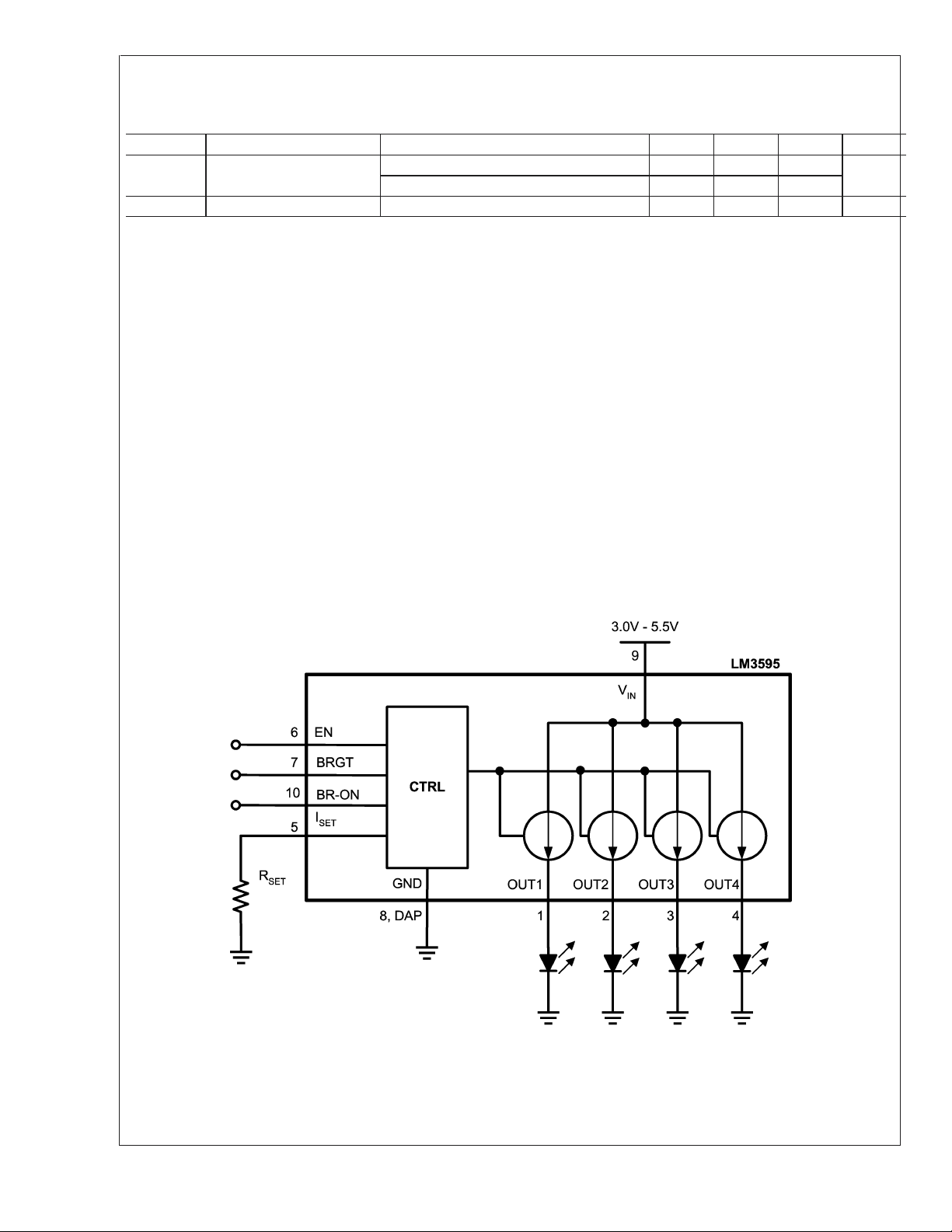
Typical Application Circuit
Features
n Regulated I
current outputs
n Drives one, two, three or four white LED’s with no bias
resistors
n 3.0V to 5.5V Input voltage
n Up to 100mA output current
n Active-High Enable Pin
n Analog Brightness Control
n Very small solution size
n LLP-10 package: 3.0mm x 3.0mm x 0.8mm
n Very Low Shutdown current (0.03µA typ.)
with±0.5% matching between constant
OUT
Applications
n Portable devices using white or blue LEDs with display
and backlight or frontlight
n Keypad LEDs
n Strobe LEDs
20072201
© 2003 National Semiconductor Corporation DS200722 www.national.com

Connection Diagram
LM3595
Pin Description
Pin Name Description
9V
1,2,3,4 OUT1-4 Current Source Outputs 1- 4 - Connect directly to LED’s
5
6
10
7
8, DAP GND Ground
LM3595
10-Pin Leadless Leadframe Package (LLP) - 3mm X 3mm
NS Package Number LDA10A
Input Voltage
Current Set Input- The resistor value tied between this pin and ground sets the
output current.
I
IN
SET
Active-High Enable Input-A1MΩ resistor is connected internally between this
EN
pin and GND to pull the voltage on this pin to 0V, and shut down the part,
when the pin is left floating.
BR-ON
Active-High Analog Brightness Control Enable - A voltage of .65 x V
applied to this pin to enable analog brightness control.
Analog-voltage-controlled Brightness Input - When the BR-ON pin is set high,
BRGT
the voltage on this pin allows analog control of the LED’s brightness. The
recommended voltage range on this pin is0-3Vwhere 3V is V
input impedance of this pin is 300kΩ.
IN
BR(MAX)
20072202
must be
. The
Ordering Information
Order Number Package Number Package Marking Supplied as:
LM3595LD LDA10A L3595 1000 units on Tape-and-Reel
LM3595LDX LDA10A L3595 3500 units on Tape-and-Reel
www.national.com 2

LM3595
Absolute Maximum Ratings (Notes 1,
2)
If Military/Aerospace specified devices are required,
please contact the National Semiconductor Sales Office/
Distributors for availability and specifications.
V
IN
EN, BR-ON, BRGT -0.3V to
Junction Temperature (T
J-MAX-ABS
) 150˚C
Continuous Power Dissiation
(Note 3) Internally Limited
Storage Temperature Range -65˚C to 150˚C
−0.3V to 6.0V
+ 0.3V) w/
(V
IN
6.0V max
Operating Ratings (Notes 1, 2)
Input Voltage Range (Note 5) 3.0V to 5.5V
Output Voltage Range (Note 5) 2.0V to 5.5V
Junction Temperature Range
(Note 6) -40˚C to 105˚C
Ambient Temperature Range
-40˚C to 85˚C
(Note 6)
Thermal Information
Junction-to-Ambient Thermal
Resistance, LLP-10 Package (θ
(Note 7) 55˚C/W
)
JA
Lead Temperature
(Soldering, 5 Sec.) 260˚C
ESD Rating (Note 4)
Human-body model
Machine model
2kV
200V
Electrical Characteristics (Notes 2, 8)
Limits in standard typeface and typical values apply for TJ=25oC. Limits in boldface type apply over the operating junction
temperature range. Unless otherwise specified: V
= 5V, V
IN
Symbol Parameter Conditions Min Typ Max Units
≤ 5.5V
IN
≤ (VIN- 0.7V)
OUTX
= 4.99kΩ
≤ 5.5V
IN
≤ (VIN- 0.42V)
OUTX
= 8.25kΩ
≤ 5.5V
IN
≤ (VIN- 0.28V)
OUTX
= 12.4kΩ
=95%xI
OUT
= 4.99kΩ (I
=95%xI
OUT
= 12.4kΩ (I
= 0mA, V(BR-ON) = VIN,R
= 0mA, V(BR-ON) = VIN,R
I
OUTX
I
OUTX-BRGT
I
OUT-MATCH
V
SET
I
OUTX/ISET
V
HR
I
Q
3.0V ≤ V
2.0V ≤ V
R
SET
Output Current Regulation
(Note 5)
3.0V ≤ V
2.0V ≤ V
R
SET
3.0V ≤ V
2.0V ≤ V
R
SET
Analog Brightness Control
Current Regulation
V(BRGT) = 3.0V, V(BR-ON) = V
V(BRGT) = 0V, V(BR-ON) = V
Current Matching Between
Any Two Outputs
I
Pin Voltage 1.147
SET
Output Current to Current
Set Ratio
I
OUT
Current Source Headroom
Voltage (Note 5)
Quiescent Supply Current
R
SET
I
OUT
R
SET
I
OUTX
Open
I
OUTX
8.25kΩ
I
SD
V
EN-IH
V
EN-IL
V
BRON-IH
V
BRON-IL
Shutdown Supply Current EN = 0, V(BR-ON) = V
EN Input Logic High 3.0V ≤ VIN≤ 5.5V 1.2 V
EN Input Logic Low 3.0V ≤ VIN≤ 5.5V 0 .5 V
BR-ON Input Logic High 3.0V ≤ VIN≤ 5.5V .65xV
BR-ON Input Logic Low 3.0V ≤ VIN≤ 5.5V 0 .35xV
= 3.6V, R
OUTX
IN
IN
(nom)
(nom) approx. 25mA)
OUT
(nom)
(nom) approx. 10mA)
OUT
IN
= 8.25kΩ, V(EN) = VIN, V(BR-ON) = 0V
SET
22.54
(-8%)
13.80
(-8%)
9.20
(-8%)
13.83
(-6.5%)
24.5
15.0
10.0
14.8
100 250 µA
0.5 4 %
(-6%)
95
(-5%)
1.22
100
500 690
200 280
SET
SET
=
=
200 300 µA
350
0.03 1 µA
IN
26.46
(+8%)
16.20
(+8%)
10.80
(+8%)
15.77
(+6.5%)mA(%)
1.293
(+6%)
105
(+5%)
IN
V
IN
IN
mA
(%)
V
(%)
mV
V
V
V
www.national.com3
Electrical Characteristics (Notes 2, 8) (Continued)
Limits in standard typeface and typical values apply for TJ=25oC. Limits in boldface type apply over the operating junction
LM3595
temperature range. Unless otherwise specified: V
Symbol Parameter Conditions Min Typ Max Units
I
EN
I
BR-ON
Note 1: Absolute Maximum Ratings indicate limits beyond which damage to the component may occur. Operating Ratings are conditions under which operation
of the device is guaranteed. Operating Ratings do not imply guaranteed performance limits. For guaranteed performance limits and associated test conditions, see
the Electrical Characteristics tables.
Note 2: All voltages are with respect to the potential at the GND pin.
Note 3: Thermal shutdown circuitry protects the device from permanent damage.
Note 4: The Human body model is a 100pF capacitor discharged through a 1.5kΩ resistor into each pin. The machine model is a 200pF capacitor discharged
directly into each pin. MIL-STD-883 3015.7
Note 5: The operation rating for minimum input voltage, V
must be satisfied for the desired output current to be realized. For more information, see the section on Output Current Capability found in this datasheet.
Note 6: In applications where high power dissipation and/or poor package thermal resistance is present, the maximum ambient temperature may have to be
derated. Maximum ambient temperature (T
dissipation of the device in the application (P
following equation: T
Note 7: Junction-to-ambient thermal resistance (θ
standard JESD51-7. The test board is a 4-layer FR-4 board measuring 102mm x 76mm x 1.6mm with a 2x1 array of thermal vias. The ground plane on the board
is 50mm x 50mm. Thickness of copper layers are 36µm/18µm/18µm/36µm (1.5oz/1oz/1oz/1.5oz). Ambient temperature in simulation is 22˚C, still air. Power
dissipation is 1W. The value of θ
and environmental conditions. In applications where high maximum power dissipation exists (high V
issues. For more information on these topics, please refer to Application Note 1187: Leadless Leadframe Package (LLP) and the Power Dissipation and PCB Layout
Considerations sections of this datasheet.
Note 8: All room temperature limits are 100% tested or guaranteed through statistical analysis. All limits at temperature extremes are guaranteed by correlation
using standard Statistical Quality Control methods (SQC). All limits are used to calculate Average Outgoing Quality Level (AOQL). Typical numbers are not
guaranteed, but do represent the most likely norm.
Note 9: The EN pin has an internally connected 1MΩ pull-down resistor
EN Pin Current (Note 9)
BR-ON Pin Current 0 ≤ V
A-MAX=TJ-MAX-OP
-(θJAxP
of the LM3595 in LLP-10 could fall in a range as wide as 50˚C/W to 150˚C/W (if not wider), depending on PWB material, layout,
JA
V(EN) = 1.5V 1.5
V(EN) = 0V 0
) is dependent on the maximum operating junction temperature (T
A-MAX
), and the junction-to ambient thermal resistance of the part/package in the application (θJA), as given by the
D-MAX
).
D-MAX
) is taken from a thermal modeling result, performed under the conditions and guidelines set forth in the JEDEC
JA
IN
BR-ON
, is limited by V
MIN
= 5V, V
≤ V
IN
OUTX
OUTX
= 3.6V, R
and I
OUTX
= 8.25kΩ, V(EN) = VIN, V(BR-ON) = 0V
SET
0µA
as dictated by headroom voltage. The equation, V
= 105˚C), the maximum power
J-MAX-OP
, high I
IN
), special care must be paid to thermal dissipation
OUT
MIN
≥ (V
OUTX+VHR
µA
),
Block Diagram
20072203
www.national.com 4

LM3595
Typical Performance Characteristics Unless otherwise specified: V
8.25kΩ,EN=V
Output Current vs. Input Voltage Output Current vs. Input Voltage
Output Current vs. Headroom Voltage Output Current vs. Headroom Voltage
IN,TA
= 25˚C
20072207
= 5V, BR-ON = 0V, R
IN
SET
20072210
=
20072206
Output Current vs. Current Set Resistor Quiescent Current vs. Input Voltage (R
20072217
SET
20072213
= Open)
20072211
www.national.com5

Typical Performance Characteristics Unless otherwise specified: V
8.25kΩ,EN=V
LM3595
Output Current vs. Output Voltage I
= 25˚C (Continued)
IN,TA
SET
= 5V, BR-ON = 0V, R
IN
Pin Voltage vs. BRGT Pin Voltage
SET
=
Enable Voltage vs. Input Voltage
20072205
20072209
20072208
www.national.com 6

Detailed Block Diagram
LM3595
20072204
www.national.com7

Circuit Description
The LM3595 is a parallel white-LED driver with four matched
LM3595
current outputs. This part is intended to be driven off of an
existing power supply rail or other regulated voltage source
found within the surrounding system. The matched current
regulators each have a 100:1 current ratio between the
OUTx outputs and the I
currents. The mirrors control the
SET
current through the LEDs without the use of external ballast
resistors. With a total of 100mA of total output current available, the LM3595 is easily capable of supplying 25mA per
each of the four outputs through the proper selection of the
resistor. LED brightness control can be achieved on
R
SET
the LM3595 with a PWM signal and/or an analog voltage.
Application Information
ENABLE / SHUTDOWN
When the voltage on the active-high-logic enable pin is low,
the LM3595 will be in shutdown. While disabled, the LM3595
typically draws 0.1µA. When the EN pin is unconnected, the
part automatically goes into shutdown due to an internal
1MΩ pull-down resistor that is tied between EN and GND.
OUTPUT CURRENT CAPABILITY
The LM3595 is capable of providing up to 25mA of current to
each of the four outputs given an input voltage of 3.0V to
5.5V. The outputs have a typical current matching of 0.5%
between adjacent sources. An external resistor can be used
to set the output current, as approximated with the following
the equation:
=100 x (1.22V / I
R
SET
In order for the output currents to be regulated properly,
sufficient headroom voltage (V
headroom voltage refers to the minimum amount of voltage
that must be present across the current source in order to
ensure the desired current is realizable. To ensure the desired current is obtained, apply the following equations to
find the minimum input voltage required:
V
IN-VOUTX
V
is the diode forward voltage, and VHRis defined by
OUTX
the following equation:
V
HR=kHR
is the desired diode current, and kHR, typically
I
OUTX
23mV/mA in the LM3595, is a proportionality constant that
represents the ON-resistance of the internal current mirror
transistors. For worst-case design calculations, using a k
of 30mV/mA is recommended. (Worst-case recommendation
accounts for parameter shifts from part-to-part variation and
applies over the full operating temperature range). Changes
in headroom voltage from one output to the next, possible
with LED forward voltage mismatch, will result in different
output currents and LED brightness mismatch. Thus, operating the LM3595 with insufficient headroom voltage across
all current sources should be avoided.
) with BR-ON = 0V
OUTX
) must be present. The
HR
≥ V
HR
x (0.95 x I
OUTX
)
TABLE 1. I
OUT,RSET
and V
HR-MIN
Voltage (BR-ON = 0V), kHR= 30 mV/mA (worst-case)
I
OUT
R
SET
V
HEADROOM
10mA 12.4kΩ 285mV
15mA 8.25kΩ 430mV
25mA 4.88kΩ 715mV
PWM BRIGHTNESS CONTROL
Brightness control can be implemented by pulsing a signal at
the EN pin. When a PWM signal is used to drive the EN pin
of the LM3595, the BR-ON pin should be driven low. The
R
value should be selected using the R
SET
SET
equation
when the analog brightness control feature is disabled. LED
brightness is proportional to the duty cycle (D) of the PWM
signal. For linear brightness control over the full duty cycle
adjustment range, the PWM frequency (f) should be limited
to accommodate the turn-on time (T
= 50µs) of the de-
ON
vice.
>
D x (1/f)
f
MAX=DMIN÷TON
T
ON
If the PWM frequency is much less than 100Hz, flicker may
be seen in the LEDs. For the LM3595, zero duty cycle will
turn off the LEDs and a 50% duty cycle will result in an
average I
example, if R
will result in an average I
programmed LED current. R
being half of the programmed LED current. For
OUT
is set to program 15mA, a 50% duty cycle
SET
of 7.5mA. I
LED
SET
being half the
OUT
should be chosen not to
exceed the maximum current delivery capability of the device.
ANALOG BRIGHTNESS CONTROL
The LM3595 allows for analog brightness control using the
BR-ON, and BRGT pin. To enable this function, the BR-ON
pin must be set to a voltage greater or equal to 0.45*V
.
IN
With analog brightness enabled, the voltage delivered to pin
BRGT can be used to adjust the output currents. Use the
maximum desired current (I
OUTX(max)
analog voltage to be used in the adjustment (V(BR)
size R
HR
Table 2 shows the current through each LED for the LM3595
according to the following equation:
SET
) and the maximum
)to
(max)
with various BRGT and RSET values.
When analog brightness is used, applying 0V to the BRGT
pin does not turn the LEDs off completely. There is a small
amount of leakage current (100µA) that typically causes a
small amount of light to be emitted from the LED. In order to
completely turn off the LEDs, drive the EN pin low to disable
the part.
www.national.com 8
Application Information (Continued)
LM3595
TABLE 2. LED Current when using the BRGT input with BR-ON = V
R
(Ω) 4.99kΩ 6.25kΩ 8.25kΩ 12.4kΩ
SET
VBRGT(V) I
(mA) I
LED
0.0 0.1 0.1 0.1 0.1
0.5 4.1 3.3 2.5 1.6
1.0 8.1 6.7 4.9 3.3
1.5 12.2 10.0 7.4 4.9
2.0 16.3 13.3 9.9 6.6
2.5 20.4 16.7 12.3 8.2
3.0 24.5 20.0 14.8 9.8
LED SELECTION
The LM3595 is designed to drive white-LEDs with a typical
forward voltage of 3.0V to 4.0V. The maximum LED forward
voltage that the LM3595 can accommodate is highly dependant upon V
Capability for more information on finding maximum V
IN
and I
. (See the section on Output Current
OUTX
OUTX
For applications that demand color and brightness matching,
care must be taken to select LEDs from the same chromaticity group. Forward current matching is assured over the
LED process variations due to the constant current outputs
of the LM3595.
TABLE 3. White LED Selection:
Component Manufacture Contact
Manufacturer Contact
Osram www.osram-os.com
Nichia www.nichia.com
(mA) I
LED
parallel connected LEDs. For example, if 30mA is the desired drive current for 2 parallel connected LEDs, R
V
BRGT
the outputs is 15mA. Other combinations of parallel outputs
may be implemented in similar fashions, such as in Figure 2.
.)
IN
(mA) I
LED
LED
(mA)
SET
and
should be selected so that the current through each of
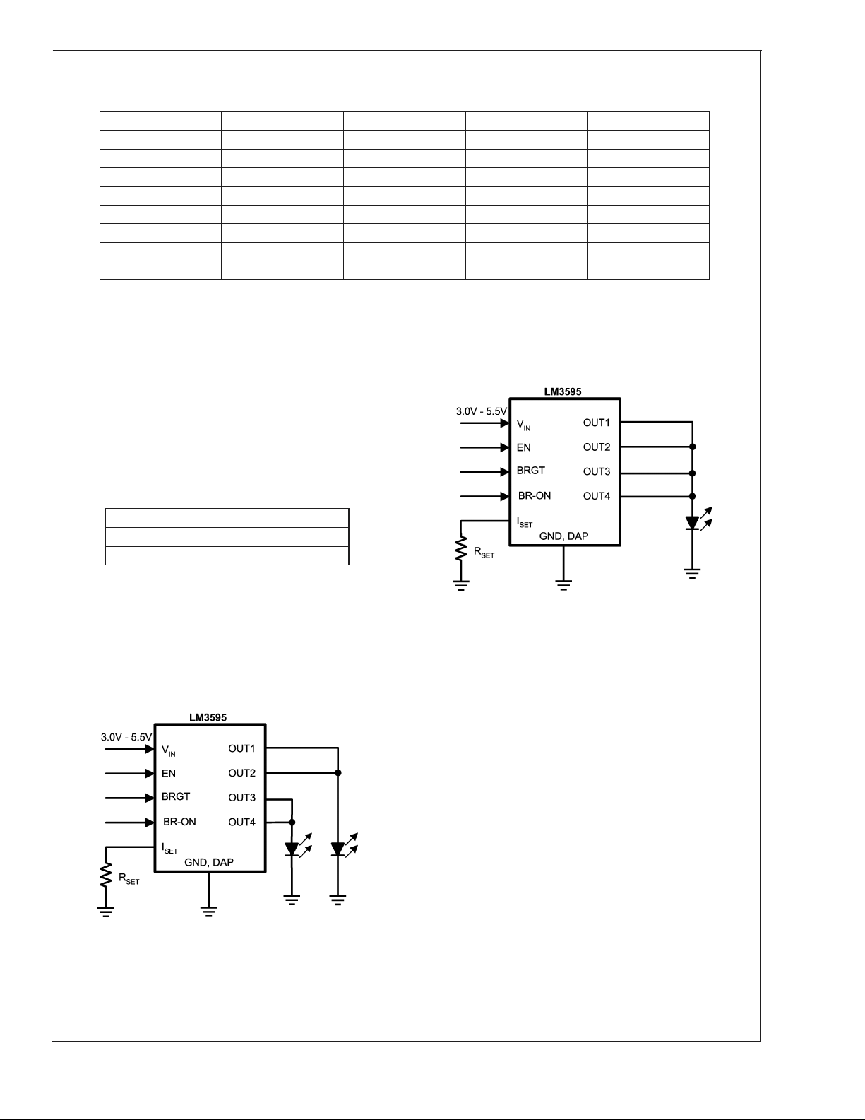
PARALLEL OUTx OUTPUTS FOR INCREASED CURRENT DRIVE
Outputs OUT1 through OUT4 may be connected together in
any combination to drive higher currents through fewer
LEDs. For example in Figure 1, outputs OUT1 and OUT2 are
connected together to drive one LED while OUT3 and OUT4
are connected together to drive a second LED.
20072215
FIGURE 1. Two Parallel Connected LEDs
With this configuration, two parallel current sources of equal
value provide current to each LED. R
SET
and V
BRGT
should
therefore be chosen so that the current through each output
is programmed to 50% of the desired current through the
20072216
FIGURE 2. One Parallel Connected LED
Connecting outputs in parallel does not affect internal operation of the LM3595 and has no impact on the Electrical
Characteristics and limits previously presented. The available diode output current, maximum diode voltage, and all
other specifications provided in the Electrical Characteristics
table apply to parallel output configurations, just as they do
to the standard 4-LED application circuit.
POWER DISSIPATION
The maximum allowable power dissipation that this package
is capable of handling can be determined as follows:
=(T
P
DMax
Where T
is the maximum junction temperature, TAis the
JMAX
ambient temperature, and θ
JMax-TA
)/θ
JA
is the junction-to-ambient
JA
thermal resistance of the specified package. The LM3595
come in the LLP-10 package that has a junction-to-ambient
thermal resistance (θ
) equal to 55˚C/W. This value of θJAis
JA
highly dependant upon the layout of the PC board (See the
PCB Layout Considerations section of this datasheet for
more information). The actual power dissipated by the
LM3595 follows the equation:
=(VINxIIN) - N(V
P
DISS
OUTXxIOUTX
Where N equals the number of active outputs, V
LED forward voltage, and I
is the current supplied to the
OUTX
)
OUTX
is the
www.national.com9

Application Information (Continued)
diode by the LM3595. Power dissipation must be less than
LM3595
that allowed by the package. Please refer to the Absolute
Maximum Rating of the LM3595.
power dissipation. The device will recover and operate normally when the junction temperature falls below the maximum operating junction temperature of 105˚C. It is important
to have good thermal conduction with a proper layout to
reduce thermal resistance.
INPUT CAPACITOR SELECTION
The LM3595 is designed to run off of a fixed input voltage.
Depending on the stability and condition of this voltage rail, it
may be necessary to add a small input capacitor to help filter
out any noise that may be present on the line. In the event
that filtering is needed, surface-mount multi-layer ceramic
capacitors are recommended. These capacitors are small
and inexpensive. A capacitance of 1µF is typically sufficient.
THERMAL PROTECTION
The LM3595 has internal thermal protection circuitry to disable the part if the junction temperature exceeds 150˚C. This
feature will protect the device from damage due to excessive
PCB LAYOUT CONSIDERATIONS
The LLP is a leadframe based Chip Scale Package (CSP)
with very good thermal properties. This package has an
exposed DAP (die attach pad) at the center of the package
measuring 2.0mm x 1.2mm. The main advantage of this
exposed DAP is to offer lower thermal resistance when it is
soldered to the thermal land on the PCB. For PCB layout,
National highly recommends a 1:1 ratio between the package and the PCB thermal land. To further enhance thermal
conductivity, the PCB thermal land may include vias to a
ground plane. For more detailed instructions on mounting
LLP packages, please refer to National Semiconductor Application Note AN-1187.
www.national.com 10

Physical Dimensions inches (millimeters) unless otherwise noted
LM3595 Parallel White-LED Driver
LIFE SUPPORT POLICY
NATIONAL’S PRODUCTS ARE NOT AUTHORIZED FOR USE AS CRITICAL COMPONENTS IN LIFE SUPPORT
DEVICES OR SYSTEMS WITHOUT THE EXPRESS WRITTEN APPROVAL OF THE PRESIDENT AND GENERAL
COUNSEL OF NATIONAL SEMICONDUCTOR CORPORATION. As used herein:
1. Life support devices or systems are devices or
systems which, (a) are intended for surgical implant
into the body, or (b) support or sustain life, and
whose failure to perform when properly used in
accordance with instructions for use provided in the
2. A critical component is any component of a life
support device or system whose failure to perform
can be reasonably expected to cause the failure of
the life support device or system, or to affect its
safety or effectiveness.
labeling, can be reasonably expected to result in a
significant injury to the user.
National Semiconductor
Americas Customer
Support Center
Email: new.feedback@nsc.com
Tel: 1-800-272-9959
www.national.com
National does not assume any responsibility for use of any circuitry described, no circuit patent licenses are implied and National reserves the right at any time without notice to change said circuitry and specifications.
National Semiconductor
Europe Customer Support Center
Fax: +49 (0) 180-530 85 86
Email: europe.support@nsc.com
Deutsch Tel: +49 (0) 69 9508 6208
English Tel: +44 (0) 870 24 0 2171
Français Tel: +33 (0) 1 41 91 8790
National Semiconductor
Asia Pacific Customer
Support Center
Email: ap.support@nsc.com
National Semiconductor
Japan Customer Support Center
Fax: 81-3-5639-7507
Email: jpn.feedback@nsc.com
Tel: 81-3-5639-7560
 Loading...