

LM3590
Series White LED Driver
LM3590 Series White LED Driver
November 2003
General Description
The LM3590 is a White LED constant current driver capable
of supplying up to 3 White LEDs connected in series with
20mA. This device operates over a wide 6V-12.6V input
voltage range. The output can accomodate LEDs with a
combined forward voltage of up to 11.5V, from a 12V input
supply. The LED drive current is programmed by using an
external resistor on the I
LED brightness can be linearly varied up to the programmed
LED current by applying a Pulse Width Modulated (PWM)
signal to the EN pin of the device. The LED output current of
the LM3590 is tightly controlled over temperature and voltage. LED Current matching is guaranteed due to the series
configuration of the LEDs. The series topology also simplifies the connection between the White LEDs in the display
module and the LM3590 since only one connection is required.
The LM3590 typically draws only 50µA when operating in the
no-load condition and draws less than 0.1µA when the device is shut down.
The LM3590 is available in a small 5-pin SOT23 package.
SET
pin.
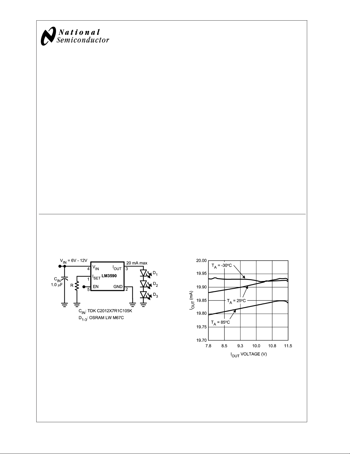
Typical Application Circuit
Features
n Drives up to 3 stacked white LEDs
n 6.0V-12.6V input voltage range
n Up to 20mA LED output current
n Excellent LED current matching guaranteed by series
configuration
n Single connection to the White LEDs in the display
module
n Tightly controlled programmable current source
n Low shutdown current (0.1µA typ.)
n PWM brightness control
n Very small solution size
n SOT23-5 package: 3mm x 3mm x 1.0mm (LxWxH)
Applications
n White LED Display Backlights
n Keypad Backlights
n General purpose constant current driver for high
forward-voltage LEDs
20081301
20081305
© 2003 National Semiconductor Corporation DS200813 www.national.com

Connection Diagram
LM3590
Ordering Information
Order Number Package Description Package Marking Supplied As
LM3590MF SOT23-5 SABB
LM3590MFX SOT23-5 SABB
Pin Description
#
Pin
1I
2 GND Ground Connection
3I
4V
5 EN Device Enable
20081302
¢Z¢1¢
*
¢Z¢1¢
*
Name Function
SET
Programmable LED current Input. The LED current has the following relationship with the
resistor used:
OUT
= 100 x (125 ÷ I
R
SET
Constant Current LED Output
IN
Power Supply Voltage Input. Input voltage range: 6V-12.6V
OUT
)
Tape and Reel
X 250 Units, Tape
and Reel
X 3000 Units, Tape
and Reel
www.national.com 2

LM3590
Absolute Maximum Ratings (Notes 1,
2)
If Military/Aerospace specified devices are required,
please contact the National Semiconductor Sales Office/
Distributors for availability and specifications.
V
IN
EN −0.3 to (V
−0.3 to 13.0V Max
+0.3V) w/
IN
13.0V max
Operating Conditions
Input Voltage Range 6.0V to 12.6V
EN Voltage Range 0V to V
Ambient Temperature (TA)
Range
(Note 4)
Junction Temperature (T
Range
)
J
−40˚C to +85˚C
−40˚C to +110˚C
Maximum Junction Temperature
) 150˚C
(T
JMAX
Storge Temperature −65˚C to +150˚C
Maximum Lead Temperature
260˚C
(Soldering, 5 sec.)
ESD Rating (Note 3)
Thermal Information
Junction-to-Ambient Thermal
Resistance,
SOT23-5 Package (θ
) (Note 5) 220˚C/W
JA
Human Body Model 1.5kV
Machine Model 200V
Electrical Characteristics (Notes 2, 6)
Limits in standard typeface are for TJ= 25˚C and limits in boldface type apply over the full Operating Junction Temperature
Range (−40˚C ≤ T
≤ +110˚C). Unless otherwise specified, CIN= 1 µF, VIN= 12.0V, VEN= 3.0V, R
J
10.8V.
Symbol Parameter Conditions Min Typ Max Units
I
OUT
Output Current Capability VIN= 12V
7.5V ≤ V
V
= 10.8V
IOUT
11.3V ≤ V
R
= 8.35kΩ 15
SET
R
= 12.5kΩ 10
SET
IOUT
IN
≤ 11.5V
≤ 12.6V
19
(−5%)
19
(−5%)
Output Current Programming 125 ÷
I
ratio to I
OUT
I
Q
I
SD
V
ISET
V
HR
Quiescent Supply Current 11.3V ≤ VIN≤ 12.6V
Shutdown Supply Current VIN= 12.6V
I
Reference Voltage 1.25 V
SET
Minimum Current Source
Voltage Headroom (V
V
IOUT
V
IH
V
IL
I
EN
t
ON
Note 1: Absolute Maximum Ratings indicate limits beyond which damage to the device may occur. Operating Ratings are conditions under which operation of the
device is guaranteed. Operating Ratings do not imply guaranteed performance limits. For guaranteed performance limits and associated test conditions, see the
Electrical Characteristics table.
Note 2: All voltages are with respect to the potential at the GND pin.
Note 3: The human-body model is a 100pF capacitor discharged through a 1.5kΩ resistor into each pin. The machine model is a 220pF capacitor discharged
directly into each pin.
Note 4: Maximum ambient temperature (T
dissipation of the device in the application (P
following equation: T
outside the listed T
Note 5: Junction-to-ambient thermal resistance is highly application and board-layout dependent. In applications where high maximum power dissipation exists,
special care must be paid to thermal dissipation issues. For more information on these topics, please refer to the Power Dissipation section of this datasheet.
Logic Input EN: High level 1.1 V
Logic Input EN: Low level 0 0.3 V
Enable Pin Input Current(Note 8) 6 µA
Turn-On Time I
A-MAX=TJ-MAX-OP
rating, so long as the junction temperature of the device does not exceed the maximum operating rating of 110oC.
A
)(Note 7)
SET
= OPEN
R
SET
= OPEN
I
OUT
=0V
V
EN
= 95% nominal 300 mV
I
OUT
−
IN
= 90% of steady state 50 µs
OUT
) is dependent on the maximum operating junction temperature (T
A-MAX
), and the junction-to-ambient thermal resistance of the part/package in the application (θJA), as given by the
D-MAX
-(θJAxP
). The ambient temperature operating rating is provided merely for convenience. This part may be operated
D-MAX
J-MAX-OP
= 6.19kΩ,V
SET
IOUT
20 21
(+5%)
20 21
(+5%)
R
SET
100:1
50 75 µA
0.1 1 µA
IN
=110oC), the maximum power
IN
=
mA
A
V
www.national.com3

Electrical Characteristics (Notes 2, 6) (Continued)
Note 6: All room temperature limits are 100% tested or guaranteed through statistical analysis. All limits at temperature extremes are guaranteed by correlation
LM3590
using standard Statistical Quality Control methods (SQC). All limits are used to calculate Average Outgoing Quality Level (AOQL). Typical numbers are not
guaranteed, but do represent the most likely norm.
Note 7: The current source is connected internally between V
For the current source to regulate properly, a minimum headroom voltage must be present across it. Minimum required headroom voltage is proportional to the
current flowing through the current source, as dictated by this equation: V
Note 8: An internal 500kΩ pull-down resistor is connected between the EN and GND pins.
IN
and V
. The voltage across the current source, [VIN−V
IOUT
HR-MIN
= 300mV x (I
OUT
÷ 20mA).
], is referred to as headroom voltage.
IOUT
Functional Block Diagram
www.national.com 4
20081314

LM3590
Typical Performance Characteristics Unless otherwise specified, C
3.0V, V
IOUT
= 10.8V, R
= 6.19kΩ,TA= 25˚C. CINis a low ESR multi-layer ceramic capacitor (MLCC).
SET
I
I
OUT
OUT
vs V
vs R
IN
20081304
SET
I
OUT
= 1µF, VIN= 12.0V, VEN=
IN
vs V
IOUT
IQvs V
IN
20081305
20081306
V
SET
vs V
IN
20081308
Shutdown Supply Current vs V
20081307
IN
20081309
www.national.com5

Typical Performance Characteristics Unless otherwise specified, C
3.0V, V
LM3590
IOUT
= 10.8V, R
Shutdown Threshold vs V
= 6.19kΩ,TA= 25˚C. CINis a low ESR multi-layer ceramic capacitor (MLCC). (Continued)
SET
IN
20081310
= 1µF, VIN= 12.0V, VEN=
IN
Startup
20081311
www.national.com 6

Application Information
CIRCUIT DESCRIPTION
The LM3590 is a constant current series White-LED Driver,
providing up to 20mA from an input voltage between 7.5V to
12.6V. To set the LED drive current, the LM3590 uses a
resistor connected to the I
This reference current is then multiplied and mirrored to the
constant current output, I
controlled by applying a PWM (Pulse Width Modulation)
signal to the Enable pin (EN). (see PWM BRIGHTNESS
CONTROL PROCEDURES section).
ENABLE MODE
The Enable pin (EN) disables the part and reduces the
quiescent current to 0.1µA (typ.). The LM3590 has an activehigh enable pin (LOW = shut down, HIGH = operating). The
LM3590 EN pin can be driven with a low-voltage CMOS logic
signal (1.5V logic, 1.8V logic, etc). There is an internal
500kΩ pull-down between the EN and GND pins of the
LM3590.
CAPACITOR SELECTION
Although not required for normal operation, a capacitor can
be added to the voltage input of the LM3590 to reduce line
noise. A surface-mount multi-layer ceramic capacitor
(MLCC) is recommended. MLCCs are small, inexpensive
and have very low equivalent series resistance (ESR,
≤15mΩ typ.). MLCCs with a X5R or X7R temperature characteristic are preferred for use with the LM3590. Table 1.
Ceramic Capacitor Manufacturers lists suggested capacitor
suppliers for the typical application circuit.
pin to set a reference current.
SET
. The LED brightness can be
OUT
required headroom voltage is proportional to the current
flowing through the current source, as dictated by the equation:
V
HR-MIN=kHRxIOUT
The parameter kHR, typically 15mV/mA in the LM3590, is a
proportionality constant that represents the ON-resistance of
the internal current mirror transistors. For worst-case design
calculations, using a k
of 20mV/mA is recommended.
HR
(Worst-case recommendation accounts for parameter shifts
from part-to-part variation and applies over the full operating
temperature range). Figure 1 shows how output current of
the LM3590 varies with respect to headroom voltage.
LM3590
TABLE 1. Ceramic Capacitor Manufacturers
Manufacturer Contact
TDK www.component.tdk.com
Murata www.murata.com
Taiyo Yuden www.t-yuden.com
LED SELECTION
The LM3590 is designed to drive up to 3 LEDs with the
combined forward voltages of the LEDs being no greater
than 11.5V, when using a 12V input supply. The typical and
maximum diode forward voltage depends highly on the
manufacturer and their technology. Table 2. White LED Se-
lection lists two suggested manufacturers. LED Forward current matching is guaranteed by design, due to the series
LED configuration of the LM3590.
TABLE 2. White LED Selection
Manufacturer Contact
Osram www.osram-os.com
Nichia www.nichia.com
LED HEADROOM VOLTAGE (V
)
HR
A single current source is connected internally between V
and I
V
. The voltage across the current source, (VIN−
OUT
), is referred to as headroom voltage (VHR). The cur-
IOUT
rent source requires a sufficient amount of headroom voltage
to be present across it in order to regulate properly. Minimum
20081312
FIGURE 1. I
VHR=VIN−V
OUT
vs V
IOUT
HR
VIN= 12.0V
On the flat part of the graph, the current is regulated properly
as there is sufficient headroom voltage for regulation. On the
sloping part of the graph the headroom voltage is too small,
the current source is squeezed, and the current drive capability is limited. Thus, operating the LM3590 with insufficient
headroom voltage across the current source should be
avoided.
PIN
I
SET
An external resistor, R
, connected to the I
SET
pin sets the
SET
output current. The internal current mirror sets the series
LED output current with a 100:1 ratio to the current through
. The current matching through each LED is guaranteed
R
SET
by the series LED drive topology. The following equation
approximates the LED current:
= 100 x (1.25V ÷ R
I
OUT
SET
) (Amps)
PWM BRIGHTNESS CONTROL PROCEDURES
The brightness of the LEDs can be linearly varied from zero
up to the maximum programmed current level by applying a
IN
Pulse-Width-Modulated signal to the EN pin of the LM3590.
The following procedures illustrate how to program the LED
drive current and adjust the output current level using a
PWM signal.
1. Determine the maximum desired I
equation to calculate R
I
OUT
SET
current. Use the
OUT
www.national.com7

Application Information (Continued)
2. Brightness control can be implemented by pulsing a
LM3590
signal at the EN pin. LED brightness is proportional to
the duty cycle (D) of the PWM signal. For linear brightness control over the full duty cycle adjustment range,
the PWM frequency (f) should be limited to accommodate the turn-on time (T
D x (1/f)
f
MAX=DMIN÷TON
= 50µs) of the device.
ON
>
T
ON
If the PWM frequency is much less than 100Hz, flicker
may be seen in the LEDs. For the LM3590, zero duty
cycle will turn off the LEDs and a 50% duty cycle will
result in an average I
LED current. For example, if R
being half of the programmed
OUT
is set to program
SET
15mA, a 50% duty cycle will result in an average I
7.5mA.
POWER DISSIPATION
The power dissipation (P
) can be approximated with the equations below. P
ture (T
J
DISSIPATION
) and junction tempera-
is the product of the input current and input voltage, P
Application Circuits
Figure 2 shows how to program the LED current to four
different DC levels using two digital logic signals. The programmed LED current is a function of the equivalent resis-
LED
IOUT
the power consumed by the LEDs, T
perature, and θ
is the junction-to-ambient thermal resis-
JA
tance for the SOT23-5 package. V
the LM3590, V
LEDs connected to the I
is the sum of the forward voltages of
IOUT
OUT
pin, and I
is the ambient tem-
A
is the input voltage to
IN
is the programmed
OUT
LED current.
P
DISSIPATION=PIN-PIOUT
=(VINxI
T
J=TA
OUT
+(P
)−(V
IOUTxIOUT
DISSIPATION
)
x θJA)
The junction temperature rating takes precedence over the
ambient temperature rating. The LM3590 may be operated
outside the ambient temperature rating, so long as the junction temperature of the device does not exceed the maximum operating rating of 110˚C. The maximum ambient tem-
of
perature rating must be derated in applications where high
power dissipation and/or poor thermal resistance causes the
junction temperature to exceed 110˚C.
IN
is
tance on the I
SET
pin (R
), resulting from the logic signals
ISET
on SET1 and SET2. Example values for R1, R2, and RSET
an the resulting 4 current levels are shown below.
FIGURE 2. Example: R1= 15.8kΩ,R2= 31.6kΩ,R
TABLE 3. Digital LED Current Programming
EN SET1 SET2 R
ISET
0 X X Shutdown Shutdown Shutdown
111 R
110 R
101 R
100 R
www.national.com 8
SETiR1iR2
SETiR1
SETiR2
SET
20081313
= 31.6kΩ
SET
Example R
ISET
Example I
31.6kΩi15.kΩi31.6kΩ 16mA
31.6kΩi15.kΩ 12mA
31.6kΩi31.6kΩ 8mA
31.6kΩ 4mA
OUT

Physical Dimensions inches (millimeters) unless otherwise noted
LM3590 Series White LED Driver
5 Lead Small Outline Package (SOT23-5)
NS Package Number MF05A
LIFE SUPPORT POLICY
NATIONAL’S PRODUCTS ARE NOT AUTHORIZED FOR USE AS CRITICAL COMPONENTS IN LIFE SUPPORT
DEVICES OR SYSTEMS WITHOUT THE EXPRESS WRITTEN APPROVAL OF THE PRESIDENT AND GENERAL
COUNSEL OF NATIONAL SEMICONDUCTOR CORPORATION. As used herein:
1. Life support devices or systems are devices or
systems which, (a) are intended for surgical implant
into the body, or (b) support or sustain life, and
whose failure to perform when properly used in
accordance with instructions for use provided in the
2. A critical component is any component of a life
support device or system whose failure to perform
can be reasonably expected to cause the failure of
the life support device or system, or to affect its
safety or effectiveness.
labeling, can be reasonably expected to result in a
significant injury to the user.
BANNED SUBSTANCE COMPLIANCE
National Semiconductor certifies that the products and packing materials meet the provisions of the Customer Products
Stewardship Specification (CSP-9-111C2) and the Banned Substances and Materials of Interest Specification
(CSP-9-111S2) and contain no ‘‘Banned Substances’’ as defined in CSP-9-111S2.
National Semiconductor
Americas Customer
Support Center
Email: new.feedback@nsc.com
Tel: 1-800-272-9959
www.national.com
National does not assume any responsibility for use of any circuitry described, no circuit patent licenses are implied and National reserves the right at any time without notice to change said circuitry and specifications.
National Semiconductor
Europe Customer Support Center
Fax: +49 (0) 180-530 85 86
Email: europe.support@nsc.com
Deutsch Tel: +49 (0) 69 9508 6208
English Tel: +44 (0) 870 24 0 2171
Français Tel: +33 (0) 1 41 91 8790
National Semiconductor
Asia Pacific Customer
Support Center
Email: ap.support@nsc.com
National Semiconductor
Japan Customer Support Center
Fax: 81-3-5639-7507
Email: jpn.feedback@nsc.com
Tel: 81-3-5639-7560
 Loading...