

LM3543
Triple Port USB Power Distribution Switch and
Over-Current Protection
LM3543 Triple Port USB Power Distribution Switch and Over-Current Protection
June 2005
General Description
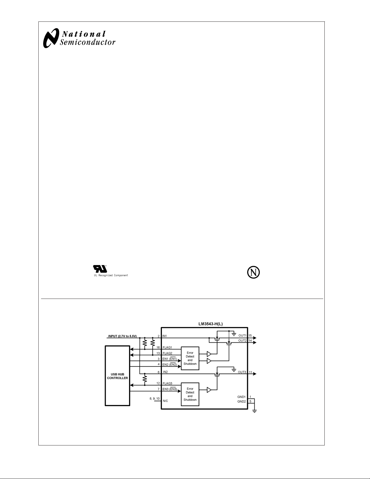
The LM3543 is a triple high-side power switch that is an
excellent choice for use in Root, Self-Powered and BusPowered USB (Universal Serial Bus) Hubs. Independent
port enables, flag signals to alert USB controllers of error
conditions, controlled start-up in hot-plug events, and short
circuit protection all satisfy USB requirements.
The LM3543 accepts input voltages between 2.7V and 5.5V.
The Enable logic inputs, available in active-high and activelow versions, can be powered off any voltage in the 2.7V to
5.5V range. The LM3543 limits the continuous current
through a single port to 1.25A (max.) when it is shorted to
ground.
The low on-state resistance of the LM3543 switches ensures
the LM3543 will satisfy USB voltage drop requirements,
even when current through a switch reaches 500 mA. Thus,
High-Powered USB Functions, Low-Powered USB Functions, and Bus-Powered USB Hubs can all be powered off a
Root or Self-Powered USB Hub containing the LM3543.
Added features of the LM3543 include current foldback to
reduce power consumption in current overload conditions,
thermal shutdown to prevent device failure caused by highcurrent overheating, and undervoltage lockout to keep
switches from operating if the input voltage is below acceptable levels.
Features
n Compatible with USB1.1 and USB 2.0
n 90mΩ (typ.) High-Side MOSFET Switch
n 500mA Continuous Current per Port
n 7 ms Fault Flag Delay Filters Hot-Plug Events
n Industry Standard Pin Order
n Short Circuit Protection with Power-Saving Current
Foldback
n Thermal Shutdown Protection
n Undervoltage Lockout
n Recognized by UL and Nemko
n Input Voltage Range: 2.7V to 5.5V
n 5 µA Maximum Standby Supply Current
n 16-Pin SOIC Package
n Ambient Temperature Range: −40˚C to 85˚C
Applications
n USB Root, Self-Powered, and Bus-Powered Hubs
n USB Devices such as Monitors and Printers
n General Purpose High Side Switch Applications
10125832
10125833
Functional Diagram
10125801
© 2005 National Semiconductor Corporation DS101258 www.national.com
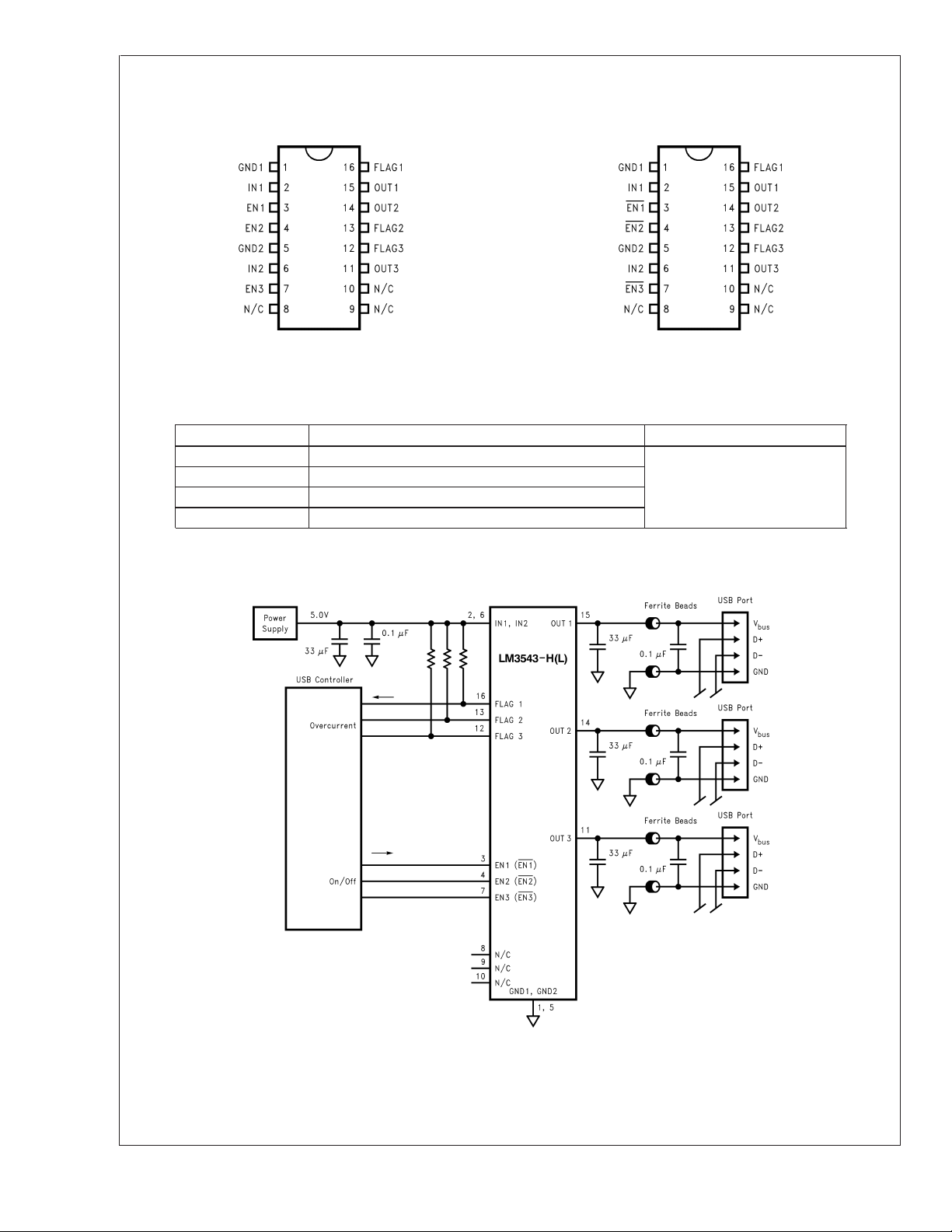
Connection Diagrams
LM3543
LM3543-H
16-Pin SOIC
LM3543-L
16-Pin SOIC
Top View
10125802
Ordering Information
Part Number Enable, Delivery Option Package Type
LM3543M-H Active High Enable
LM3543M-L Active Low Enable
LM3543MX-H Active High Enable, 2500 units per reel
LM3543MX-L Active Low Enable, 2500 units per reel
Typical Application Circuit
Top View
10125829
SO-16
NS Package Number M16A
FIGURE 1. The LM3543 used in a Self-Powered or Root USB Hub
www.national.com 2
10125804
LM3543
Absolute Maximum Ratings (Note 1)
If Military/Aerospace specified devices are required,
please contact the National Semiconductor Sales Office/
Lead Temperature Range
(Soldering, 5 sec.) 260˚C
ESD Rating (Note 3) 2 kV
Distributors for availability and specifications.
Voltage at IN
Voltage at EN
pins
Power Dissipation (Note 2) Internally Limited
and OUTXpins −0.3V to 6V
X
(ENX) and FLAG
X
X
−0.3V to 5.5V
Operating Ratings
Supply Voltage Range 2.7V to 5.5V
Continuous Output Current Range
(Each Output) 0 mA to 500 mA
Maximum Junction Temperature 150˚C
Junction Temperature Range −40˚C to 125˚C
Storage Temperature Range −65˚C to 150˚C
DC Electrical Characteristics
Limits in standard typeface are for TJ= 25˚C, and limits in boldface type apply over the full operating temperature range. Unless otherwise specified: V
Symbol Parameter Conditions Min Typ Max Units
R
I
ON
OUT
On Resistance
OUTXContinuous Output
Current
I
LEAK-OUT
I
SC
OUTXLeakage Current ENX= 0 (ENX=VIN);
OUTXShort-Circuit Current
(Note 4)
OC
THRESH
V
L_FLAG
I
LEAK-FLAG
I
LEAK-EN
V
IH
V
IL
V
UVLO
I
DDON
I
DDOFF
Note 1: Absolute Maximum Ratings indicate limits beyond which damage to the device may occur. Electrical specifications do not apply when operating the device
beyond its rated operating conditions.
Note 2: The maximum allowable power dissipation is a function of the Maximum Junction Temperature (T
the Ambient Temperature (T
at any temperature is P
thermal shutdown.
Note 3: The Human body model is a 100 pF capacitor discharged through a 1.5 kΩ resistor into each pin.
Note 4: Thermal Shutdown will protect the device from permanent damage.
Overcurrent Threshold 2.0 3.2 A
FLAGXOutput-Low Voltage I(FLAGX)=10mA 0.1 0.3 V
FLAGXLeakage Current 2.7 ≤ V
ENxInput Leakage Current ENx/ENx=0Vor
EN/EN Input Logic High 2.7V ≤ VIN≤ 5.5V 2.4 V
EN/EN Input Logic Low 4.5V ≤ VIN≤ 5.5V 0.8 V
Under-Voltage Lockout
Threshold
Operational Supply Current
Shutdown Supply Current
MAX
= 5.0V, ENX=VIN(LM3543-H) or ENX= 0V (LM3543-L).
IN
V
IN
V
IN
= 5V, I
= 3.3V, I
= 0.5A 90 125
OUTX
OUTX
3.0V ≤ VIN≤ 5.5V 0.5 A
TJ= 25˚C
EN
= 0 (ENX=VIN);
X
−40≤ TJ≤ 85˚C
OUTXConnected to GND 0.8 1.25 A
≤ 5.5V 0.2 1 µA
FLAG
ENx/ENx=V
2.7V ≤ V
EN
x=VIN
IN
≤ 4.5V 0.4
IN
(ENx=0);
TJ= 25˚C
EN
x=VIN
(ENx=0);
−40˚C ≤ TJ≤ 125˚C
= 0 (ENx=VIN);
EN
x
TJ= 25˚C
−40˚C ≤ T
). The LM3543 in the 16-pin SOIC package has a T
A
=(T
)/θJA. Exceeding the maximum allowable power dissipation will cause excessive die temperature, and the part will go into
JMAX−TA
≤ 125˚C 5 µA
J
of 150˚C and a θJAof 130˚C/W. The maximum allowable power dissipation
JMAX
= 0.5A 95 130
0.01 1 µA
10 µA
−0.5 0.5 µA
1.8 V
375 600 µA
800 µA
1µA
), Junction to Ambient Thermal Resistance (θJA), and
JMAX
mΩ
www.national.com3
AC Electrical Characteristics
Limits are for TJ= 25˚C and VIN= 5.0V.
LM3543
Symbol Parameter Conditions Min Typ Max Units
t
r
t
f
t
ON
t
OFF
t
F
Note 5: Time for OUTxto rise from 10% to 90% of its enabled steady-state value after ENx(ENx) is asserted.
Note 6: Time for OUTxto fall from 10% to 90% of its enabled steady-state value after ENx(ENx) is deasserted.
Note 7: Time between ENxrising through VIH(ENxfalling through VIL) and OUTxrising through 90% of its enabled steady-state voltage.
Note 8: Time between ENxfalling through VIL(ENxrising through VIH) and OUTxfalling through 10% of its enabled steady-state voltage.
Note 9: Time between ENxrising through VIN(ENxfalling through VIN) and FLAGXfalling through 0.3V when OUTXis connected to GND.
OUTxRise Time (Note 5) CL= 33 µF, I
OUTxFall Time (Note 6) CL= 33 µF, I
Turn-on Delay (Note 7) CL= 33 µF, I
Turn-off Delay (Note 8) CL= 33 µF, I
Flag Delay (Note 9) I
=10mA 7 ms
FLAG
= 500mA 1.5 ms
LOAD
= 500mA 0.9 ms
LOAD
= 500mA 2.9 ms
LOAD
= 500mA 0.7 ms
LOAD
Pin Descriptions
Pin Number Pin Name Pin Function
2, 6 IN 1, 2 Supply Inputs: These pins are the inputs to the power switches and the supply
input for the IC. In most applications they are connected together externally
and to a single input voltage supply.
1, 5 GND 1, 2 Grounds: Must be connected together and to a common ground.
15, 14, 11 OUT 1, 2, 3 Switch Outputs: These pins are the outputs of the high side switches.
3, 4, 7 LM3543-H: EN 1, 2, 3
LM3543-L: EN 1, 2, 3
16, 13, 12 FLAG 1, 2, 3 Fault Flag (Outputs): Active-low open drain outputs. Indicates over-current,
8, 9, 10 N/C No Internal Connection.
Enable (Inputs): Active-high (or active-low) logic enable inputs.
UVLO or thermal shutdown.
www.national.com 4
 Loading...