


LM3509
High Efficiency Boost for White LED's and/or OLED
Displays with Dual Current Sinks and I2C Compatible
Brightness Control
May 2007
LM3509 High Efficiency Boost for White LED's and/or OLED Displays with Dual Current Sinks
and I
2
C Compatible Brightness Control
General Description
The LM3509 current mode boost converter offers two separate outputs. The first output (MAIN) is a constant current sink
for driving series white LED’s. The second output (SUB/FB)
is configurable as a constant current sink for series white LED
bias, or as a feedback pin to set a constant output voltage for
powering OLED panels.
When configured as a dual output white LED bias supply, the
LM3509 adaptively regulates the supply voltage of the LED
strings to maximize efficiency and insure the current sinks remain in regulation. The maximum current per output is set via
a single external low power resistor. An I2C compatible interface allows for independent adjustment of the LED current in
either output from 0 to max current in 32 exponential steps.
When configured as a white LED + OLED bias supply the
LM3509 can independently and simultaneously drive a string
of up to 5 white LED’s and deliver a constant output voltage
of up to 21V for OLED panels.
Output over-voltage protection shuts down the device if
V
rises above 21V allowing for the use of small sized low
OUT
voltage output capacitors. The LM3509 is offered in a small
10-pin thermally- enhanced LLP package and operates over
the -40°C to +85°C temperature range.
Typical Application Circuits
Features
Integrated OLED Display Power Supply and LED Driver
■
Drives up to 10 LED’s at 30mA
■
Drives up to 5 LED’s at 20mA and delivers up to 21V at
■
40mA
Over 90% Efficient
■
32 Exponential Dimming Steps
■
0.15% Accurate Current Matching Between Strings
■
Internal Soft-Start Limits Inrush Current
■
True Shutdown Isolation for LED’s
■
Wide 2.7V to 5.5V Input Voltage Range
■
21V Over-Voltage Protection
■
1.27MHz Fixed Frequency Operation
■
Low Profile 10-pin LLP Package (3mm x 3mm x 0.8mm)
■
General Purpose I/O
■
Active Low Hardware Reset
■
Applications
Dual Display LCD Backlighting for Portable Applications
■
Large Format LCD Backlighting
■
OLED Panel Power Supply
■
30004361
© 2007 National Semiconductor Corporation 300043 www.national.com

LM3509
30004301
www.national.com 2
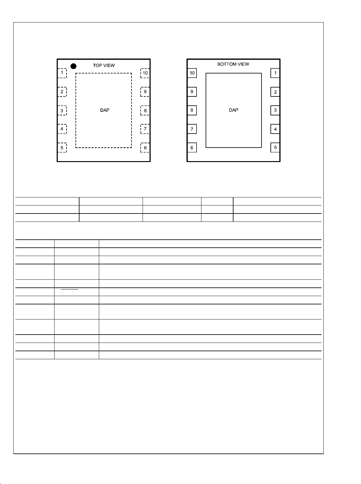
Connection Diagram
LM3509
Top View
10-Pin LLP (3mm × 3mm × 0.8mm)
30004302
Ordering Information
Order Number Package Type NSC Package Drawing Top Mark Supplied As
LM3509SD 10-Pin LLP SDA010A L3509 1000 units, Tape-and-Reel, No-Lead
LM3509SDX 10-Pin LLP SDA010A L3509 4500 units, Tape-and-Reel, No Lead
Pin Descriptions/Functions
Pin Name Function
1 MAIN Main Current Sink Input.
2 SUB/FB Secondary Current Sink Input or 1.25V Feedback Connection for Constant Voltage Output.
3 SET LED Current Setting Connection. Connect a resistor from SET to GND to set the maximum LED
current into MAIN or SUB/FB (when in LED mode), where I
4 VIO Logic Voltage Level Input
5 RESET/GPIO Active Low Hardware Reset and Programmable General Purpose I/O.
6 SW Drain Connection for Internal NMOS Switch
7 OVP Over-Voltage Protection Sense Connection. Connect OVP to the positive terminal of the output
capacitor.
8 IN Input Voltage Connection. Connect IN to the input supply, and bypass to GND with a 1µF ceramic
capacitor.
9 SDA Serial Data Input/Output
10 SCL Serial Clock Input
DAP GND Ground
LED_MAX
= 192×1.244V/R
SET
.
3 www.national.com

Absolute Maximum Ratings (Notes 1, 2)
If Military/Aerospace specified devices are required,
LM3509
please contact the National Semiconductor Sales Office/
Distributors for availability and specifications.
V
IN
VSW, V
V
SUB/FB
V
SCL
V
SET
Continuous Power Dissipation Internally Limited
Junction Temperature (T
Storage Temperature Range -65ºC to +150º C
, V
OVP
, V
SDA
,
MAIN
, V
RESET\GPIO
, VIO ,
J-MAX
−0.3V to 25V
−0.3V to 23V
)
−0.3V to 6V
−0.3V to 6V
+150ºC
Operating Ratings (Notes 1, 2)
V
IN
VSW, V
V
SUB/FB
OVP
, V
,
MAIN
Junction Temperature Range
(TJ)(Note 4)
Ambient Temperature Range
(TA)(Note 5)
Thermal Properties
Junction to Ambient Thermal
Resistance (θJA)(Note 6)
-40ºC to +110ºC
-40ºC to +85ºC
Maximum Lead Temperature
(Soldering, 10s)(Note 3) +300°C
ESD Rating(Note 10)
Human Body Model 2.5kV
ESD Caution Notice
National Semiconductor recommends that all integrated circuits be handled with appropriate ESD precautions. Failure to
observe proper ESD handling techniques can result in damage to the device.
Electrical Characteristics
Specifications in standard type face are for TA = 25°C and those in boldface type apply over the Operating Temperature Range
of TA = −40°C to +85°C. Unless otherwise specified VIN = 3.6V, VIO = 1.8V, V
RESET/GPIO
12.0kΩ, OLED = ‘0’, ENM = ENS = ‘1’, BSUB = BMAIN = Full Scale.(Notes 2, 7)
Symbol Parameter Conditions Min Typ Max Units
I
LED
I
LED-MATCH
Output Current Regulation
MAIN or SUB/FB Enabled
Maximum Current Per
Current Sink
I
MAIN
to I
SUB/FB
Current
UNI = ‘0’, or ‘1’
R
= 8.0kΩ
SET
UNI = ‘1’ (Note 11)
Matching
V
SET
I
LED/ISET
SET Pin Voltage 3.0V < VIN < 5V
I
Current to I
LED
SET
Current
Ratio
V
REG_CS
Regulated Current Sink
Headroom Voltage
V
REG_OLED
V
Regulation Voltage
SUB/FB
3.0V < VIN < 5.5V, OLED = ‘1’
in OLED Mode
V
HR
Current Sink Minimum
I
= 95% of nominal
LED
Headroom Voltage
R
DSON
NMOS Switch On
ISW = 100mA
Resistance
I
CL
V
OVP
f
SW
D
MAX
D
MIN
I
Q
NMOS Switch Current Limit VIN = 3.0V
Output Over-Voltage
Protection
ON Threshold 21.2 22 22.9
OFF Threshold 19.7 20.6 21.2
Switching Frequency
Maximum Duty Cycle
Minimum Duty Cycle
Quiescent Current, Device
Not Switching
V
MAIN
V
REG_CS
and V
, BSUB = BMAIN =
SUB/FB
>
0x00
V
SUB/FB
> V
REG_OLED
,
OLED=’1’, ENM=ENS=’0’
I
SHDN
Shutdown Current ENM = ENS = OLED = '0'
= VIN, V
18.6
= V
SUB/FB
= 0.5V, R
MAIN
20 21.8
30
0.15 1 %
1.244 V
192
500 mV
1.172 1.21 1.239 V
300 mV
0.58
650 770 875 A
1.0 1.27 1.4 MHz
90 %
10 %
400 440
250 305
3.6 5 µA
2.7V to 5.5V
0V to 23V
0V to 21V
54°C/W
=
SET
mA
Ω
V
µA
www.national.com 4
Symbol Parameter Conditions Min Typ Max Units
RESET/GPIO Pin Voltage Specifications
V
IL
V
IH
V
OL
Input Logic Low 2.7V < VIN <5.5V, MODE bit
= 0
Input Logic High 2.7V < VIN < 5.5V, MODE bit
= 0
Output Logic Low I
=3mA, MODE bit = 1
LOAD
0.5 V
1.1 V
400 mV
I2C Compatible Voltage Specifications (SCL, SDA, VIO)
V
IO
V
IL
V
IH
V
OL
Serial Bus Voltage Level 2.7V < VIN < 5.5V (Note 9)
Input Logic Low 2.7V < VIN < 5.5V
Input Logic High 2.7V < VIN < 5.5V
Output Logic Low I
LOAD
= 3mA
1.4
0.7×V
IO
V
IN
0.36×V
V
IO
IO
400 mV
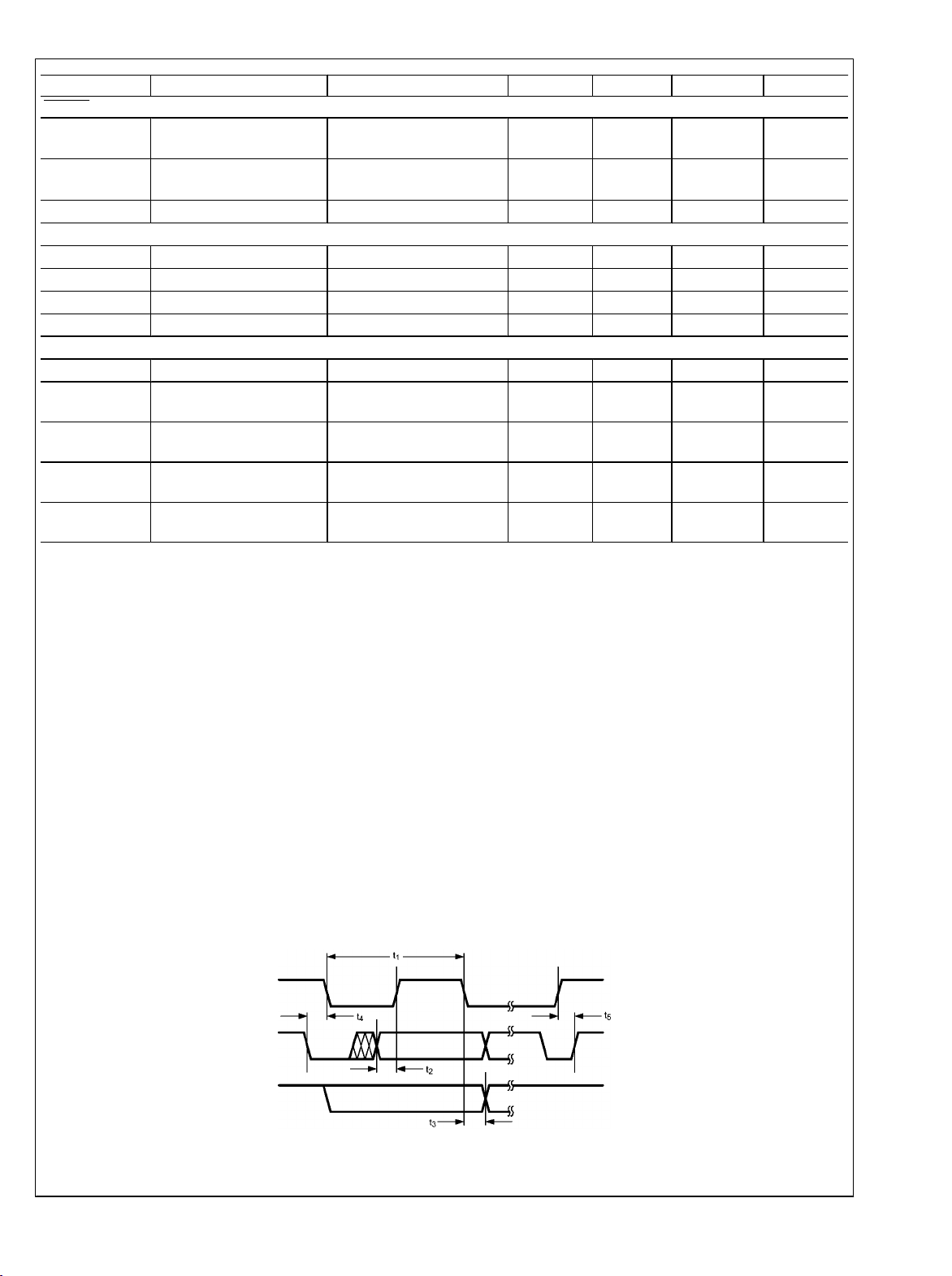
I2C Compatible Timing Specifications (SCL, SDA, VIO, see Figure 1) (Notes 8, 9)
t
1
t
2
t
3
t
4
t
5
SCL Clock Period
Data In Setup Time to SCL
High
Data Out Stable After SCL
Low
SDA Low Setup Time to
SCL Low (Start)
SDA High Hold Time After
SCL High (Stop)
2.5 µs
100 ns
0 ns
100 ns
100 ns
LM3509
V
V
V
Note 1: Absolute maximum ratings are limits beyond which damage to the device may occur. Operating Ratings are conditions for which the device is intended
to be functional, but device parameter specifications may not be guaranteed. For guaranteed specifications and test conditions, see the Electrical Characteristics.
Note 2: All voltages are with respect to the potential at the GND pin.
Note 3: For detailed soldering specifications and information, please refer to National Semiconductor Application Note 1187: Leadless Lead frame Package
(AN-1187).
Note 4: Internal thermal shutdown circuitry protects the device from permanent damage. Thermal shutdown engages at TJ=150ºC (typ.) and disengages at
TJ=140ºC (typ.).
Note 5: In applications where high power dissipation and/or poor package thermal resistance is present, the maximum ambient temperature may have to be
derated. Maximum ambient temperature (T
dissipation of the device in the application (P
following equation: T
Note 6: Junction-to-ambient thermal resistance (θJA) is taken from a thermal modeling result, performed under the conditions and guidelines set forth in the
JEDEC standard JESD51-7. The test board is a 4-layer FR-4 board measuring 114mm x 76mm x 1.6mm with a 2x1 array of thermal vias. The ground plane on
the board is 113mm x 75mm. Thickness of copper layers are 71.5µm/35µm/35µm/71.5µm (2oz/1oz/1oz/2oz). Ambient temperature in simulation is 22°C, still air.
Power dissipation is 1W. The value of θJA of this product in the LLP package could fall in a range as wide as 50ºC/W to 150ºC/W (if not wider), depending on
board material, layout, and environmental conditions. In applications where high maximum power dissipation exists special care must be paid to thermal dissipation
issues. For more information on these topics, please refer to Application Note 1187: Leadless Leadframe Package (LLP) and the Power Efficiency and Power
Dissipation section of this datasheet.
Note 7: Min and Max limits are guaranteed by design, test, or statistical analysis. Typical (Typ) numbers are not guaranteed, but represent the most likely norm.
Note 8: SCL and SDA must be glitch-free in order for proper brightness control to be realized.
Note 9: SCL and SDA signals are referenced to VIO and GND for minimum VIO voltage testing.
Note 10: The human body model is a 100pF capacitor discharged through 1.5kΩ resistor into each pin. (MIL-STD-883 3015.7).
Note 11: The matching specification between MAIN and SUB is calculated as 100 × ((I
100 × (I
MAIN
- I
SUB
)/(I
A-MAX
MAIN
+ I
= T
J-MAX-OP
SUB
– (θJA × P
).
) is dependent on the maximum operating junction temperature (TJ-MAX-OP = +105ºC), the maximum power
A-MAX
), and the junction-to ambient thermal resistance of the part/package in the application (θJA), as given by the
D-MAX
).
D-MAX
or I
) - I
) / I
MAIN
SUB
. This simplifies out to be
AVE
AVE
FIGURE 1. I2C Timing
5 www.national.com
30004303

Typical Performance Characteristics V
Mode), C
LM3509
I
SUB
+ I
= 2.2µF (OLED Mode), CIN = 1µF, L = TDK VLF4012AT-100MR79, (RL = 0.3Ω), R
OUT
, TA = +25°C unless otherwise specified.
MAIN
= 3.6V, LEDs are OSRAM (LW M67C), C
IN
= 8.06kΩ, UNI = '1', I
SET
= 1µF (LED
OUT
LED
=
10 LED Efficiency vs I
(2 Strings of 5LEDs)
6 LED Efficiency vs I
(2 Strings of 3LEDs)
LED
LED
30004308
8 LED Efficiency vs I
(2 Strings of 4LEDs)
4 LED Efficiency vs I
(2 Strings of 2LEDs)
LED
30004309
LED
30004310
LED Efficiency vs V
(L = TDK VLF3012AT-100MR49, RL = 0.36Ω, I
www.national.com 6
IN
LED
30004357
= 40mA)
LED Efficiency vs V
IN
(L = TDK VLF5014AT-100MR92, RL = 0.2Ω, I
30004311
LED
30004358
= 60mA)

LM3509
18V OLED Efficiency vs I
LED Line Regulation
(UNI = '0')
OUT
30004304
12V OLED Efficiency vs I
OLED Line Regulation
I
= 60mA
OLED
OUT
30004305
OLED Line Regulation
I
= 60mA
OLED
30004359
30004306
OLED Load Regulation
V
= 18V
OLED
30004307
30004313
7 www.national.com

LM3509
OLED Load Regulation
V
= 12V
OLED
Peak Current Limit vs. V
IN
Over Voltage Limit vs. V
Switching Frequency vs. V
IN
30004312
30004315
IN
Switch On-Resistance vs. V
Maximum Duty Cycle vs. V
30004314
IN
30004317
IN
30004318
www.national.com 8
30004319

LM3509
Shutdown Current vs. V
IN
30004320
LED Current Matching vs. CODE (Note 11)
(UNI = '1', R
= 12kΩ, TA = -40°C to +85°C)
SET
Switching Supply Current vs. V
LED Current Accuracy vs CODE
(R
= 12kΩ±0.05%)
SET
IN
30004321
(I
LED Current vs CODE
, I
SUB
, I
IDEAL
MAIN
, R
= 12kΩ±0.05%)
SET
30004322
30004324
I
vs Current Source Headroom Voltage
LED
(VIN = 3V, UNI = '0')
30004323
30004360
9 www.national.com

LM3509
Start-Up Waveform (LED Mode)
(2 × 5 LEDs, 30mA per string)
Start-Up Waveform (OLED Mode)
(V
OUT
= 18V, I
= 60mA)
OUT
Channel 1: SDA (5V/div)
Channel 2: V
Channel 3: I
(10V/div)
OUT
(50mA/div)
LED
Channel 4: IIN (500mA/div)
Time Base: 400µs/div
Load Step (OLED Mode)
(V
Channel 1: V
Channel 2: I
Time Base: 200µs/div
(AC Coupled, 500mV/div)
OUT
(20mA/div)
OUT
Transition From OLED to OLED + 1 × 4 LED)
(V
= 18V, I
OUT
OUT
= 18V, C
OUT
= 40mA, I
= 2.2µF)
OUT
= 20mA, C
LED
30004325
OUT
30004326
= 2.2µF)
Channel 1: SDA (5V/div)
Channel 2: V
Channel 3: I
(10V/div)
OUT
(50mA/div)
OUT
Channel 4: IIN (500mA/div)
Time Base: 400µs/div
Line Step (LED Mode)
(2 × 5 LEDs, 30mA per String, C
Channel 1: V
Channel 2: VIN (AC Coupled, 500mV/div)
Time Base: 200µs/div
(AC Coupled, 500mV/div)
OUT
RESET Functionality
30004327
OUT
= 1µF)
30004354
Channel 3: SDA (2V/div)
30004328
Channel 1: V
Channel 2: I
(AC Coupled, 200mV/div)
OUT
(20mA/div)
MAIN
Time Base: 400µs/div
www.national.com 10
Channel 2: I
Channel R1: I
(20mA/div)
SUB
MAIN
(20mA/div)
Channel 1: RESET (2V/div)
Time Base: 200ns/div
30004352

LM3509
(GPIO Configured as OUTPUT, f
GPIO Functionality
Channel 2: GPIO (2V/div)
Channel 3: SDA (2V/div)
Channel 1:SCL (2V/div)
Time Base: 40µs/div
Ramp Rate Functionality
(RMP1, RMP0 = '01')
= 200kHz)
SCL
30004353
Channel 3: SDA (2V/div)
Channel 1: I
Channel 4: I
(10mA/div)
MAIN
(10mA/div)
SUB
Time Base: 40µs/div
Ramp Rate Functionality
(RMP1, RMP0 = '00')
30004330
Ramp Rate Functionality
(RMP1, RMP0 = '10')
Channel 3: SDA (2V/div)
Channel 1: I
Channel 4: I
(10mA/div)
MAIN
(10mA/div)
SUB
Time Base: 100ms/div
Channel 1:I
Channel 4: I
(10mA/div)
MAIN
(10mA/div)
SUB
Time Base: 400ms/div
Ramp Rate Functionality
(RMP1, RMP0 = '11')
30004355
30004351
Channel 1:I
Channel 4: I
(10mA/div)
MAIN
(10mA/div)
SUB
Time Base: 200ms/div
30004356
11 www.national.com

Block Diagram
LM3509
FIGURE 2. LM3509 Block Diagram
Operation Description
The LM3509 Current Mode PWM boost converter operates
from a 2.7V to 5.5V input and provides two regulated outputs
for White LED and OLED display biasing. The first output,
MAIN, provides a constant current of up to 30mA to bias up
to 5 series white LED’s. The second output, SUB/FB, can be
configured as a current source for up to 5 series white LED’s
at at 30mA, or as a feedback voltage pin to regulate a constant
output voltage of up to 21V. When both MAIN and SUB/FB
are configured for white LED bias the current for each LED
string is controlled independently or in unison via an I2C compatible interface. When MAIN is configured for white LED bias
and SUB/FB is configured as a feedback voltage pin, the current into MAIN is controlled via the I2C compatible interface
and SUB/FB becomes the middle tap of a resistive divider
used to regulate the output voltage of the boost converter.
The core of the LM3509 is a Current Mode Boost converter.
Operation is as follows. At the start of each switching cycle
the internal oscillator sets the PWM converter. The converter
turns the NMOS switch on, allowing the inductor current to
www.national.com 12
30004333
ramp while the output capacitor supplies power to the white
LED’s and/or OLED panel. The error signal at the output of
the error amplifier is compared against the sensed inductor
current. When the sensed inductor current equals the error
signal, or when the maximum duty cycle is reached, the
NMOS switch turns off causing the external Schottky diode to
pick up the inductor current. This allows the inductor current
to ramp down causing its stored energy to charge the output
capacitor and supply power to the load. At the end of the clock
period the PWM controller is again set and the process repeats itself.
ADAPTIVE REGULATION
When biasing dual white led strings (White LED mode) the
LM3509 maximizes efficiency by adaptively regulating the
output voltage. In this configuration the 500mV reference is
connected to the non-inverting input of the error amplifier via
mux S2 (see Figure 2, Block Diagram). The lowest of either
V
or V
MAIN
error amplifier via mux S1. This ensures that V
are at least 500mV, thus providing enough voltage head-
FB
is then applied to the inverting input of the
SUB/FB
MAIN
and V
SUB/

LM3509
room at the input to the current sinks for proper current
regulation.
In the instance when there are unequal numbers of LEDs or
unequal currents from string to string, the string with the highest voltage will be the regulation point.
UNISON/NON-UNISON MODE
Within White LED mode there are two separate modes of operation, Unison and Non-Unison. Non-Unison mode provides
for independent current regulation, while Unison mode gives
up independent regulation for more accurate matching between LED strings. When in Non-Unison mode the LED currents I
registers BMAIN and BSUB respectively (see Brightness
MAIN
and I
are independently controlled via
SUB/FB
Registers (BMAIN and BSUB) section). When in Unison
mode BSUB is disabled and both I
trolled via BMAIN only.
MAIN
and I
SUB/FB
are con-
START-UP
The LM3509 features an internal soft-start, preventing large
inrush currents during start-up that can cause excessive voltage ripple on the input. For the typical application circuits
when the device is brought out of shutdown the average input
current ramps from zero to 450mA in 1.2ms. See Start Up
Plots in the Typical Performance Characteristics.
OLED MODE
When the LM3509 is configured for a single White LED bias
+ OLED display bias (OLED mode), the non-inverting input of
the error amplifier is connected to the internal 1.21V reference
via MUX S2. MUX S1 switches SUB/FB to the inverting input
of the error amplifier while disconnecting the internal current
sink at SUB/FB. The voltage at MAIN is not regulated in OLED
mode so when the application requires white LED + OLED
panel biasing, ensure that at least 300mV of headroom is
maintained at MAIN to guarantee proper regulation of I
(see the Typical Performance Characteristics for a plot of
I
vs Current Source Headroom Voltage)
LED
MAIN
PEAK CURRENT LIMIT
The LM3509’s boost converter has a peak current limit for the
internal power switch of 770mA typical (650mA minimum).
When the peak switch current reaches the current limit the
duty cycle is terminated resulting in a limit on the maximum
output current and thus the maximum output power the
LM3509 can deliver. Calculate the maximum LED current as
a function of VIN, V
OUT
, L and I
PEAK
as:
21.2V. In White LED mode during output open circuit conditions the output voltage will rise to the over voltage protection
threshold (V
troller will stop switching causing V
output voltage drops below 19.7V (min) the device will resume
= 21.2V min). When this happens the con-
OVP
to droop. When the
OUT
switching. If the device remains in an over voltage condition
the LM3509 will repeat the cycle causing the output to cycle
between the high and low OVP thresholds. See waveform for
OVP condition in the Typical Performance Characteristics.
OUTPUT CURRENT ACCURACY AND CURRENT MATCHING
The LM3509 provides both precise current accuracy (% error
from ideal value) and accurate current matching between the
MAIN and SUB/FB current sinks. Two modes of operation affect the current matching between I
mode (Non-Unison mode) is set by writing a 0 to bit 2 of the
MAIN
and I
SUB/FB
. The first
General Purpose register (UNI bit). Non-Unison mode allows
for independent programming of I
BMAIN and BSUB respectively. In this mode typical matching
MAIN
and I
SUB/FB
via registers
between current sinks is 1%.
Writing a 1 to UNI configures the device for Unison mode. In
Unison mode, BSUB is disabled and I
controlled via register BMAIN. In this mode typical matching
MAIN
and I
SUB/FB
are both
is 0.15%.
LIGHT LOAD OPERATION
The LM3509 boost converter operates in three modes; continuous conduction, discontinuous conduction, and skip mode
operation. Under heavy loads when the inductor current does
not reach zero before the end of the switching period the device switches at a constant frequency. As the output current
decreases and the inductor current reaches zero before the
end of the switching cycle, the device operates in discontinuous conduction. At very light loads the LM3509 will enter skip
.
mode operation causing the switching period to lengthen and
the device to only switch as required to maintain regulation at
the output.
ACTIVE LOW RESET/GENERAL PURPOSE I/O (RESET \GPIO)
The RESET/GPIO serves as an active low reset input or as a
general-purpose logic input/output. Upon power-up of the device RESET/GPIO defaults to the active low reset mode. The
functionality of RESET/GPIO is set via the GPIO register and
is detailed in Table 6. When configured as an active low reset
input, (Bit 0 = 0), pulling RESET/GPIO low automatically programs all registers of the LM3509 with 0x00. Their state
cannot be changed until RESET/GPIO is pulled high. The
General Purpose I/O (GPIO) register is used to enable the
GPIO function of the RESET/GPIO pin. The GPIO register is
an 8-bit register with only the 3 LSB’s active. The 5 MSB’s are
not used. When configured as an output, RESET/GPIO is
open drain and requires an external pull-up resistor.
ƒSW = 1.27MHz. Typical values for efficiency and I
be found in the efficiency and I
formance Characteristics.
curves in the Typical Per-
PEAK
OVER VOLTAGE PROTECTION
The LM3509's output voltage (V
by the Output Over-Voltage Protection Threshold (V
) is limited on the high end
OUT
PEAK
OVP
THERMAL SHUTDOWN
The LM3509 offers a thermal shutdown protection. When the
can
die temperature reaches +140°C the device will shutdown
and not turn on again until the die temperature falls below
+120°C.
) of
13 www.national.com

I2C COMPATIBLE INTERFACE
The LM3509 is controlled via an I2C compatible interface.
LM3509
START and STOP conditions classify the beginning and the
end of the I2C session. A START condition is defined as SDA
transitioning from HIGH to LOW while SCL is HIGH. A STOP
condition is defined as SDA transitioning from LOW to HIGH
while SCL is HIGH. The I2C master always generates START
and STOP conditions. The I2C bus is considered busy after a
FIGURE 3. Start and Stop Sequences
START condition and free after a STOP condition. During data transmission, the I2C master can generate repeated
START conditions. A START and a repeated START conditions are equivalent function-wise. The data on SDA must be
stable during the HIGH period of the clock signal (SCL). In
other words, the state of SDA can only be changed when SCL
is LOW.
30004337
I2C COMPATIBLE ADDRESS
The chip address for the LM3509 is 0110110 (36h). After the
START condition, the I2C master sends the 7-bit chip address
followed by a read or write bit (R/W). R/W= 0 indicates a
FIGURE 4. Chip Address
TRANSFERRING DATA
Every byte on the SDA line must be eight bits long, with the
most significant bit (MSB) transferred first. Each byte of data
must be followed by an acknowledge bit (ACK). The acknowledge related clock pulse (9th clock pulse) is generated by the
master. The master releases SDA (HIGH) during the 9th clock
WRITE and R/W = 1 indicates a READ. The second byte following the chip address selects the register address to which
the data will be written. The third byte contains the data for
the selected register.
30004338
pulse. The LM3509 pulls down SDA during the 9th clock
pulse, signifying an acknowledge. An acknowledge is generated after each byte has been received. Figure 5 is an example of a write sequence to the General Purpose register of the
LM3509.
FIGURE 5. Write Sequence to the LM3509
www.national.com 14
30004339

REGISTER DESCRIPTIONS
There are 4, 8 bit registers within the LM3509 as detailed in Table 1.
TABLE 1. LM3509 Register Descriptions
Register Name Hex Address Power -On-Value
General Purpose (GP) 10 0xC0
Brightness Main (BMAIN) A0 0xE0
Brightness Sub (BSUB) B0 0xE0
General Purpose
I/O (GPIO)
80 0XF8
LM3509
GENERAL PURPOSE REGISTER (GP)
The General Purpose register has four functions. It controls
the on/off state of MAIN and SUB/FB, it selects between Unison or Non-Unison mode, provides for control over the rate of
change of the LED current (see Brightness Rate of Change
Description), and selects between White LED and OLED
mode. Figure 6 and Table 2 describes each bit available within the General Purpose Register.
30004340
FIGURE 6. General Purpose Register Description
TABLE 2. General Purpose Register Bit Function
Bit Name Function Power-On-Value
0 ENM Enable MAIN. Writing a 1 to this bit enables the main current sink (MAIN).
Writing a 0 to this bit disables the main current sink and forces MAIN high
impedance.
1 ENS Enable SUB/FB. Writing a 1 to this bit enables the secondary current sink (SUB/
FB). Writing a 0 to this bit disables the secondary current sink and forces SUB/
FB high impedance.
2 UNI Unison Mode Select. Writing a 1 to this bit disables the BSUB register and
causes the contents of BMAIN to set the current in both the MAIN and SUB/
FB current sinks. Writing a 0 to this bit allows the current into MAIN and SUB/
FB to be independently controlled via the BMAIN and BSUB registers
respectively.
3 RMP0 Brightness Rate of Change. Bits RMP0 and RMP1 set the rate of change of
4 RMP1 0
the LED current into MAIN and SUB/FB in response to changes in the contents
of registers BMAIN and BSUB (see brightness rate of change description).
5 OLED OLED = 0 places the LM3509 in White LED mode. In this mode both the MAIN
and SUB/FB current sinks are active. The boost converter ensures there is at
least 500mV at V
MAIN
and V
SUB/FB
.
OLED = 1 places the LM3509 in OLED mode. In this mode the boost converter
regulates V
SUB/FB
to 1.25V. V
is unregulated and must be > 400mV for the
MAIN
MAIN current sink to maintain current regulation.
6 Don't Care These are non-functional read only bits. They will always read back as a 1. 1
7
0
0
0
0
0
15 www.national.com

TABLE 3. Operational Truth Table
LM3509
UNI OLED ENM ENS Result
X 0 0 0 LM3509 Disabled
1 0 1 X MAIN and SUB/FB current sinks enabled. Current levels set by
1 0 0 X MAIN and SUB/FB Disabled
0 0 0 1 SUB/FB current sink enabled. Current level set by BSUB.
0 0 1 0 MAIN current sink enabled. Current level set by BMAIN.
0 0 1 1 MAIN and SUB/FB current sinks enabled. Current levels set by
X 1 1 X SUB/FB current sink disabled (SUB/FB configured as a feedback
X 1 0 X SUB/FB current sink disabled (SUB/FB configured as a feedback
contents of BMAIN.
contents of BMAIN and BSUB respectively.
pin). MAIN current sink enabled current level set by BMAIN.
pin). MAIN current sink disabled.
* ENM ,ENS, or OLED high enables analog circuitry.
BRIGHTNESS REGISTERS (BMAIN and BSUB)
With the UNI bit (General Purpose register) set to 0 (NonUnison mode) both brightness registers (BMAIN and BSUB)
independently control the LED currents I
spectively. BMAIN and BSUB are both 8 bit, but with only the
MAIN
and I
SUB/FB
re-
5 LSB’s controlling the current. The three MSB’s are don’t
cares. The LED current control is designed to approximate an
exponentially increasing response of the LED current vs increasing code in either BMAIN or BSUB (see Figure 9).
Program I
to GND, where:
by connecting a resistor (RSET) from SET
LED_MAX
FIGURE 7. Brightness MAIN Register Description
. With the UNI bit (General Purpose register) set to 1 (Unison
mode), BSUB is disabled and BMAIN sets both I
. This prevents the independent control of I
FB
, however matching between current sinks goes from typi-
FB
cally 1%(with UNI = 0) to typically 0.15% (with UNI = 1). Figure
MAIN
MAIN
and I
and I
SUB/
SUB/
7 and Figure 8 show the register descriptions for the Brightness MAIN and Brightness SUB registers. Table 4 and Figure
9 show I
age of I
and/or I
MAIN
LED_MAX
vs. brightness data as a percent-
SUB/FB
.
30004342
FIGURE 8. Brightness SUB Register Description
www.national.com 16
30004343

LM3509
TABLE 4. I
BMAIN or BSUB Brightness
00000 0.000% 10000 8.750%
00001 0.125% 10001 10.000%
00010 0.625% 10010 12.500%
00011 1.000% 10011 15.000%
00100 1.125% 10100 16.875%
00101 1.313% 10101 18.750%
00110 1.688% 10110 22.500%
00111 2.063% 10111 26.250%
01000 2.438% 11000 31.250%
01001 2.813% 11001 37.500%
01010 3.125% 11010 43.750%
01011 3.750% 11011 52.500%
01100 4.375% 11100 61.250%
01101 5.250% 11101 70.000%
01110 6.250% 11110 87.500%
01111 7.500% 11111 100.000%
vs. Brightness Register Data
LED
Data
% of ILED_MAX BMAIN or BSUB Brightness Data % of ILED_MAX
FIGURE 9. I
MAIN
30004344
or I
vs BMAIN or BSUB Data
SUB
17 www.national.com

BRIGHTNESS RATE OF CHANGE DESCRIPTION
RMP0 and RMP1 control the rate of change of the LED cur-
LM3509
rent I
or BSUB. There are 4 user programmable LED current rates
MAIN
and I
in response to changes in BMAIN and /
SUB/FB
of change settings for the LM3509 (see Table 5).
TABLE 5. Rate of Change Bits
RMP0 RMP1 Change Rate
(t
STEP
0 0 51µs/step
0 1 13ms/step
1 0 26ms/step
1 1 52ms/step
For example, if R
contents of BMAIN set to 0x1F (I
contents of BMAIN are changed to 0x00 resulting in (I
0mA). With RMP0 =1 and RMP1 = 1 (52ms/step), I
change from 20mA to 0mA in 31 steps with 52ms elapsing
between steps, excluding the step from 0x1F to 0x1E, resulting in a full scale current change in 1560ms. The total time to
transition from one brightness code to another is:
The following 3 additional examples detail possible scenarios
when using the brightness register in conjunction with the rate
of change bits and the enable bits.
Example 1:
Step 1: Write to BMAIN a value corresponding to I
mA.
= 12kΩ then I
SET
= 20mA. With the
LED_MAX
= 20mA), suppose the
MAIN
Step 2: Write 1 to ENM (turning on MAIN)
Step 3: I
RMP1. (RMP0 and RMP1 bits set the duration spent at one
ramps to 20mA with a rate set by RMP0 and
MAIN
brightness code before incrementing to the next).
Step 4: ENM is set to 0 before 20mA is reached, thus the LED
current fades off at a rate given by RMP0 and RMP1 without
I
going up to 20mA.
MAIN
Example 2:
)
Step 1: ENM is 1, and BMAIN has been programmed with
code 0x01. This results in a small current into MAIN.
Step 2: BMAIN is programmed with 0x1F (full scale current).
MAIN
MAIN
will
This causes I
ed by RMP0 and RMP1.
Step 3: Before I
with 0x09. I
Step 4: When I
=
down to the current corresponding to 0x09 at a rate set by
RMP0 and RMP1.
to ramp toward full-scale at the rate select-
MAIN
reaches full-scale BMAIN is programmed
MAIN
will continue to ramp to full scale.
MAIN
has reached full-scale value it will ramp
MAIN
Example 3:
Step 1: Write to BMAIN a value corresponding to I
mA.
MAIN
= 20-
Step 2: Write a 1 to both RMP0 and RMP1.
Step 3: Write 1 to ENM (turning on MAIN).
Step 4: I
RMP1. (RMP0 and RMP1 bits set the duration spent at one
ramps toward 20mA with a rate set by RMP0 and
MAIN
brightness code before incrementing to the next).
Step 5: After 1.04s I
(0.16875 × 20mA = 3.375mA). Simultaneously, RMP0 and
has ramped to 16.875% of I
MAIN
LED_MAX
RMP1 are both programmed with 0.
MAIN
= 20-
Step 6: I
at a new ramp rate of 51µs/step.
continues ramping from 3.375mA to 20mA, but
MAIN
TABLE 6. GPIO Register Function
Bits 7 – 3 Data (Bit 2) Mode (Bit 1) Enable GPIO (Bit 0) Function
X X X 0 RESET/GPIO is configured as an active low reset
input. This is the default power on state.
X Logic Input 0 1 RESET/GPIO is configured as a logic input. The logic
level applied to RESET/GPIO can be read via bit 2 of
the GPIO register.
X Logic Output 1 1 RESET/GPIO is configured as a logic output. A 0 in
bit 2 forces RESET/GPIO low. A 1 in bit 2 forces
RESET/GPIO high impedance.
30004346
FIGURE 10. GPIO Register Description
SHUTDOWN AND OUTPUT ISOLATION
The LM3509 provides a true shutdown for either MAIN or
SUB/FB when configured as a White LED bias supply. Write
a 0 to ENM (bit 1) of the General Purpose register to turn off
the MAIN current sink and force MAIN high impedance. Write
a 0 to ENS (bit 2) of the General Purpose register to turn off
the SUB/FB current sink and force SUB/FB high impedance.
Writing a 1 to ENM or ENS turns on the MAIN and SUB/FB
current sinks respectively. When in shutdown the leakage
current into MAIN or SUB/FB is typically 3.6µA. See Typical
Performance Plots for start-up responses of the LM3509 using the ENM and ENS bits in White LED and OLED modes.
www.national.com 18

LM3509
Application Information
LED CURRENT SETTING/MAXIMUM LED CURRENT
Connect a resistor (R
maximum LED current (I
R
SET
to I
LED_MAX
relationship is:
where SET provides the constant 1.244V output.
OUTPUT VOLTAGE SETTING (OLED MODE)
Connect Feedback resistors from the converters output to
SUB/FB to GND to set the output voltage in OLED mode (see
R1 and R2 in the Typical Application Circuit (OLED Panel
Power Supply). First select R2 < 100kΩ then calculate R1
such that:
In OLED mode the MAIN current sink continues to regulate
the current through MAIN, however, V
lated. To avoid dropout and ensure proper current regulation
the application must ensure that V
OUTPUT CAPACITOR SELECTION
The LM3509’s output capacitor supplies the LED current during the boost converters on time. When the switch turns off
the inductor energy is discharged through the diode supplying
power to the LED’s and restoring charge to the output capacitor. This causes a sag in the output voltage during the on time
and a rise in the output voltage during the off time. The output
capacitor is therefore chosen to limit the output ripple to an
acceptable level depending on LED or OLED panel current
requirements and input/output voltage differentials. For proper operation ceramic output capacitors ranging from 1µF to
2.2µF are required.
As with the input capacitor, the output voltage ripple is com-
posed of two parts, the ripple due to capacitor discharge (delta
VQ) and the ripple due to the capacitors ESR (delta V
continuous conduction mode, the ripple components are
found by:
) from SET to GND to program the
SET
) into MAIN or SUB/FB. The
LED_MAX
is no longer regu-
MAIN
> 0.3V.
MAIN
ESR
). For
INPUT CAPACITOR SELECTION
Choosing the correct size and type of input capacitor helps
minimize the input voltage ripple caused by the switching of
the LM3509’s boost converter. For continuous inductor current operation the input voltage ripple is composed of 2 primary components, the capacitor discharge (delta VQ) and the
capacitor’s equivalent series resistance (delta V
ripple components are found by:
ESR
). These
In the typical application circuit a 1µF ceramic input capacitor
works well. Since the ESR in ceramic capacitors is typically
less than 5mΩ and the capacitance value is usually small, the
input voltage ripple is primarily due to the capacitive discharge. With larger value capacitors such as tantalum or
aluminum electrolytic the ESR can be greater than 0.5Ω. In
this case the input ripple will primarily be due to the ESR.
Table 7 lists different manufacturers for various capacitors
and their case sizes that are suitable for use with the LM3509.
When configured as a dual output LED driver a 1µF output
capacitor is adequate. In OLED mode for output voltages
above 12V a 2.2µF output capacitor is required (see Low
Output Voltage Operation (OLED) Section).
19 www.national.com

TABLE 7. Recommended Output Capacitors
LM3509
Manufacturer Part Number Value Case Size Voltage Rating
TDK C1608X5R1E105M 1µF 0603 25V
Murata GRM39X5R105K25D53
9
TDK C2012X5R1E225M 2.2µF 0805 25V
Murata GRM219R61E225KA12 2.2µF 0805 25V
INDUCTOR SELECTION
The LM3509 is designed for use with a 10µH inductor, however 22µH are suitable providing the output capacitor is increased 2×'s. When selecting the inductor ensure that the
saturation current rating (I
enough and the inductor is large enough such that at the
maximum LED current the peak inductor current is less than
the LM3509’s peak switch current limit. This is done by choosing:
) for the chosen inductor is high
SAT
1µF 0603 25V
Values for I
vs. VIN in the Typical Performance Characteristics graphs.
Table 8 shows possible inductors, as well as their corresponding case size and their saturation current ratings.
can be found in the plot of peak current limit
PEAK
TABLE 8. Recommended Inductors
Manufacturer Part Number Value Dimensions I
TDK VLF3012AT-100M
R49
TDK VLF4012AT-100M
R79
TOKO A997AS-100M 10µH 3.8mm×3.8mm×1.
DIODE SELECTION
The output diode must have a reverse breakdown voltage
greater than the maximum output voltage. The diodes average current rating should be high enough to handle the
LM3509’s output current. Additionally, the diodes peak current rating must be high enough to handle the peak inductor
current. Schottky diodes are recommended due to their lower
10µH 2.6mm×2.8mm×1
mm
10µH 3.5mm×3.7mm×1.
2mm
8mm
forward voltage drop (0.3V to 0.5V) compared to (0.6V to
0.8V) for PN junction diodes. If a PN junction diode is used,
ensure it is the ultra-fast type (trr < 50ns) to prevent excessive
loss in the rectifier. For Schottky diodes the B05030WS (or
equivalent) work well for most designs. See Table 9 for a list
of other Schottky Diodes with similar performance.
SAT
490mA
800mA
580mA
TABLE 9. Recommended Schottky Diodes
Manufacturer Part Number Package Reverse Breakdown
Voltage
Diodes Inc. B05030WS SOD-323 30V 0.5A
Philips BAT760 SOD-323 23V 1A
ON Semiconductor NSR0320MW2T SOD-323 30V 1A
Average Current Rating
DC Resistance
0.36Ω
0.3Ω
0.18Ω
www.national.com 20

LM3509
OUTPUT CURRENT RANGE (OLED MODE)
The maximum output current the LM3509 can deliver in OLED
mode is limited by 4 factors (assuming continuous conduction); the peak current limit of 770mA (typical), the inductor
value, the input voltage, and the output voltage. Calculate the
maximum output current (I
tion:
For the typical application circuit with V
ing 70% efficiency, the maximum output current at VIN = 2.7V
) using the following equa-
OUT_MAX
= 18V and assum-
OUT
will be approximately 70mA. At 4.2V due to the shorter on
times and lower average input currents the maximum output
current (at 70% efficiency) jumps to approximately 105mA.
Figure 11 shows a plot of I
equation, assuming 80% efficiency. In reality factors such as
vs. VIN using the above
OUT_MAX
current limit and efficiency will vary over VIN, temperature, and
component selection. This can cause the actual I
be higher or lower.
30004362
OUT_MAX
to
FIGURE 11. Typical Maximum Output Current in OLED
Mode
OUTPUT VOLTAGE RANGE (OLED MODE)
The LM3509's output voltage is constrained by 2 factors. On
the low end it is limited by the minimum duty cycle of 10%
(assuming continuous conduction) and on the high end it is
limited by the over voltage protection threshold (V
(typical). In order to maintain stability when operating at dif-
OVP
) of 22V
ferent output voltages the output capacitor and inductor must
be changed. Refer to Table 10 for different V
L combinations.
OUT
, C
OUT
, and
TABLE 10. Component Values for Output Voltage Selection
V
OUT
18V
15V
12V
9V
7V
5V
LAYOUT CONSIDERATIONS
The LLP is a leadless package with very good thermal properties. This package has an exposed DAP (die attach pad) at
the underside center of the package measuring 1.6mm x
2.0mm. The main advantage of this exposed DAP is to offer
low thermal resistance when soldered to the thermal ground
pad on the PCB. For good PCB layout a 1:1 ratio between the
package and the PCB thermal land is recommended. To further enhance thermal conductivity, the PCB thermal ground
pad may include vias to a 2nd layer ground plane. For more
detailed instructions on mounting LLP packages, please refer
to National Semiconductor Application Note AN-1187.
The high switching frequencies and large peak currents make
the PCB layout a critical part of the design. The proceeding
steps must be followed to ensure stable operation and proper
current source regulation.
1, Divide ground into two planes, one for the return terminals
of C
, CIN and the I2C Bus, the other for the return terminals
OUT
of R
and the feedback network. Connect both planes to the
SET
exposed PAD, but nowhere else.
2, Connect the inductor and the anode of D1 as close together
as possible and place this connection as close as possible to
the SW pin. This reduces the inductance and resistance of
the switching node which minimizes ringing and excess voltage drops. This will improve efficiency and decrease noise
that can get injected into the current sources.
3, Connect the return terminals of the input capacitor and the
output capacitor as close as possible to the exposed PAD and
through low impedance traces.
4, Bypass IN with at least a 1µF ceramic capacitor. Connect
the positive terminal of this capacitor as close as possible to
IN.
5, Connect C
This reduces the inductance and resistance of the output bypass node which minimizes ringing and the excess voltage
drops. This will improving efficiency and decrease noise that
can get injected into the current sources.
6, Route the traces for R
from the SW node to minimize noise injection.
7, Do not connect any external capacitance to the SET pin.
C
OUT
L VIN Range
2.2µF 10µH 2.7V to
2.2µF 10µH 2.7V to
4.7µF 10µH 2.7V to
10µF 10µH 2.7V to
10µF 4.7µH 2.7V to
22µF 4.7µH 2.7V to
as close as possible to the cathode of D1.
OUT
and the feedback divider away
SET
5.5V
5.5V
5.5V
5.5V
5.5V
4.5V
21 www.national.com

Physical Dimensions inches (millimeters) unless otherwise noted
LM3509
For Ordering, Refer to Ordering Information Table
NS Package Number SDA10A
X1 = 3mm (±0.1mm), X2 = 3mm (±0.1mm), X3 = 0.8mm
10 Pin LLP
www.national.com 22

Notes
LM3509
23 www.national.com

Notes
C Compatible Brightness Control
2
and I
THE CONTENTS OF THIS DOCUMENT ARE PROVIDED IN CONNECTION WITH NATIONAL SEMICONDUCTOR CORPORATION
(“NATIONAL”) PRODUCTS. NATIONAL MAKES NO REPRESENTATIONS OR WARRANTIES WITH RESPECT TO THE ACCURACY
OR COMPLETENESS OF THE CONTENTS OF THIS PUBLICATION AND RESERVES THE RIGHT TO MAKE CHANGES TO
SPECIFICATIONS AND PRODUCT DESCRIPTIONS AT ANY TIME WITHOUT NOTICE. NO LICENSE, WHETHER EXPRESS,
IMPLIED, ARISING BY ESTOPPEL OR OTHERWISE, TO ANY INTELLECTUAL PROPERTY RIGHTS IS GRANTED BY THIS
DOCUMENT.
TESTING AND OTHER QUALITY CONTROLS ARE USED TO THE EXTENT NATIONAL DEEMS NECESSARY TO SUPPORT
NATIONAL’S PRODUCT WARRANTY. EXCEPT WHERE MANDATED BY GOVERNMENT REQUIREMENTS, TESTING OF ALL
PARAMETERS OF EACH PRODUCT IS NOT NECESSARILY PERFORMED. NATIONAL ASSUMES NO LIABILITY FOR
APPLICATIONS ASSISTANCE OR BUYER PRODUCT DESIGN. BUYERS ARE RESPONSIBLE FOR THEIR PRODUCTS AND
APPLICATIONS USING NATIONAL COMPONENTS. PRIOR TO USING OR DISTRIBUTING ANY PRODUCTS THAT INCLUDE
NATIONAL COMPONENTS, BUYERS SHOULD PROVIDE ADEQUATE DESIGN, TESTING AND OPERATING SAFEGUARDS.
EXCEPT AS PROVIDED IN NATIONAL’S TERMS AND CONDITIONS OF SALE FOR SUCH PRODUCTS, NATIONAL ASSUMES NO
LIABILITY WHATSOEVER, AND NATIONAL DISCLAIMS ANY EXPRESS OR IMPLIED WARRANTY RELATING TO THE SALE
AND/OR USE OF NATIONAL PRODUCTS INCLUDING LIABILITY OR WARRANTIES RELATING TO FITNESS FOR A PARTICULAR
PURPOSE, MERCHANTABILITY, OR INFRINGEMENT OF ANY PATENT, COPYRIGHT OR OTHER INTELLECTUAL PROPERTY
RIGHT.
LIFE SUPPORT POLICY
NATIONAL’S PRODUCTS ARE NOT AUTHORIZED FOR USE AS CRITICAL COMPONENTS IN LIFE SUPPORT DEVICES OR
SYSTEMS WITHOUT THE EXPRESS PRIOR WRITTEN APPROVAL OF THE CHIEF EXECUTIVE OFFICER AND GENERAL
COUNSEL OF NATIONAL SEMICONDUCTOR CORPORATION. As used herein:
Life support devices or systems are devices which (a) are intended for surgical implant into the body, or (b) support or sustain life and
whose failure to perform when properly used in accordance with instructions for use provided in the labeling can be reasonably expected
to result in a significant injury to the user. A critical component is any component in a life support device or system whose failure to perform
can be reasonably expected to cause the failure of the life support device or system or to affect its safety or effectiveness.
National Semiconductor and the National Semiconductor logo are registered trademarks of National Semiconductor Corporation. All other
brand or product names may be trademarks or registered trademarks of their respective holders.
Copyright© 2007 National Semiconductor Corporation
For the most current product information visit us at www.national.com
National Semiconductor
Americas Customer
Support Center
Email:
new.feedback@nsc.com
LM3509 High Efficiency Boost for White LED's and/or OLED Displays with Dual Current Sinks
www.national.com
Tel: 1-800-272-9959
National Semiconductor Europe
Customer Support Center
Fax: +49 (0) 180-530-85-86
Email: europe.support@nsc.com
Deutsch Tel: +49 (0) 69 9508 6208
English Tel: +49 (0) 870 24 0 2171
Français Tel: +33 (0) 1 41 91 8790
National Semiconductor Asia
Pacific Customer Support Center
Email: ap.support@nsc.com
National Semiconductor Japan
Customer Support Center
Fax: 81-3-5639-7507
Email: jpn.feedback@nsc.com
Tel: 81-3-5639-7560
 Loading...