March 7, 2008
LM3433
Common Anode Capable High Brightness LED Driver with
High Frequency Dimming
LM3433 Common Anode Capable High Brightness LED Driver with High Frequency Dimming
General Description
The LM3433 is an adaptive constant on-time DC/DC buck
(step-down) constant current controller (a true current
source). The LM3433 provides a constant current for illuminating high power LEDs. The output configuration allows the
anodes of multiple LEDs to be tied directly to the ground referenced chassis for maximum heat sink efficacy. The high
frequency capable architecture allows the use of small external passive components and no output capacitor while maintaining low LED ripple current. Two control inputs are used to
modulate LED brightness. An analog current control input is
provided so the LM3433 can be adjusted to compensate for
LED manufacturing variations and/or color temperature correction. The other input is a logic level PWM control of LED
current. The PWM functions by shorting out the LED with a
parallel switch allowing high PWM dimming frequencies. High
frequency PWM dimming allows digital color temperature
control, interference blanking, field sequential illumination,
and brightness control. Additional features include thermal
shutdown, VCC under-voltage lockout, and logic level shutdown mode. The LM3433 is available in a low profile LLP-24
package.
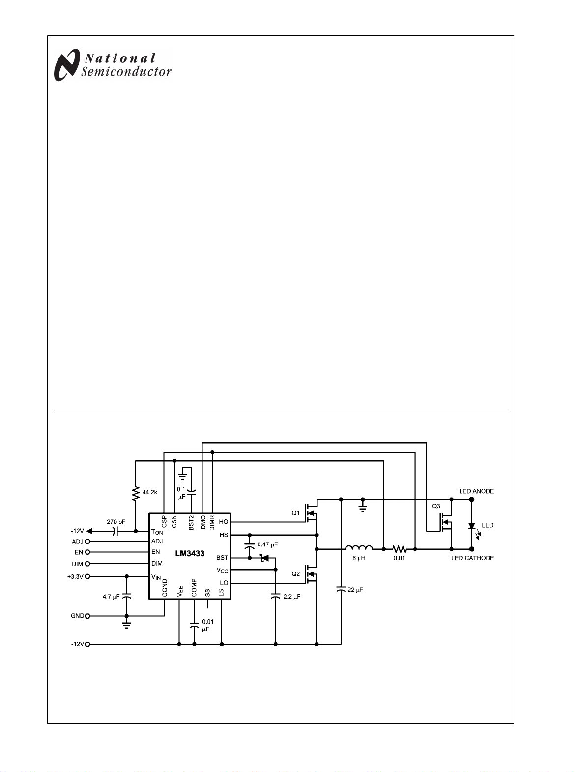
Typical Application Circuit
Features
Operating input voltage range of -9V to -14V w.r.t. LED
■
anode
Control inputs are referenced to the LED anode
■
Output current greater than 6A
■
Greater than 30kHz PWM frequency capable
■
Negative output voltage capability allows LED anode to be
■
tied directly to chassis for maximum heat sink efficacy
No output capacitor required
■
Up to 1MHz switching frequency
■
Low IQ, 1mA typical
■
Soft start
■
Adaptive programmable ON time allows for constant ripple
■
current
LLP-24 package
■
Applications
LCD backlighting
■
Projection systems
■
Solid state lighting
■
Automotive lighting
■
30031531
© 2008 National Semiconductor Corporation 300315 www.national.com
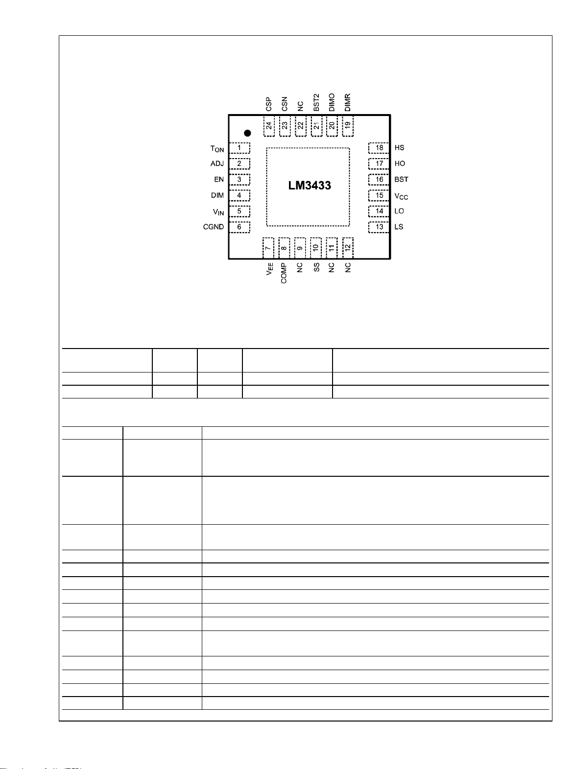
Connection Diagram
LM3433
Top View
NS Package Number SQA24A
24-Lead LLP
30031504
Ordering Information
Order Number Spec. Package
Type
LM3433SQ NOPB LLP-24 SQA24A 1000 Units, Tape and Reel
LM3433SQX NOPB LLP-24 SQA24A 4500 Units, Tape and Reel
NSC Package
Drawing
Supplied As
Pin Descriptions
Pin Name Function
On-time programming pin. Tie an external resistor (RON) from TON to CSN, and a capacitor
1
2 ADJ
3 EN
4 DIM Logic level input for LED PWM dimming. DIM is internally tied to CGND through a 100k resistor.
5 V
6 CGND Chassis ground connection.
7 V
8 COMP
9 NC No internal connection. Tie to VEE or leave open.
10 SS
11 NC No internal connection. Tie to VEE or leave open.
12 NC No internal connection. Tie to VEE or leave open.
13 LS Low side FET gate drive return pin.
14 LO Low side FET gate drive output. Low in shutdown.
T
ON
IN
EE
(CON) from TON to VEE. This sets the nominal operating frequency when the LED is fully
illuminated.
Analog LED current adjust. Tie to VIN for fixed 60mV average current sense resistor voltage. Tie
to an external reference to adjust the average current sense resistor voltage (programmed output
current). Refer to the "V
Characteristics section and the Design Procedure section of the datasheet.
Enable pin. Connect this pin to logic level HI or VIN for normal operation. Connect this pin to
CGND for low current shutdown. EN is internally tied to VIN through a 100k resistor.
Logic power input: Connect to positive voltage between +3.0V and +5.8V w.r.t. CGND.
Negative voltage power input: Connect to voltage between –14V to –9V w.r.t. CGND.
Compensation pin. Connect a capacitor between this pin and VEE.
Soft Start pin. Tie a capacitor from SS to VEE to reduce input current ramp rate. Leave pin open
if function is not used. The SS pin is pulled to VEE when the device is not enabled.
vs. ADJ Voltage" graphs in the Typical Performance
SENSE
www.national.com 2

Pin Name Function
15
V
CC
Low side FET gate drive power bypass connection and boost diode anode connection. Tie a
2.2µF capacitor between VCC and VEE.
16 BST High side "synchronous" FET drive bootstrap rail.
17 HO High side "synchronous" FET gate drive output. Pulled to HS in shutdown.
18 HS Switching node and high side "synchronous" FET gate drive return.
19 DIMR LED dimming FET gate drive return. Tie to LED cathode.
20 DIMO LED dimming FET gate drive output. DIMO is a driver that switches between DIMR and BST2.
21 BST2 DIMO high side drive supply pin. Tie a 0.1µF between BST2 and CGND.
22 NC No internal connection. Tie to VEE or leave open.
23 CSN Current sense amplifier inverting input. Connect to current sense resistor negative terminal.
24 CSP Current sense amplifier non-inverting input. Connect to current sense resistor positive terminal.
EP
V
EE
Exposed Pad on the underside of the device. Connect this pad to a PC board plane connected
to VEE.
Block Diagram
LM3433
30031503
3 www.national.com
Absolute Maximum Ratings (Note 1)
If Military/Aerospace specified devices are required,
LM3433
please contact the National Semiconductor Sales Office/
Distributors for availability and specifications.
VIN, EN, DIM, ADJ to CGND
COMP, SS to V
BST to HS -0.3V to +7V
VCC to V
CGND, DIMR, CSP, CSN,
TON to V
HS to VEE (Note 2)
LS to V
EE
HO output HS-0.3V to BST+0.3V
DIMO to DIMR -0.3V to +7V
LO output LS-0.3V to VCC +0.3V
BST2 to V
Maximum Junction
EE
EE
EE
EE
-0.3V to +7.5V
-0.3V to +16V
-0.3V to +16V
-0.3V to +0.3V
-0.3V to 22.0V
-0.3V to +7V
-0.3V to +7V
150°C
Power Dissipation(Note 3) Internally Limited
ESD Susceptibility
(Note 4)
Human Body Model 2kV
Machine Model 200V
Charge Device Model 1kV
Operating Conditions
Operating Junction
Temperature Range (Note 5) −40°C to +125°C
Storage Temperature −65°C to +150°C
Input Voltage VIN w.r.t. CGND 3.0V to 5.8V
Input Voltage VEE w.r.t. CGND -9V to -14V
ADJ Input Voltage Range to
CGND
CSP, CSN Common Mode
Range With Respect to CGND
Temperature
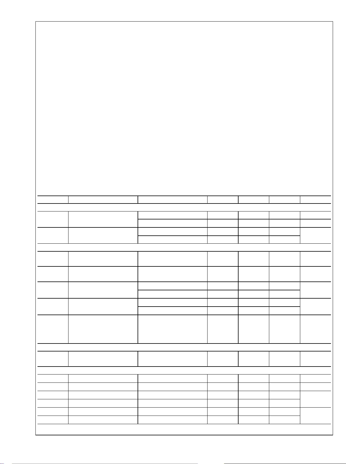
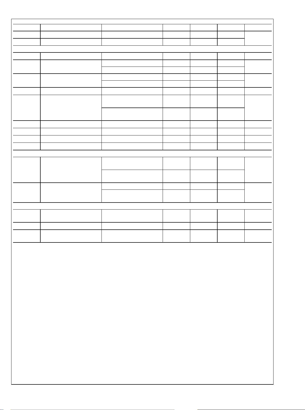
Electrical Characteristics
Specifications in standard type face are for TJ = 25°C and those with boldface type apply over the full Operating Temperature
Range ( TJ = −40°C to +125°C). Minimum and Maximum limits are guaranteed through test, design, or statistical correlation. Typical
values represent the most likely parametric norm at TJ = +25ºC, and are provided for reference purposes only. Unless otherwise
stated the following conditions apply: VEE = -12.0V and VIN = +3.3V with respect to CGND.
Symbol Parameter Conditions
SUPPLY CURRENT
IINV
EE
VEE Quiescent Current EN = CGND 3 19 µA
EN = VIN, Not Switching 1.0 mA
IINV
IN
VIN Quiescent Current EN = VIN, Not Switching 300
EN = CGND 35 71
OUTPUT CURRENT CONTROL
V
CS
G
ADJ
I
CSN
I
CSP
Gm CS to COMP
Current sense target voltage;
VCS = V
I
ADJ
(V
CNP-VCSN
– V
CSP
Gain = (V
)
CSN
-CGND)/
ADJ
Isense Input Current V
Isense Input Current V
V
= V
ADJ
IN
VIN = 3.3V, V
ADJ
w.r.t. CGND
= 1V w.r.t. CGND -50
ADJ
V
= V
ADJ
IN
= V
ADJ
IN
V
= 1V w.r.t. CGND 1
ADJ
Transconductance; Gm =
I
/ (V
– V
- V
COMP
CSP
CSN
ADJ
/
16.67)
ON TIME CONTROL
T
ONTH
On time threshold V
- VEE at terminate ON time
T
ON
event
GATE DRIVE AND INTERNAL REGULATOR
V
CCOUT
V
CCILIM
R
OLH
R
OHH
R
OLL
R
OHL
VCC output regulation w.r.t. VEEICC = 0mA to 20mA
VCC current limit VCC = V
EE
HO output low resistance I = 50mA source
HO output high resistance I = 50mA sink
LO output low resistance I = 50mA source
LO output high resistance I = 50mA sink
= 0.5V or 1.5V
Min(Note 5) Typ(Note 6) Max(Note 5)
57 60 63 mV
15 16.67 18 V/V
10
60
0.6 1.3 2.2 mS
230 287 334 mV
6.3 6.75 7.1 V
33 53 mA
2
3
2
3
0V to V
-6V to 0V
Units
µA
µA
µA
Ω
Ω
IN
www.national.com 4
LM3433
Symbol Parameter Conditions
R
OLP
R
OHP
DIMO output low resistance I = 5mA source
DIMO output high resistance I = 5mA sink
FUNCTIONAL CONTROL
V
INUVLO
V
CCUVLO
V
EN
R
EN
V
DIM
VIN undervoltage lockout With respect to CGND 1.4 V
VCC - VEE undervoltage lockout
thresholds
Enable threshold, with respect
to CGND
On Threshold 6.0 6.6 7.0
Off threshold 4.9 5.4 5.8
Device on w.r.t. CGND 1.6
Device off w.r.t. CGND 0.6
Enable pin pullup resistor 100
DIM logic input threshold DIM rising threshold w.r.t.
CGND
DIM falling threshold w.r.t.
CGND
R
I
I
R
DIM
ADJ
SS
SS
DIM pin pulldown resistor 100
ADJ pin current -1.0
SS pin source current
SS pin pulldown resistance EN = CGND
AC SPECIFICATIONS
T
DTD
LO and HO dead time LO falling to HO rising dead
time
HO falling to LO rising dead
time
T
PDIM
DIM to DIMO propagation
delay
DIM rising to DIMO rising delay 68 124
DIM falling to DIMO falling
delay
THERMAL SPECIFICATIONS
T
JLIM
Junction temperature thermal
limit
T
JLIM(hyst)
θ
JA
Thermal limit hysteresis 20
LLP-24 package thermal
JEDEC 4 layer board
resistance
Min(Note 5) Typ(Note 6) Max(Note 5)
20
30
1.6
0.6
10
1.0
26
28
58 160
175 °C
39 °C/W
Units
Ω
V
V
kΩ
V
kΩ
1.0 µA
µA
kΩ
ns
ns
°C
Note 1: Absolute maximum ratings are limits beyond which damage to the device may occur. Operating Ratings are conditions for which the device is intended
to be functional, but device parameter specifications may not be guaranteed. For guaranteed specifications and test conditions, see the Electrical Characteristics.
Note 2: The HS pin can go to -6V with respect to VEE for 30ns and +22V with respect to VEE for 50ns without sustaining damage.
Note 3: The maximum allowable power dissipation is a function of the maximum junction temperature, TJ(MAX), the junction-to-ambient thermal resistance,
θJA, and the ambient temperature, TA. The maximum allowable power dissipation at any ambient temperature is calculated using: PD (MAX) = (T
θJA. Exceeding the maximum allowable power dissipation will cause excessive die temperature, and the regulator will go into thermal shutdown. Internal thermal
shutdown circuitry protects the device from permanent damage. Thermal shutdown engages at TJ=175°C (typ.) and disengages at TJ=155°C (typ).
Note 4: Human Body Model, applicable std. JESD22-A114-C. Machine Model, applicable std. JESD22-A115-A. Field Induced Charge Device Model, applicable
std. JESD22-C101-C.
Note 5: All limits guaranteed at room temperature (standard typeface) and at temperature extremes (bold typeface). All room temperature limits are 100%
production tested. All limits at temperature extremes are guaranteed via correlation using standard Statistical Quality Control (SQC) methods. All limits are used
to calculate Average Outgoing Quality Level (AOQL).
Note 6: Typical numbers are at 25°C and represent the most likely norm.
5 www.national.com
J(MAX)
− TA)/

Typical Performance Characteristics
LM3433
Efficiency vs. LED Forward Voltage
(V
CGND-VEE
= 9V)
Efficiency vs. LED Forward Voltage
(V
CGND-VEE
= 14V)
30031523
Efficiency vs. LED Forward Voltage
(V
CGND-VEE
V
SENSE
= 12V)
vs. V
(VIN = 3.3V)
ADJ
30031522
30031521
V
vs. V
SENSE
(VIN = 5.0V)
www.national.com 6
ADJ
30031519
V
vs. Temperature
SENSE
(ADJ = VIN)
30031518
30031524

V
vs. Temperature
SENSE
(ADJ = 1.0V)
Average LED Current vs. DIM Duty Cycle
(30kHz dimming, I
= 6A nominal)
LED
LM3433
30031525
Startup Waveform
I
= 6A nominal, VIN = 3.3V, VEE = -12V, V
LED
Top trace: EN input, 2V/div, DC
Middle trace: VEE input current, 2A/div, DC
Bottom trace: I
, 2A/div, DC
LED
T = 100µs/div
LED
30031567
= 3V, SS = open
30kHz PWM Dimming Waveform Showing Inductor Ripple
Current
Shutdown Waveform
I
= 6A nominal, VIN = 3.3V, VEE = -12V, V
LED
Top trace: EN input, 2V/div, DC
Middle trace: VEE input current, 2A/div, DC
Bottom trace: I
T = 100µs/div
, 2A/div, DC
LED
= 3V, SS = open
LED
30031520
30031568
I
= 6A nominal, VIN = 3.3V, VEE = -12V
LED
Top trace: DIM input, 2V/div, DC
Bottom trace: I
, 2A/div, DC
LED
T = 10µs/div
30031566
7 www.national.com

Operation
LM3433
CURRENT REGULATOR OPERATION
The LM3433 is a controller for a Continuous Conduction Buck
Converter. Because of its buck topology and operation in the
continuous mode, the output current is very well controlled. It
only varies within a switching frequency cycle by the inductor
ripple current. This ripple current is normally set at 10% of the
DC current. Setting the ripple current lower than 10% is a
useful tradeoff of inductor size for less LED light output ripple.
Additional circuitry can be added to achieve any LED light
ripple desired.
The LED current is set by the voltage across a sense resistor.
This sense voltage is nominally 60mV but can be programmed higher or lower by an external control voltage.
The running frequency of the converter is programmed by an
external RC network in conjunction with the LED's forward
voltage. The frequency is nominally set around 200kHz to
500khz. Fast PWM control is available by shorting the output
of the current source by a MOSFET in parallel with the LED.
During the LED OFF time the running frequency is determined
by the RC network and the parasitic resistance of the output
circuit including the DIM FET R
The LM3433 system has been evaluated to be a very accurate, high compliance current source. This is manifest in its
high output impedance and accurate current control. The current is measured to vary less than 6mA out of 6A when
transitioning from LED OFF (output shorted) to LED ON (output ~6V).
PROTECTION
The LM3433 has dedicated protection circuitry running during
normal operation. The thermal shutdown circuitry turns off all
power devices when the die temperature reaches excessive
levels. The VCC undervoltage lockout (UVLO) comparator
protects the power devices during power supply startup and
shutdown to prevent operation at voltages less than the minimum operating input voltage. The VCC pin is short circuit
protected to VEE. The LM3433 also features a shutdown mode
which decreases the supply current to approximately 35µA.
The ADJ, EN, and DIM pins are capable of sustaining up to
+/-2mA. If the voltages on these pins will exceed either VIN or
CGND by necessity or by a potential fault, an external resistor
is recommended for protection. Size this resistor to limit pin
current to under 2mA. A 10k resistor should be sufficient. This
resistor may be used in any application for added protection
without any impact on function or performance.
DESIGN PROCEDURE
This section presents guidelines for selecting external components.
DSON
.
FIXED LED CURRENT
The ADJ pin sets V
internal reference for V
current based on the following equation:
. Tie ADJ to VIN to use a fixed 60mV
SENSE
SENSE
. Select R
to fix the LED
SENSE
ADJUSTABLE LED CURRENT
When tied to an external voltage the ADJ pin sets V
based on the following equation:
When the reference on ADJ is adjustable, V
can be adjusted within the linear range of the ADJ pin. This
SENSE
SENSE
and I
LED
range has the following limitations:
When V
anteed by design to be less than or equal to 0.3V/16.667.
When V
VIN - 1V, V
equal to V
V
SENSE
is less than this linear range the V
ADJ
is greater than this linear range and less than
ADJ
switches to 60mV.
is guaranteed by design to be less than or
SENSE
/16.667. If V
ADJ
is greater than VIN - 1V,
ADJ
SENSE
is guar-
INPUT CAPACITOR SELECTION
A low ESR ceramic capacitor is needed to bypass the MOSFETs. This capacitor is connected between the drain of the
synchronous FET (CGND) and the source of the main switch
(VEE). This capacitor prevents large voltage transients from
appearing at the VEE pin of the LM3433. Use a 22µF value
minimum with X5R or X7R dielectric. In addition to the FET
bypass capacitors, additional bypass capacitors should be
placed near the VEE and VIN pins and should be returned to
CGND.
The input capacitor must also be sized to handle the dimming
frequency input ripple when the DIM function is used. This
ripple may be as high as 85% of the nominal DC input current
(at 50% duty cycle). When dimming this input capacitor
should be selected to handle the input ripple current.
RECOMMENDED OPERATING FREQUENCY AND ON TIME "TIMEON" CALCULATION
Although the switching frequency can be set over a wide
range, the following equation describes the recommended
frequency selection given inexpensive magnetic materials
available today:
SETTING LED CURRENT CONTROL
LM3433 uses average current mode control to regulate the
current delivered to the LED (I
resistor (R
I
into a voltage that is sensed by the LM3433 at the CSP
LED
and CSN pins. CSP and CSN are the inputs to an error am-
) in series with the LED is used to convert
SENSE
plifier with a programmed input offset voltage (V
V
is used to regulate I
SENSE
tion:
www.national.com 8
). An external current sense
LED
based on the following equa-
LED
SENSE
).
In the above equation A=1.2 for powdered iron core inductors
and A=0.9 or less for ferrite core inductors. This difference
takes into account the fact that ferrite cores generally become
more lossy at higher frequencies. Given the switching frequency f calculated above, TIMEON can be calculated. If
V
is the forward voltage drop of the LED that is being driv-
LED
en, TIMEON can be calculated with the following equation:

LM3433
TIMING COMPONENTS (RON and CON)
Using the calculated value for TIMEON, the timing components RON and CON can be selected. CON should be large
enough to dominate the parasitic capacitance of the TON pin.
A good CON value for most applications is 1nF. Based on calculated TIMEON, CON, and the nominal VEE and V
RON can be calculated based on the following equation:
voltages,
LED
INDUCTOR SELECTION
The most critical inductor parameters are inductance, current
rating, and DC resistance. To calculate the inductance, use
the desired peak to peak LED ripple current (I
and CON. A reasonable value for I
inductor value is calculated using the following equation:
For all V
and is only dependent on the passive external compo-
and VEE voltages, I
LED
is 10% of I
RIPPLE
remains constant
RIPPLE
RIPPLE
), RON,
. The
LED
nents RON, CON, and L.
The I2R loss caused by the DC resistance of the inductor is
an important parameter affecting the efficiency. Lower DC resistance inductors are larger. A good tradeoff point between
the efficiency and the core size is letting the inductor I2R loss
equal 1% to 2% of the output power. The inductor should have
a current rating greater than the peak current for the application. The peak current is I
plus 1/2 I
LED
RIPPLE
.
POWER FET SELECTION
FETs should be chosen so that the I2R
1% of the total output power. Analysis shows best efficiency
with around 8mΩ of R
application. All of the switching loss is in the main switch FET.
and 15nC of gate charge for a 6A
DSON
loss is less than
DSON
An additional important parameter for the synchronous FET
is reverse recovery charge (QRR). High QRR adversely affects
the transient voltages seen by the IC. A low QRR FET should
be used.
DIM FET SELECTION
Choose a DIM FET with the lowest R
cieny and low input current draw during the DIM cycle. The
for maximum effi-
DSON
output voltage during DIM will determine the switching frequency. A lower output voltage results in a lower switching
frequency. If the lower frequency during DIM must be bound,
choose a FET with a higher R
quency higher during the DIM cycle.
to force the switching fre-
DSON
BOOTSTRAP CAPACITORS
The LM3433 uses two bootstrap capacitors and a bypass capacitor on VCC to generate the voltages needed to drive the
external FETs. A 2.2µF ceramic capacitor or larger is recommended between the VCC and LS pins. A 0.47µF is recommended between the HS and BST pins. A 0.1µF is
recommended between BST2 and CGND.
SOFT-START CAPACITOR
The LM3433 integrates circuitry that, when used in conjunction with the SS pin, will slow the current ramp on start-up.
The SS pin is used to tailor the soft-start for a specific application. A capacitor value of 0.1µF on the SS pin will yield a
12mS soft start time. For most applications soft start is not
needed.
ENABLE OPERATION
The EN pin of the LM3433 is designed so that it may be controlled using a 1.6V or higher logic signal. If the enable function is not used, the EN pin may be tied to VIN or left open.
This pin is pulled to VIN internally through a 100k pull up resistor.
PWM DIM OPERATION
The DIM pin of the LM3433 is designed so that it may be controlled using a 1.6V or higher logic signal. The PWM frequency easily accomodates more than 40kHz dimming and can be
much faster if needed. If the PWM DIM pin is not used, tie it
to CGND or leave it open. The DIM pin is tied to CGND internally through a 100k pull down resistor.
LAYOUT CONSIDERATIONS
The LM3433 is a high performance current driver so attention
to layout details is critical to obtain maximum performance.
The most important PCB board design consideration is minimizing the loop comprised by the main FET, synchronous
FET, and their associated decoupling capacitor(s). Place the
VCC bypass capacitor as near as possible to the LM3433.
Place the PWM dimming/shunt FET as close to the LED as
possible. A ground plane should be used for power distribution to the power FETs. Use a star ground between the
LM3433 circuitry, the synchronous FET, and the decoupling
capacitor(s). The EP contact on the underside of the package
must be connected to VEE. The two lines connecting the sense
resistor to CSN and CSP must be routed as a differential pair
directly from the resistor. A Kelvin connection is recommended. It is good practice to route the DIMO/DIMR, HS/HO, and
LO/LS lines as differential pairs. The most important PCB
board design consideration is minimizing the loop comprised
by the main FET, synchronous FET, and their associated decoupling capacitor(s). Optimally this loop should be orthogonal to the ground plane.
9 www.national.com

Application Information
LM3433
30031516
FIGURE 1. 2A to 6A Output Application Circuit
FIGURE 2. 2A to 14A Output Application Circuit
www.national.com 10
30031517

Some Recommended Inductors (Others May Be Used)
Manufacturer Inductor Contact Information
Coilcraft GA3252-AL and SER1360 series www.coilcraft.com
800-322-2645
Coiltronics HCLP2 series www.coiltronics.com
Pulse PB2020 series www.pulseeng.com
Some Recommended Input/Bypass Capacitors (Others May Be Used)
Manufacturer Capacitor Contact Information
Vishay Sprague 293D, 592D, and 595D series tantalum www.vishay.com
407-324-4140
Taiyo Yuden High capacitance MLCC ceramic www.t-yuden.com
408-573-4150
Cornell Dubilier
MuRata High capacitance MLCC ceramic www.murata.com
Manufacturer Inductor Contact Information
Siliconix Si7386DP (Main FET, DIM FET)
ON Semiconductor NTMFS4841NHT1G (Main FET, Synchronous FET, DIM
ESRD seriec Polymer Aluminum Electrolytic
SPV and AFK series V-chip series
Some Recommended MOSFETs (Others May Be Used)
Si7668ADP (Synchronous FET)
FET)
www.cde.com
www.vishay.com/company/brands/
siliconix/
www.onsemi.com
LM3433
11 www.national.com
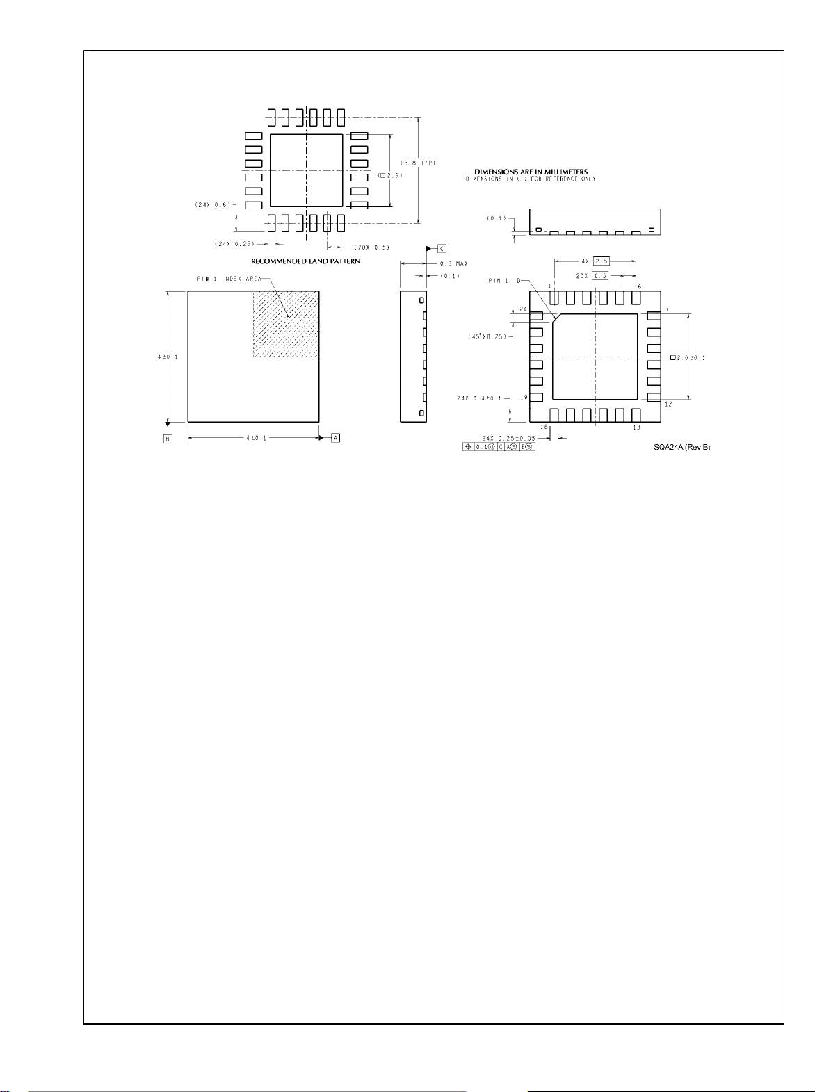
Physical Dimensions inches (millimeters) unless otherwise noted
LM3433
For Ordering, Refer to Ordering Information Table
LLP-24 Pin Package (SQA)
NS Package Number SQA24A
www.national.com 12

Notes
LM3433
13 www.national.com

Notes
For more National Semiconductor product information and proven design tools, visit the following Web sites at:
Products Design Support
Amplifiers www.national.com/amplifiers WEBENCH www.national.com/webench
Audio www.national.com/audio Analog University www.national.com/AU
Clock Conditioners www.national.com/timing App Notes www.national.com/appnotes
Data Converters www.national.com/adc Distributors www.national.com/contacts
Displays www.national.com/displays Green Compliance www.national.com/quality/green
Ethernet www.national.com/ethernet Packaging www.national.com/packaging
Interface www.national.com/interface Quality and Reliability www.national.com/quality
LVDS www.national.com/lvds Reference Designs www.national.com/refdesigns
Power Management www.national.com/power Feedback www.national.com/feedback
Switching Regulators www.national.com/switchers
LDOs www.national.com/ldo
LED Lighting www.national.com/led
PowerWise www.national.com/powerwise
Serial Digital Interface (SDI) www.national.com/sdi
Temperature Sensors www.national.com/tempsensors
Wireless (PLL/VCO) www.national.com/wireless
THE CONTENTS OF THIS DOCUMENT ARE PROVIDED IN CONNECTION WITH NATIONAL SEMICONDUCTOR CORPORATION
(“NATIONAL”) PRODUCTS. NATIONAL MAKES NO REPRESENTATIONS OR WARRANTIES WITH RESPECT TO THE ACCURACY
OR COMPLETENESS OF THE CONTENTS OF THIS PUBLICATION AND RESERVES THE RIGHT TO MAKE CHANGES TO
SPECIFICATIONS AND PRODUCT DESCRIPTIONS AT ANY TIME WITHOUT NOTICE. NO LICENSE, WHETHER EXPRESS,
IMPLIED, ARISING BY ESTOPPEL OR OTHERWISE, TO ANY INTELLECTUAL PROPERTY RIGHTS IS GRANTED BY THIS
DOCUMENT.
TESTING AND OTHER QUALITY CONTROLS ARE USED TO THE EXTENT NATIONAL DEEMS NECESSARY TO SUPPORT
NATIONAL’S PRODUCT WARRANTY. EXCEPT WHERE MANDATED BY GOVERNMENT REQUIREMENTS, TESTING OF ALL
PARAMETERS OF EACH PRODUCT IS NOT NECESSARILY PERFORMED. NATIONAL ASSUMES NO LIABILITY FOR
APPLICATIONS ASSISTANCE OR BUYER PRODUCT DESIGN. BUYERS ARE RESPONSIBLE FOR THEIR PRODUCTS AND
APPLICATIONS USING NATIONAL COMPONENTS. PRIOR TO USING OR DISTRIBUTING ANY PRODUCTS THAT INCLUDE
NATIONAL COMPONENTS, BUYERS SHOULD PROVIDE ADEQUATE DESIGN, TESTING AND OPERATING SAFEGUARDS.
EXCEPT AS PROVIDED IN NATIONAL’S TERMS AND CONDITIONS OF SALE FOR SUCH PRODUCTS, NATIONAL ASSUMES NO
LIABILITY WHATSOEVER, AND NATIONAL DISCLAIMS ANY EXPRESS OR IMPLIED WARRANTY RELATING TO THE SALE
AND/OR USE OF NATIONAL PRODUCTS INCLUDING LIABILITY OR WARRANTIES RELATING TO FITNESS FOR A PARTICULAR
PURPOSE, MERCHANTABILITY, OR INFRINGEMENT OF ANY PATENT, COPYRIGHT OR OTHER INTELLECTUAL PROPERTY
RIGHT.
LIFE SUPPORT POLICY
NATIONAL’S PRODUCTS ARE NOT AUTHORIZED FOR USE AS CRITICAL COMPONENTS IN LIFE SUPPORT DEVICES OR
SYSTEMS WITHOUT THE EXPRESS PRIOR WRITTEN APPROVAL OF THE CHIEF EXECUTIVE OFFICER AND GENERAL
COUNSEL OF NATIONAL SEMICONDUCTOR CORPORATION. As used herein:
Life support devices or systems are devices which (a) are intended for surgical implant into the body, or (b) support or sustain life and
whose failure to perform when properly used in accordance with instructions for use provided in the labeling can be reasonably expected
to result in a significant injury to the user. A critical component is any component in a life support device or system whose failure to perform
can be reasonably expected to cause the failure of the life support device or system or to affect its safety or effectiveness.
National Semiconductor and the National Semiconductor logo are registered trademarks of National Semiconductor Corporation. All other
brand or product names may be trademarks or registered trademarks of their respective holders.
Copyright© 2008 National Semiconductor Corporation
For the most current product information visit us at www.national.com
National Semiconductor
Americas Technical
Support Center
LM3433 Common Anode Capable High Brightness LED Driver with High Frequency Dimming
www.national.com
Email:
new.feedback@nsc.com
Tel: 1-800-272-9959
National Semiconductor Europe
Technical Support Center
Email: europe.support@nsc.com
German Tel: +49 (0) 180 5010 771
English Tel: +44 (0) 870 850 4288
National Semiconductor Asia
Pacific Technical Support Center
Email: ap.support@nsc.com
National Semiconductor Japan
Technical Support Center
Email: jpn.feedback@nsc.com
 Loading...