

Page 1

July 31, 2008
LM3421, LM3423
N-Channel Controllers for Constant Current LED Drivers
LM3421, LM3423 N-Channel Controllers for Constant Current LED Drivers
General Description
The LM3421/LM3423 devices are versatile high voltage LED
driver controllers. With the capability to be configured in a
Buck, Boost, Buck-Boost (Flyback), or SEPIC topology, and
an input operating voltage rating of 75V, these controllers are
ideal for illuminating LEDs in a very diverse, large family of
applications.
Adjustable high-side current sense with a typical sense voltage of 100mV allows for tight regulation of the LED current
with the highest efficiency possible. Output LED current regulation is based on peak current-mode control with predictive
Off-Time Control. This method of control eases the design of
loop compensation while providing inherent input voltage
feed-forward compensation.
The LM3421/LM3423 include a high-voltage startup regulator
that operates over a wide input range of 4.5V to 75V. The
internal PWM controller is designed for adjustable switching
frequencies of up to 2.0MHz, thus enabling compact solutions. Additional features include: “zero” current shutdown,
precision reference, logic compatible DIM input suitable for
fast PWM dimming, cycle-by-cycle current limit, and thermal
shutdown.
The LM3423 also includes an LED output status flag, a fault
flag, a programmable fault timer, and a logic input to select
the polarity of the dimming output driver.
Features
VIN range from 4.5V to 75V
■
2% Internal reference voltage (1.235V)
■
Current sense voltage adjustable from 20mV
■
High-side current sensing
■
2Ω MOSFET gate driver
■
Dimming MOSFET gate driver
■
Input under-voltage protection
■
Over-voltage protection
■
Low shutdown current, IQ < 1µA
■
Fast (50kHz) PWM dimming
■
Cycle-by-cycle current limit
■
Programmable switching frequency
■
LED output status flag (LM3423 only)
■
Fault timer pin (LM3423 only)
■
TSSOP EP 16-lead package (LM3421)
■
TSSOP EP 20-lead package (LM3423)
■
Applications
LED Drivers
■
Constant-Current Buck-Boost Regulator
■
Constant-Current Boost Regulator
■
Constant-Current Flyback Regulator
■
Constant-Current SEPIC Regulator
■
Thermo-Electric Cooler (Peltier) Driver
■
Typical Application Circuit
Boost LED Driver
© 2008 National Semiconductor Corporation 300673 www.national.com
30067331
Page 2

Connection Diagrams
Top View
LM3421, LM3423
16-Lead TSSOP EP
NS Package Number MXA16A
30067304
NS Package Number MXA20A
Ordering Information
Order Number Spec. Package Type NSC Package
Drawing
LM3421MH NOPB TSSOP-16 EP MXA16A 92 Units, Rail
LM3421MHX NOPB TSSOP-16 EP MXA16A 2500 Units, Tape and Reel
LM3423MH NOPB TSSOP-20 EP MXA20A 73 Units, Rail
LM3423MHX NOPB TSSOP-20 EP MXA20A 2500 Units, Tape and Reel
Top View
20-Lead TSSOP EP
Supplied As
30067366
Pin Descriptions
LM3423 LM3421 Name Function
1 1
2 2 EN
3 3 COMP
4 4 CSH
5 5 RCT
6 6 AGND
7 7 OVP
8 8 nDIM
9 - FLT
V
Power supply input (4.5V-75V). Bypass with 100nF capacitor to AGND as close to the device
IN
as possible in the circuit board layout.
Enable: Pull to ground for zero current shutdown. Tie directly to VIN for automatic startup at
4.1V.
Compensation: PWM controller error amplifier compensation pin. This pin connects through
a series resistor-capacitor network to AGND.
Current Sense High: Output of the high side sense amplifier and input to the main regulation
loop error amplifier.
Resistor Capacitor Timing: External RC network sets the predictive “off-time” and thus the
switching frequency. The RC network should be placed as close to the device as possible in
the circuit board layout.
Analog Ground: The proper place to connect the compensation and timing capacitor returns.
This pin should be connected via the circuit board to the PGND pin through the EP copper
circuit board pad.
Over-Voltage Protection sense input: 1.24V threshold with hysteresis that is user
programmable by the selection of the OVP Over-Voltage Lock-Out (OVLO) resistor divider
network.
Not DIM input: Dual function pin. Primarily used as the Pulse Width Modulation (PWM) input.
When driven with a resistor divider from VIN, this pin also functions as a user programmable
VIN Under-Voltage Lock-Out (UVLO) with 1.24V threshold and programmable hysteresis by
the UVLO resistor divider network. The PWM and UVLO functions can be performed
simultaneously.
Fault flag: This is an N-channel MOSFET open drain output. The FLT pin transitions to the
high (open) state once the Fault Timer has timed out and latched the controller off.
www.national.com 2
Page 3

LM3423 LM3421 Name Function
Fault Timer: The fault timer is comprised of an external capacitor, an internal charging current
10 - TIMR
source, an internal discharge N-channel MOSFET, and a comparator that latches the fault
condition when the threshold voltage (1.24V) is exceeded.
11 - LRDY
12 - DPOL
LED Ready status flag: This is an N-channel MOSFET open drain output which pulls down
whenever the LED current is not in regulation.
Dim Polarity: Selects the polarity of the DIM driver output. Tie to VCC or leave open for low
side dimming, tie to ground for high side dimming.
13 9 DDRV External Dimming MOSFET Gate Drive: Gate driver output responding to nDIM input.
14 10 PGND
Power Ground: GATE and DDRV gate drive ground current return pin. This pin should be
connected via the circuit board to the AGND pin through the EP copper circuit board pad.
15 11 GATE Main switching MOSFET gate drive output.
16 12
V
Internal Regulator Bypass: 6.9V low dropout linear regulator output. Bypass with a 2.2µF–
CC
3.3µF, ceramic type capacitor to PGND.
Main Switch Current Sense input: This pin is used for current mode control and cycle-by-cycle
17 13 IS
current limit. This pin can be tied to the drain of the main N-channel MOSFET switch for
R
sensing or tied to a sense resistor installed in the source of the same device.
DS(ON)
Resistor Pull-Down: This is an open drain N-channel MOSFET which is used to pull-down the
18 14 RPD
low side of all external resistor dividers (VIN UVLO, OVP). This pin allows for system “zerocurrent” shutdown.
High Side Sense Positive: LED current sense positive input. An external resistor sets a
reference current flowing into this pin from the programmed high-side sense voltage. Although
19 15 HSP
the current into this pin can be set to values ranging from 10µA through 1mA, a value of 100µA
is recommended. This pin is a virtual ground whose potential is set by the voltage on the HSN
pin.
High Side Sense Negative: This pin sets the reference voltage for the HSP input. An external
20 16 HSN
resistor of the same value as that used on the HSP pin should be connected from this pin to
the negative side of the current sense resistor.
EP (21) EP (17) EP
EP: Star ground, connecting AGND and PGND. For thermal considerations please refer to
(Note 4) of the Electrical Characteristics table.
LM3421, LM3423
3 www.national.com
Page 4

Absolute Maximum Ratings (Notes 1, 2)
If Military/Aerospace specified devices are required,
please contact the National Semiconductor Sales Office/
Distributors for availability and specifications.
VIN, EN, RPD, nDIM -0.3V to 76.0V
LM3421, LM3423
OVP, HSP, HSN, LRDY, FLT,
DPOL
RCT -0.3V to 76.0V
-1mA to +5mA continuous
IS -0.3V to 76.0V
V
CC
TIMR -0.3V to 7.0V
COMP, CSH -0.3V to 6.0V
GATE, DDRV -0.3V to V
-1mA continuous
-0.3V to 76.0V
-100µA continuous
-2V for 100ns
-1mA continuous
-0.3V to 8.0V
-100µA to +100µA
-200µA to +200µA
Continuous
Continuous
CC
PGND -0.3V to 0.3V
-2.5V to 2.5V for 100ns
Maximum Junction
Temperature (Internally
Limited)
Storage Temperature Range −65°C to +150°C
Maximum Lead Temperature
(Soldering) (Note 5)
Continuous Power Dissipation
Internally Limited
(Notes , 4)
ESD Susceptibility
(Note 6)
Human Body Model 2kV
Machine Model 200V
Charge Device Model 500V
Operating Conditions (Notes 1, 2)
Operating Junction
Temperature Range (Note 7) −40°C to +150°C
Input Voltage V
IN
-2.5V for 100ns
VCC+2.5V for 100ns
-1mA to +1mA continuous
Electrical Characteristics (Note 2)
Specifications in standard type face are for TJ = 25°C and those with boldface type apply over the full Operating Temperature
Range ( TJ = −40°C to +125°C). Minimum and Maximum limits are guaranteed through test, design, or statistical correlation. Typical
values represent the most likely parametric norm at TJ = +25°C, and are provided for reference purposes only. Unless otherwise
stated the following condition applies: VIN = +14V.
Symbol Parameter Conditions
STARTUP REGULATOR
V
CCREG
I
CCLIM
I
Q
I
SD
VCC Regulation ICC = 0mA 6.30
VCC Current Limit VCC = 0V
Quiescent Current EN = 3.0V, Static
Shutdown Current EN = 0V 0.1 1.0
VCC SUPPLY
V
CCUV
VCC UVLO Threshold VCC Increasing
VCC Decreasing
V
CCHYS
VCC UVLO Hysteresis 0.1
EN THRESHOLDS
EN
ST
EN Startup Threshold EN Increasing 1.75 2.40
EN Decreasing 0.80 1.63
EN
R
STHYS
EN
EN Startup Hysteresis
EN Pulldown Resistance EN = 1V
CSH THRESHOLDS
CSH High Fault CSH Increasing 1.6
CSH Low Condition on LRDY
CSH increasing
Pin (LM3423 only)
OV THRESHOLDS
OVP
OVP
CB
HYS
OVP OVLO Threshold OVP Increasing
OVP Hysteresis Source
OVP Active (high)
Current
DPOL THRESHOLDS
DPOL
DPOL Logic Threshold DPOL Increasing 2.0
THRESH
Min(Note 7) Typ(Note 8) Max(Note 7)
6.90 7.35 V
20 25
2 3
4.17 4.50
3.70 4.08
0.1
0.45 0.82 1.30
1.0
1.185 1.240 1.285 V
20 23 25 µA
2.3 2.6 V
165°C
300°C
4.5V to 75V
Units
mA
µA
V
V
MΩ
V
www.national.com 4
Page 5

LM3421, LM3423
Symbol Parameter Conditions
R
DPOL
DPOL Pullup Resistance
Min(Note 7) Typ(Note 8) Max(Note 7)
500 1200
Units
KΩ
FAULT TIMER
V
I
FLT
FLTTH
Fault Threshold
Fault Pin Source Current
1.185 1.240 1.285 V
10 11.5 13 µA
ERROR AMPLIFIER
V
REF
Error Amplifier Input Bias
CSH Reference Voltage With Respect to AGND 1.210
Current
-0.6 0 0.6
1.235 1.260 V
µA
COMP Sink / Source Current 22 30 35
Transconductance 100 µA/V
Linear Input Range (Note 9) ±125 mV
Transconductance Bandwidth
(Note 9)
-6dB Unloaded Response
0.5 1.0
MHz
OFF TIMER
Minimum Off-time
R
RCT
RCT Reset Pull-down
Resistance
V
RCT
VIN/25 Reference Voltage VIN = 14V 540
f Continuous Conduction
Switching Frequency
RCT = 1V through 1kΩ
2.2nF > CT > 470pF
35 75
36 120
565 585 mV
25/(CTRT)
ns
Ω
Hz
PWM COMPARATOR
COMP to PWM Offset 700 800 900 mV
CURRENT LIMIT (IS)
I
LIM
I
Leading Edge Blanking Time 115 210 325
Current Limit Threshold 200
Delay to Output
LIM
245 300 mV
35 75
ns
HIGH SIDE TRANSCONDUCTANCE AMPLIFIER
Input Bias Current 11.5 µA
Transconductance 20 119 mA/V
Input Offset Current -1.5 0 1.5 µA
Input Offset Voltage -7 0 7 mV
Transconductance Bandwidth
(Note 9)
I
CSH
= 100µA
250 500 kHz
GATE DRIVER (GATE)
R
SRC(GATE)
R
SNK(GATE)
GATE Sourcing Resistance GATE = High
GATE Sinking Resistance GATE = Low
2.0 6.0
1.3 4.5
Ω
DIM DRIVER (DIM, DDRV)
nDIM
nDIM
R
SRC(DDRV)
R
SNK(DDRV)
VTH
HYS
nDIM / UVLO Threshold 1.185
nDIM Hysteresis Current 20
DDRV Sourcing Resistance DDRV = High
DDRV Sinking Resistance DDRV = Low
1.240 1.285 V
23 25 µA
13.5 30.0
3.5 10.0
Ω
PULL-DOWN N-CHANNEL MOSFETS
R
R
R
RPD
FLT
LRDY
RPD Pull-down Resistance
FLT Pull-down Resistance
LRDY Pull-down Resistance
145 300
145 300
135 300
Ω
THERMAL SHUTDOWN
T
SD
T
HYS
Thermal Shutdown Threshold
Thermal Shutdown Hysteresis
165
25
°C
THERMAL RESISTANCE
5 www.national.com
Page 6

Symbol Parameter Conditions
θ
JA
Junction to Ambient (Note 4) 16L TSSOP EP 37.4
Min(Note 7) Typ(Note 8) Max(Note 7)
20L TSSOP EP 34.0
θ
JC
Junction to Exposed Pad (EP) 16L TSSOP EP 2.3
20L TSSOP EP 2.3
LM3421, LM3423
Note 1: Absolute maximum ratings are limits beyond which damage to the device may occur. Operating Ratings are conditions for which the device is intended
to be functional, but device parameter specifications may not be guaranteed. For guaranteed specifications and test conditions, see the Electrical Characteristics.
Note 2: All voltages are with respect to the potential at the AGND pin, unless otherwise specified.
Note 3: Internal thermal shutdown circuitry protects the device from permanent damage. Thermal shutdown engages at TJ=165°C (typical) and disengages at
TJ=140°C (typical).
Note 4: Junction-to-ambient thermal resistance is highly board-layout dependent. The numbers listed in the table are given for an reference layout wherein the
16L TSSOP package has its EP pad populated with 9 vias and the 20L TSSOP has its EP pad populated with 12 vias. In applications where high maximum power
dissipation exists, namely driving a large MOSFET at high switching frequency from a high input voltage, special care must be paid to thermal dissipation issues
during board design. In high-power dissipation applications, the maximum ambient temperature may have to be derated. Maximum ambient temperature (T
) is dependent on the maximum operating junction temperature (T
MAX
), and the junction-to ambient thermal resistance of the package in the application (θJA), as given by the following equation: T
MAX
). In most applications there is little need for the full power dissipation capability of this advanced package. Under these circumstances, no vias would be
MAX
required and the thermal resistances would be 104 °C/W for the 16L TSSOP and 86.7 °C/W for the 20L TSSOP. It is possible to conservatively interpolate between
the full via count thermal resistance and the no via count thermal resistance with a straight line to get a thermal resistance for any number of vias in between
these two limits.
Note 5: Refer to National’s packaging website for more detailed information and mounting techniques. http://www.national.com/packaging/
Note 6: Human Body Model, applicable std. JESD22-A114-C. Machine Model, applicable std. JESD22-A115-A. Field Induced Charge Device Model, applicable
std. JESD22-C101-C.
Note 7: All limits guaranteed at room temperature (standard typeface) and at temperature extremes (bold typeface). All room temperature limits are 100%
production tested. All limits at temperature extremes are guaranteed via correlation using standard Statistical Quality Control (SQC) methods. All limits are used
to calculate Average Outgoing Quality Level (AOQL).
Note 8: Typical numbers are at 25°C and represent the most likely norm.
Note 9: These electrical parameters are guaranteed by design, and are not verified by test.
= 125°C), the maximum power dissipation of the device in the application (P
J-MAX-OP
A-MAX
= T
J-MAX-OP
Units
°C/W
°C/W
– (θJA × P
A-
D-
D-
www.national.com 6
Page 7

Typical Performance Characteristics Taken from the standard evaluation board
LM3421, LM3423
Boost Efficiency vs. Input Voltage
(6 White LEDs, ~20V at 1A)
Boost Efficiency vs. Input Voltage
(11 White LEDs, ~46V at 1A)
Buck/Boost Efficiency vs. Input Voltage
(6 White LEDs, ~20V at 1A)
30067322
30067323
Average LED Current vs. PWM DIM Duty Cycle
(VIN = 12V, 6 White LEDs, ~20V at 1A)
30067321
LED Current vs. Ambient Temperature
(VIN = 12V, Nominal LED Current Set at 1A)
30067319
30067318
LED Current vs. Input Voltage
(Boost, 6 White LEDs, ~20V at 1A)
30067324
7 www.national.com
Page 8

LM3421, LM3423
30kHz PWM Dimming
(95% Duty Cycle ON)
30kHz PWM Dimming
(10% Duty Cycle ON)
I
= 1A nominal, VIN = 12V, V
LED
LED(s)
= 20V
30067369
Top trace: nDIM input, 2V/div, DC
Bottom trace: I
, 500mA/div, DC
LED
T = 10µs/div
30kHz PWM Dimming
(5% Duty Cycle ON)
I
= 1A nominal, VIN = 12V, V
LED
LED(s)
= 20V
Top trace: nDIM input, 2V/div, DC
Bottom trace: I
, 500mA/div, DC
LED
T = 10µs/div
As shown in the Average LED Current vs. PWM DIM Duty Cycle curve the current
drops at very low duty cycle. This is due to the fact that the switcher is shut off
during the LED off time. At low duty cycle the choke does not have time to get
the current up to the control setpoint. This can be looked on as an advantage in
that it allows a wider PWM control range, albeit not linear under about 7.5% duty
cycle (this transition point can be set over a limited range by component value
selection).
30067371
I
= 1A nominal, VIN = 12V, V
LED
Top trace: nDIM input, 2V/div, DC
Bottom trace: I
, 500mA/div, DC
LED
T = 10µs/div
LED(s)
= 20V
30067370
www.national.com 8
Page 9

Block Diagram
LM3421, LM3423
30067303
9 www.national.com
Page 10

Functional Description
ENABLE
The LM3421/LM3423 devices impliment “zero-current” shutdown via the EN and RPD pins. When pulled low, the EN pin
places the devices into a near-zero current draw state in
which only leakage currents will be observed flowing into the
LM3421, LM3423
pins of the LM3421/LM3423.
The RPD pin connects to an open drain N-channel MOSFET
that is only enabled when the device is enabled. Tying the
bottom resistor of external resistor dividers, namely VIN Under-Voltage Lock-Out (UVLO) and Over-Voltage Lock-Out
(OVLO), allows them to float during shutdown, thus removing
their current paths. In this way, the LED module can be designed to draw zero current from the VIN input supply line
when disabled. All other internal pin functions are also disabled and draw zero current.
The EN pin should be tied to VIN if the low current disable
function is not desired. This pin, being a micro-power enable,
is not a precision comparator input and is not appropriate for
implementing UVLO. The nDIM pin may be used for an accurate VIN UVLO function, as discussed in detail below in the
section titled External Under-Voltage Protection.
STARTUP REGULATOR (VCC LDO)
The LM3421/LM3423 devices include a high voltage, low
dropout (LDO) bias regulator. When power is applied and the
EN pin is high, the regulator is enabled and sources current
into an external capacitor connected to the VCC pin. The output voltage is 6.9V nominally and the supply is internally
current limited to 20mA minimum. The recommended bypass
capacitance range for the VCC regulator is 2.2µF to 3.3µF.
The output of the VCC regulator is monitored by an internal
UVLO circuit. The purpose of VCC UVLO is to protect the device during startup, normal operation, and shutdown from
attempting to operate with insufficient supply voltage. During
startup, the VCC UVLO circuitry ensures that the device does
not begin switching until the VCC voltage exceeds the upper
threshold in the hysteretic band of the VCC UVLO threshold.
When VIN is low, the low dropout regulator will drive VCC to
within several hundred millivolts of VIN. If during normal operation VCC falls below the VCC UVLO threshold for any reason, the VCC UVLO circuitry will disable the device. In this
case, the device will not resume operation until the VCC UVLO
release threshold voltage is exceeded. On-chip filtering prevents intermittent transient dips that are common in high
speed switching regulators from triggering VCC UVLO.
30067356
FIGURE 1. Under-Voltage Lock-Out Circuitry
Cycling the EN Pin Causes Escape from UVLO
When the EN and RPD pins are used together to implement
the “zero-current” shutdown function, they allow the resistor
divider (R1 and R2) on the nDIM to pull the pin up to VIN. This
will appear as a legal operating voltage (nDIM > 1.24V). This
condition is removed as soon as the EN pin is taken back to
a high state. If the input voltage is inside the UVLO threshold
hysteretic window and the controller is off, cycling the EN pin
low and then high will start the controller even though the UVLO turn-on threshold has not been reached.
EXTERNAL UNDER-VOLTAGE PROTECTION
The nDIM pin is a dual-function input that features an accurate
1.24V threshold with programmable hysteresis. This pin functions as both the PWM input for fast dimming of the LEDs and
as a VIN UVLO. When the pin voltage rises and exceeds the
1.24V threshold, 23µA (typical) of current is driven out of the
nDIM pin into the resistor divider providing programmable
hysteresis. To calculate the amount of VIN hysteresis
achieved, simply multiply the top resistor in the divider (R1 in
Figure 1) by 23µA (for a two resistor system) or the Thevenin
resistance by 23µA for any other network. Note that if the
Thevenin resistance is used in the calculation the result is the
amount of voltage hysteresis observed at the nDIM pin. This
quantity must be gained up by the appropriate resistor divider
attenuation factor to calculate the actual VIN hysteresis observed.
www.national.com 10
Page 11

PROGRAMMING AVERAGE LED CURRENT
FIGURE 2. LED Current Sense Circuitry
This section serves to explain how the LM3421/LM3423 controllers use the high-side sense amplifier to regulate average
LED current. Instructions for calculation of component values
are also covered.
The voltage at the CSH pin is regulated by the error amplifier
to be 1.235V. Understanding how average LED current is
regulated requires understanding the relationship between
the CSH voltage (V
is because V
current, I
LED
SENSE
.
) and the sense voltage (V
CSH
and R
directly set the average LED
SENSE
SENSE
). This
The high side amplifier in Figure 2 forces its input terminals
to equal potential. Because of this, the V
forced across the differential voltages across R
R
. In other words, the amplifier’s output P-MOSFET tran-
HSN
sistor pulls current through R
occurs when the voltage (|V
V
. So the current flowing down to the CSH pin is given
SENSE
by:
HSP
RHSP
until V
| - |V
HSP=VHSN
SENSE
|) is equal to
RHSN
voltage is
and
HSP
, and this
And the voltage at the CSH pin is then given by:
30067357
The equation above shows how current in the LED relates to
the regulated voltage V
LM3423.
, which is 1.235V for the LM3421/
REF
The selection of resistors is not arbitrary; for matching and
noise performance we suggest that the CSH current is 100µA.
This current does not flow in the LEDs and will not affect either
the off state LED current or the regulated LED current. The
CSH current can be above or below this value, but the high
side amplifier offset characteristics may be affected slightly.
In addition, to hold an initial 5% tolerance on the LED current,
R
should be selected to have at least 50mV across it at
SENSE
the desired LED current (R
50mV / I
(P
SENSE
sense resistor value: P
). The power dissipated in the sense resistor
LED
) is directly proportional to the sense voltage and the
SENSE
greater than or equal to
SENSE
2
= I
LED
x R
SENSE
.
Design Example: The user desires 1A of average LED current. 100mV is a typical starting point for V
R
of 100mV/1A = 100mΩ. This will limit the power dis-
SENSE
sipation in R
Once a standard component value has been selected for
R
, the value of the resistor in series with the HSP pin
SENSE
(R
) can be calculated. The signal current set up by R
HSP
should be set for approximately 100µA at the desired LED
to 100mW while providing good regulation.
SENSE
, providing an
SENSE
HSP
current.
LM3421, LM3423
So, the CSH voltage is the sense voltage (V
by the ratio of R
system’s error amplifier regulates the CSH voltage (V
V
. So, using the above equation with some slight substi-
REF
tution and rearranging, we can conclude the following:
CSH
to R
. As stated previously, the control
HSP
SENSE
) gained up
) to
CSH
This leads to the final equation that can be used to calculate
average LED current given any combination of resistor values:
A resistor of equal value should be placed in series with the
HSN pin to cancel out the effects of the input bias current
(~10µA) of both inputs of the high side sense amplifier. The
signal current (100µA) set up by the HSP resistor flows into
the HSP pin and is translated down to appear as a source
current from the CSH pin. The resistor from the CSH pin to
ground (R
sen to convert the 100µA signal current representing the
) would nominally be 12.4kΩ. This value is cho-
CSH
average LED current to a voltage very close to 1.235V, the
11 www.national.com
Page 12

error amplifier’s internally programmed reference voltage
(V
).
REF
So, given the values selected, the final average LED current
can be calculated using the above equations:
LM3421, LM3423
If it is desirable to use the CSH pin as a low side current sense
input regulated to the 1.235V feedback voltage, simply tie
both HSP and HSN to ground to disable the high side sense
amplifier. An internal diode prevents reverse current flow to
the HSP and HSN pins.
CURRENT SENSE/CURRENT LIMIT
The LM3421/LM3423 devices provide current mode control
using a comparator that monitors the MOSFET transistor current, comparing it with the COMP pin voltage. Further, in
incorporates a cycle-by-cycle over-current protection function. Current limit is accomplished by a redundant internal
current sense comparator. If the voltage at the current sense
comparator input (IS) exceeds 245mV (typical), the on cycle
is immediately terminated. The IS input pin has an internal Nchannel MOSFET which pulls it down at the conclusion of
every cycle. The discharge device remains on an additional
210ns (typical) after the beginning of a new cycle to blank the
leading edge spike on the current sense signal.
The R
current sense resistor; the IS pin was designed to withstand
the high voltages present on the drain when the MOSFET is
in the off state. A sense resistor located in the source of the
MOSFET may be used for current sensing, but a low inductance resistor is required. When designing with a current
sense resistor, all of the noise sensitive low power ground
connections should be connected together local to the controller and a single connection should be made to the high
current PGND (sense resistor ground point).
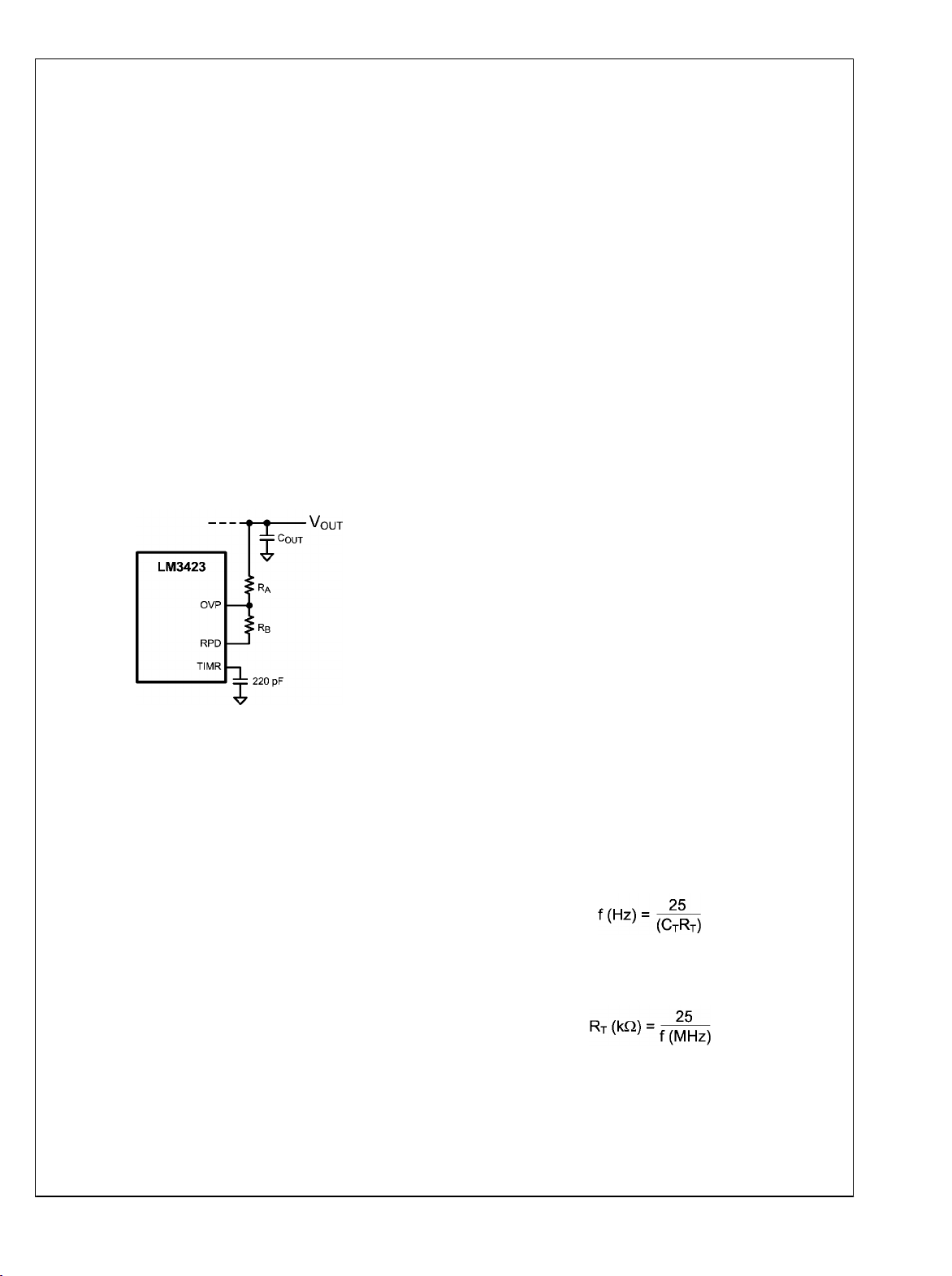
OVER-VOLTAGE PROTECTION
of the main power MOSFET can be used as the
DS(ON)
If the LEDs are referenced to a potential other than ground,
as in the VIN referenced flyback configuration, the output voltage (V
to use the OVLO function. This can be easily achieved using
) is best sensed and translated to ground in order
LED
a single PNP-type bipolar transistor as shown in Figure 4.
30067359
FIGURE 4. LED Forward Voltage OVP Sensing
Remember that the OVLO also protects the voltage on HSP
and HSN so the circuit in Figure 4 would not be appropriate
in cases where the total output voltage is greater than 75V
unless the sense resistor is imbedded within the LED string
at a voltage lower than 75V.
This OVLO feature can cause some interesting results if the
OVLO trip-point is set too close to the LED stack operating
voltage. At turn-on, the converter has a modest amount of
voltage overshoot before the control loop gains control of the
average current. If this overshoot exceeds the OVLO threshold, the controller shuts down, but in doing so it opens the
dimming MOSFET. This isolates the LED load from the converter and its output capacitors. With only the current flowing
into the HSP and HSN pins, the output voltage droops very
slowly and in approximately ½ second the output voltage
drops below the OVLO threshold and the converter turns back
on. An observer would see the LEDs blinking at about 2Hz.
This mode can often be escaped if the input voltage is reduced. This is because the maximum current limit on the IS
pin will limit the power intercepted by the converter at turn-on,
thus preventing any overshoot. A detailed description of the
turn-on overshoot and a simple solution are discussed in detail in the section titled STARTUP INRUSH CURRENT.
30067358
FIGURE 3. Over-Voltage Lock-Out Circuitry
The LM3421/LM3423 devices can be configured to detect either an input or an output over-voltage condition via the OVP
pin. The pin features a precision 1.24V threshold with 23µA
(typical) of hysteresis current. When the OVLO threshold is
exceeded, the over-voltage state is entered and the GATE pin
is immediately pulled low while the DDRV pin is pulled to the
LED off state to prevent damage to the LEDs. A current
source is turned on supplying 23µA of current out of the OVP
pin to allow a user programmed lower threshold of the OVP
hysteretic band (see Figure 3). To reduce the current consumption of the OVP voltage divider when in shutdown, the
lower resistor may be tied to the RPD pin.
www.national.com 12
OVER-CURRENT PROTECTION
The LM3421/LM3423 devices also feature over-current protection. Switching action is disabled whenever the current in
the LEDs is more than 30% above the regulation set point.
The dimming MOSFET switch driver (DDRV) is not disabled
however as this would immediately remove the fault condition
and cause oscillatory behavior.
THERMAL SHUTDOWN
Both devices include thermal shutdown. If the die temperature
reaches approximately 165°C the device will shut down until
it cools to a safe temperature at which point the device will
resume operation. If the adverse condition that is heating the
device is not removed, the device will continue to cycle on and
off to keep the die temperature below 165°C. Thermal shutdown has approximately 25°C of hysteresis. When in thermal
shutdown, both the main regulator MOSFET (GATE) and the
dimming MOSFET switch driver (DDRV) are disabled.
Page 13
LM3421, LM3423
LM3423 ONLY: FAULT TIMER AND STATUS FLAGS
Among the LM3423's additional pins are TIMR and FLT which
can be used in conjunction with an input disconnect MOSFET
switch will protect the module from various fault conditions.
An 11.5µA (typical) current is sourced from the TIMR pin
whenever any of the following conditions exist: (1) LED current is above regulation by more than 30% (over-current
protection has engaged as described above), (2) OVLO has
engaged, or (3) thermal limit protection has engaged. An external capacitor on the TIMR pin acts to program the fault filter
time. When the voltage on the TIMR pin reaches 1.24V, the
device is latched off and the N-channel MOSFET open drain
FLT pin transitions to a high impedance state. The TIMR pin
will be immediately pulled to ground (reset) if the fault condition is removed at any point during the filter period.
If immediate latching is desired, simply use a 220pF timing
cap on the TIMR pin. When using the EN and OVP pins in
conjunction with the RPD pull-down pin, a race condition exists when exiting the disabled (EN low) state. When disabled,
the OVP pin is pulled up to the output voltage because the
RPD pull-down is disabled, and this will appear to be a real
OVLO condition. The timer pin will immediately rise and latch
the controller to the fault state. To protect against this behavior, a minimum capacitor should be populated from the TIMR
pin to AGND of 220pF.
30067360
FIGURE 5. OVP Resistive Divider Grounded with RPD
If fault latching operation is not required, short the TIMR pin
to ground. Note that if the TIMR pin is shorted to ground, the
FLT flag function will also be disabled. When enabled, the FLT
pin can be used in conjunction with an external P-channel
MOSFET transistor to protect the module from shorts to
ground on the output, as shown in the full featured application
schematic (see Figure 15). A latched fault condition can be
cleared by pulling the EN pin low long enough for the VCC pin
to drop below 4.1V (approximately 200ms), forcing the TIMR
pin to ground, or by a complete power cycle.
The LM3423 also includes an LED Ready (LRDY) flag to notify the system that the LEDs are in proper regulation. The Nchannel MOSFET open drain LRDY pin is pulled low
whenever any of the following conditions are met: (1) V
UVLO has engaged, (2) LED current is below regulation by
more than 20%, (3) LED current is above regulation by more
than 30% (over-current protection has engaged), (4) overvoltage protection has engaged, (5) thermal limit protection
has engaged, or (6) the part has been latched off because of
a persistent fault condition. Note that the LRDY pin is pulled
low during startup of the device and remains low until the LED
current is in regulation.
CC
Application Information
PREDICTIVE OFF-TIME TOPOLOGY
A History Lesson
Any clocked peak current mode converter has a right half
plane zero when duty cycles exceed 50%, often referred to
as “current mode instability” or “sub-harmonic oscillation”. In
this context the word “clocked” should be considered to be a
free running oscillator that starts a new “on” cycle with each
tick. The right half plane zero manifests itself by a long ontime, short off-time cycle followed by a short on-time, long offtime cycle.
This instability leads to high stress in the components, creates
large voltage and current ripple at half of the clocked frequency, and often becomes audible. Slope compensation is usually introduced into the control system to prevent this
instability. As the required duty cycle approaches unity, the
amount of required slope compensation increases accordingly. Further complicating the problem, a boost converter
requires significantly more slope compensation than its buck
counterpart, thus becoming impractical for large voltage
transformation ratios. This translates to the necessity of limiting the maximum duty cycle in a boost converter and thus
the voltage transformation ratio.
History Learned is Not Repeated
The LM3421/LM3423 controllers feature a different constant
frequency control scheme, called predictive off-time control.
This topology has several innate advantages:
•
By not being clocked it has no current mode instability at
any duty cycle.
•
Allows duty cycles and thus voltage transformation ratios
that would be impractical in a clocked current mode
system, especially in a boost topology.
•
Requires no slope compensation.
The only disadvantage is that synchronization to an external
reference frequency is generally not available. Synchronization is “clocking” just like in an internal free running oscillator
and would reintroduce the right half plane zero unless it is
done with a phase locked loop.
SETTING THE SWITCHING FREQUENCY
For the boost, buck-boost, and SEPIC configurations, an external resistor connected between the RCT pin and the drain
of the main switching transistor, VSW, in combination with a
capacitor CT between the RCT and AGND pins, sets the
switching frequency. To set the operational frequency (f), the
RT resistor and CT capacitor can be calculated from:
We recommend a value of 1nF for CT and using that value,
this simplifies the equation to:
The RT resistor and CT capacitor should be located very close
to the device.
Buck Configuration
When the device is used to implement the buck topology the
control law is different. The internal circuitry of the device is
designed to run constant frequency in a boost, buck-boost or
13 www.national.com
Page 14

SEPIC application. When it is placed into a Buck converter a
current is set charging the RCT pin set up by the PNP transistor and resistor network (see Figure 13) the Off Time
T
is controlled to be:
OFF
LM3421, LM3423
This promotes a constant ripple converter were the ripple current magnitude is a function of the input voltage. There is no
output capacitor and the Dimming control MOSFET is shunting the current away from the LEDs. As the converter is
always in continuous conduction mode the duty factor is set
by the input and output voltages. This fact allows us to give
an equation for selecting the frequency setting components
for the Buck converter. To select a timing resistor use this
equation:
In the above equation RT is in kΩ, CT is in nF, and f is in MHz.
One could also select the timing resistor by setting their desired ripple current using the following equation:
For this equation RT is in kΩ, CT is in nF, L
I
is in A.
RIPPLE
The above describes a buck converter with constant ripple
regardless of V
LM3423 can also be set up in a buck configuration where the
ripple current varies with V
varying VIN. See Figure 14 for an example of how to imple-
but that varies with VIN. The LM3421/
LED
but remains constant over
LED
ment constant ripple vs. VIN.
INDUCTOR SELECTION
The inductor should be selected such that the switching regulator maintains continuous inductor current conduction over
the input and output operating voltage and current ranges.
The minimum inductor value is shown in the following equation for the non-Buck topologies:
CHOKE
is in µH, and
COMP pin. However, a two pole system results when an output capacitor is used to reduce the ripple current in the LEDs.
Two pole systems can become unstable because the total
phase shift approaches 180 degrees at unity gain crossover.
A zero in the control compensation is needed; this takes the
form of the resistor in series with the compensation capacitor.
The value of this resistor should be designed to provide the
same RC time constant with the compensation capacitor as
the output capacitor has with the dynamic impedance of the
LED string. If additional phase margin is desired, make the
compensation time constant slower than the output time constant (larger value of resistor).
FAST PWM DIMMING CAPABILITY
These devices provide fast PWM LED dimming, thus enabling
constant LED current for optimal color temperature. The
DDRV pin is meant to drive the gate of an external dimming
MOSFET. This drive will follow the PWM signal applied at the
nDIM pin. The active low nDIM pin can be driven with a PWM
signal up to 50kHz; the brightness of the LEDs can be varied
by modulating the duty cycle of this signal. LED brightness is
approximately proportional to the PWM signal duty cycle, so
30% duty cycle equals approximately 30% LED brightness.
This function can be ignored if PWM dimming is not required
by using nDIM solely as a VIN UVLO input or by tying it directly
to VCC or VIN (if less than 60VDC).
If high side dimming is implemented with a PMOS instead of
an NMOS, the polarity of the dimming MOSFET driver must
be reversed. The LM3423’s DPOL pin is used to set the polarity of the DIM driver output, DDRV. Tying DPOL to ground
causes the DDRV pin to be pulled up to VCC during dim operation, and should be used when driving a PMOS dimming
MOSFET. Note that when high side dimming, the high side
PMOS gate protection zener’s breakdown voltage should be
selected to be roughly equal to the VCC output voltage of approximately 7V. See Figure 16 for further information. Tying
DPOL to VCC or leaving it open causes the DDRV pin to be
low during dim operation and should be used when driving an
NMOS dimming MOSFET.
A minimum on-time must be maintained in order for PWM
dimming to operate in the linear region of its transfer function
(see the graphs Averege LED Current vs. PWM DIM Duty
Cycle and 30kHz PWM Dimming (5% Duty Cycle ON)). Be-
cause the controller is disabled during dimming, the PWM
pulse must be long enough such that the energy intercepted
from the input is greater than or equal to the energy being put
into the LEDs. For a boost and buck-boost regulator, the following condition must be maintained:
In the above equation K should be a value between 3 and 5
depending on the most important application requirements. A
lower value of K results in a smaller, lower cost inductor but
also in higher ripple and lower efficiency. A higher value of K
results in a larger, more costly inductor but will have lower
ripple and higher efficiency.
For the Buck topology the inductor value is selected for a desired ripple current as shown in the previous section.
COMPENSATION
The controllers’ error amplifier is a high output impedance,
transconductance amplifier for easy, single-pin compensation. This controller is a current mode controller and the
control loop feedback is monitoring the average output (LED)
current. As such it would be expected that the compensation
network could comprise a single capacitor to ground on the
www.national.com 14
In the previous equation, t
is seconds, I
peres, V
often referred to as V
henries, and VIN is the input voltage in volts.
is the average current in the LEDs in am-
LED
is the LED stack voltage in volts which is also
LED
OUT
is the length of the PWM pulse
PULSE
or V
, L in the inductance in
BOOST
BUCK HIGH SPEED DIMMING
These devices are able to implement a constant ripple buck
converter. In this mode the PWM control of LED dimming is
performed by shunting the current away from the LEDs and
through a MOSFET. Please refer to Figure 13 for the circuit
details.
Page 15

DETERMINING MAXIMUM NUMBER OF LEDS THAT CAN BE DRIVEN
The LM3421/LM3423 devices can drive any string of LEDs
that will allow the current sense resistor to be below 75V. The
sense resistor may be embedded within the string of LEDs to
allow driving a stack of LEDs whose highest potential is above
75V. In this configuration, the IS pin must be tied to a sourceside resistor; R
sensing is not an option.
DS(ON)
BOOST MODE INRUSH CURRENT
When configured as a boost converter, there is a “phantom”
power path comprised of the inductor, the output diode, and
the output capacitor. This path will cause two things to happen
when power is applied. First, there will be a very large inrush
of current to charge the output capacitor. Second, the energy
stored in the inductor during this inrush will end up in the output capacitor, charging it to a higher potential than the input
voltage. This voltage could, depending on the impedance of
the source, reach a peak value determined by the following
equation:
Depending on the state of the EN pin, the output capacitor
would be discharged by:
1) EN < 1.3V, no discharge path (leakage only).
2) EN > 1.3V, the OVP divider resistor path, if present, and
10µA into each of the HSP & HSN pins. This output capacitor
voltage could be higher than the OVP voltage. In this situation,
the FLT pin (LM3423 only) is open and the PWM dimming
MOSFET is turned off. This condition (the system appearing
disabled) can persist for an undesirably long time; possible
solutions include:
•
Add an inrush diode from VIN to the output. See Figure 6
•
Add an NTC thermistor to prevent the inrush from
overcharging the output capacitor so high.
•
A current limited source supply.
•
Raise the OVP threshold.
LM3421, LM3423
FIGURE 6. Boost Topology with Inrush Diode
STARTUP INRUSH CURRENT
The LM3421/LM3423 devices implement a true current
source; they regulate current into a string of LEDs. When an
output capacitor is used to reduce the ripple current into the
LEDs, it is outside of the current control loop. During startup,
an inrush current associated with charging the output capacitor up to the LED string “on” voltage is observed. During this
inrush, there is little or no current flow in the LEDs so the error
amplifier pulls the COMP pin up as high as it is able to. The
input current rapidly reaches the current limit value set by the
current limit comparator, 245mV (typical) across the main
power switch or its source resistor depending on how the IS
pin is configured. The input current stays “regulated” at that
30067362
point until the voltage on the output capacitor rises high
enough to drive current into the LED string. When the LED
string exceeds the programmed current, the control loop
forces the voltage on the COMP pin down until the output
current into the LEDs is in regulation. This takes time and results in an overshoot in the LED current as the loop settles to
its programmed value.
Regardless, this overshoot in LED current can, in some configurations, approach the 30% high over-current limit. As the
input voltage increases, the power intercepted from the input
source increases and therefore so does the associated overshoot. When the overshoot reaches 30%, the fault timer is
activated and a race starts between the control loop acting to
15 www.national.com
Page 16

bring the current down below the 30% high threshold and the
fault timer interval. For short timer intervals, the controller
simply shuts off in the fault lockdown mode. The user will observe the LEDs blink on once at power up should this condition exist. This overshoot of current can be prevented by
LM3421, LM3423
adding a control zero into the system as detailed in Figure 7.
Simply adding the shaded components eliminates this issue
(see Figure 8). Note that for many configurations these components will not be required.
I
= 1A nominal, VIN = 12V, V
LED
Top trace: EN input, 1V/div, DC
Bottom trace: I
T = 1ms/div
, 500mA/div, DC
LED
FIGURE 7. Boost LED Driver with Lead Compensation
= 20V, no lead compensation
LED(s)
30067372
I
= 1A nominal, VIN = 12V, V
LED
Top trace: EN input, 1V/div, DC
Bottom trace: I
T = 1ms/div
, 500mA/div, DC
LED
= 20V, with lead compensation
LED(s)
FIGURE 8. Scope Plots for Startup With and Without Lead Compensation
30067305
30067373
www.national.com 16
Page 17

LM3421, LM3423
Another method of limiting the turn on overshoot is the selection of the RIS Resistor that is between the IS pin and PGND.
If the MOSFET channel resistance is used there is little that
can be done, but by using a separate sense resistor placed
in the source of the Mosfet (Please refer to Figure 13 for circuit
details) the peak input current can be set. Setting the peak
current at the peak input voltage sets the peak power intercepted from the input during turn on. This sets the rate of rise
of voltage on the output capacitor, and consequently the
amount of overshoot seen as the control loop settles to its
programmed value.
SLOW SHUTDOWN FEATURE (FADE OUT)
In some applications, particularly automotive interior lighting,
it may be desirable for the LEDs to transition slowly to the off
state rather than abruptly shutting off. This can be easily accomplished with a few small and inexpensive external components, as show in Figure 9.
This circuit simply delays the shutdown on the EN pin and
slowly decreases the amount of current in the LEDs by decreasing the amount of current flowing out of the CSH pin,
which is directly proportional to the LED current as previously
discussed in the section titled PROGRAMMING AVERAGE
LED CURRENT.
DESIGN EXAMPLES
The following set of schematics show the LM3421/LM3423 in
various topology and feature set combinations. For more
complete schematics and associated Bills of Materials
(BoMs) and circuit board layouts, please see the application
notes associated with the various demonstration boards that
are available for these products.
30067361
FIGURE 9. LM3421/LM3423 Slow Shutdown Circuit
FIGURE 10. LM3421 Boost Topology with High Speed Dimming
30067331
17 www.national.com
Page 18

LM3421, LM3423
30067367
FIGURE 11. LM3421 Buck-Boost (Flyback) Topology with High Speed Dimming
FIGURE 12. LM3421 SEPIC Topology with High Speed Dimming
www.national.com 18
30067345
Page 19

30067368
LM3421, LM3423
FIGURE 13. LM3421 Buck Topology with High Speed Shunt PWM Dimming and Constant Ripple Current vs. V
LED
30067365
FIGURE 14. LM3421 Buck Topology with High Speed Shunt PWM Dimming and Constant Ripple Current vs. V
19 www.national.com
IN
Page 20

LM3421, LM3423
30067363
FIGURE 15. LM3423 Full Featured Application: Boost Topology, High Speed Dimming, Fault Detection, and Input
Disconnect Switch
30067364
FIGURE 16. LM3423 Boost Topology with High-Side Dimming
www.national.com 20
Page 21

Physical Dimensions inches (millimeters) unless otherwise noted
LM3421, LM3423
For Ordering, Refer to Ordering Information Table
For Ordering, Refer to Ordering Information Table
TSSOP-16 Pin EP Package (MXA)
NS Package Number MXA16A
TSSOP-20 Pin EP Package (MXA)
NS Package Number MXA20A
21 www.national.com
Page 22

Notes
For more National Semiconductor product information and proven design tools, visit the following Web sites at:
Products Design Support
Amplifiers www.national.com/amplifiers WEBENCH www.national.com/webench
Audio www.national.com/audio Analog University www.national.com/AU
Clock Conditioners www.national.com/timing App Notes www.national.com/appnotes
Data Converters www.national.com/adc Distributors www.national.com/contacts
Displays www.national.com/displays Green Compliance www.national.com/quality/green
Ethernet www.national.com/ethernet Packaging www.national.com/packaging
Interface www.national.com/interface Quality and Reliability www.national.com/quality
LVDS www.national.com/lvds Reference Designs www.national.com/refdesigns
Power Management www.national.com/power Feedback www.national.com/feedback
Switching Regulators www.national.com/switchers
LDOs www.national.com/ldo
LED Lighting www.national.com/led
PowerWise www.national.com/powerwise
Serial Digital Interface (SDI) www.national.com/sdi
Temperature Sensors www.national.com/tempsensors
Wireless (PLL/VCO) www.national.com/wireless
THE CONTENTS OF THIS DOCUMENT ARE PROVIDED IN CONNECTION WITH NATIONAL SEMICONDUCTOR CORPORATION
(“NATIONAL”) PRODUCTS. NATIONAL MAKES NO REPRESENTATIONS OR WARRANTIES WITH RESPECT TO THE ACCURACY
OR COMPLETENESS OF THE CONTENTS OF THIS PUBLICATION AND RESERVES THE RIGHT TO MAKE CHANGES TO
SPECIFICATIONS AND PRODUCT DESCRIPTIONS AT ANY TIME WITHOUT NOTICE. NO LICENSE, WHETHER EXPRESS,
IMPLIED, ARISING BY ESTOPPEL OR OTHERWISE, TO ANY INTELLECTUAL PROPERTY RIGHTS IS GRANTED BY THIS
DOCUMENT.
TESTING AND OTHER QUALITY CONTROLS ARE USED TO THE EXTENT NATIONAL DEEMS NECESSARY TO SUPPORT
NATIONAL’S PRODUCT WARRANTY. EXCEPT WHERE MANDATED BY GOVERNMENT REQUIREMENTS, TESTING OF ALL
PARAMETERS OF EACH PRODUCT IS NOT NECESSARILY PERFORMED. NATIONAL ASSUMES NO LIABILITY FOR
APPLICATIONS ASSISTANCE OR BUYER PRODUCT DESIGN. BUYERS ARE RESPONSIBLE FOR THEIR PRODUCTS AND
APPLICATIONS USING NATIONAL COMPONENTS. PRIOR TO USING OR DISTRIBUTING ANY PRODUCTS THAT INCLUDE
NATIONAL COMPONENTS, BUYERS SHOULD PROVIDE ADEQUATE DESIGN, TESTING AND OPERATING SAFEGUARDS.
EXCEPT AS PROVIDED IN NATIONAL’S TERMS AND CONDITIONS OF SALE FOR SUCH PRODUCTS, NATIONAL ASSUMES NO
LIABILITY WHATSOEVER, AND NATIONAL DISCLAIMS ANY EXPRESS OR IMPLIED WARRANTY RELATING TO THE SALE
AND/OR USE OF NATIONAL PRODUCTS INCLUDING LIABILITY OR WARRANTIES RELATING TO FITNESS FOR A PARTICULAR
PURPOSE, MERCHANTABILITY, OR INFRINGEMENT OF ANY PATENT, COPYRIGHT OR OTHER INTELLECTUAL PROPERTY
RIGHT.
LIFE SUPPORT POLICY
NATIONAL’S PRODUCTS ARE NOT AUTHORIZED FOR USE AS CRITICAL COMPONENTS IN LIFE SUPPORT DEVICES OR
LM3421, LM3423 N-Channel Controllers for Constant Current LED Drivers
SYSTEMS WITHOUT THE EXPRESS PRIOR WRITTEN APPROVAL OF THE CHIEF EXECUTIVE OFFICER AND GENERAL
COUNSEL OF NATIONAL SEMICONDUCTOR CORPORATION. As used herein:
Life support devices or systems are devices which (a) are intended for surgical implant into the body, or (b) support or sustain life and
whose failure to perform when properly used in accordance with instructions for use provided in the labeling can be reasonably expected
to result in a significant injury to the user. A critical component is any component in a life support device or system whose failure to perform
can be reasonably expected to cause the failure of the life support device or system or to affect its safety or effectiveness.
National Semiconductor and the National Semiconductor logo are registered trademarks of National Semiconductor Corporation. All other
brand or product names may be trademarks or registered trademarks of their respective holders.
Copyright© 2008 National Semiconductor Corporation
For the most current product information visit us at www.national.com
www.national.com
National Semiconductor
Americas Technical
Support Center
Email: support@nsc.com
Tel: 1-800-272-9959
National Semiconductor Europe
Technical Support Center
Email: europe.support@nsc.com
German Tel: +49 (0) 180 5010 771
English Tel: +44 (0) 870 850 4288
National Semiconductor Asia
Pacific Technical Support Center
Email: ap.support@nsc.com
National Semiconductor Japan
Technical Support Center
Email: jpn.feedback@nsc.com
 Loading...