

查询LM3420AM5X-8.2供应商
LM3420-4.2, -8.2, -8.4, -12.6, -16.8
Lithium-Ion Battery Charge Controller
LM3420-4.2, -8.2, -8.4, -12.6, -16.8 Lithium-Ion Battery Charge Controller
July 2000
General Description
The LM3420 series of controllers are monolithic integrated
circuits designed for charging and end-of-charge control for
Lithium-Ion rechargeable batteries. The LM3420 is available
in fivefixed voltage versions for one through four cell charger
applications (4.2V, 8.2V/8.4V, 12.6V and 16.8V respectively).
Included in a very small package is an (internally compensated) op amp, a bandgap reference, an NPN output transistor, and voltage setting resistors. The amplifier’s inverting input is externally accessible for loop frequency
compensation. The output is an open-emitter NPN transistor
capable of driving up to 15 mAof output current into external
circuitry.
A trimmed precision bandgap reference utilizes temperature
drift curvature correction for excellent voltage stability over
the operating temperature range. Available with an initial tolerance of 0.5% for the A grade version, and 1% for the standard version, the LM3420 allows for precision end-of-charge
control for Lithium-Ion rechargeable batteries.
The LM3420 is available in a sub-miniature 5-lead SOT23-5
surface mount package thus allowing very compact designs.
Features
n Voltage options for charging 1, 2, 3 or 4 cells
n Tiny SOT23-5 package
n Precision (0.5%) end-of-charge control
n Drive capability for external power stage
n Low quiescent current, 85 µA (typ.)
Applications
n Lithium-Ion battery charging
n Suitable for linear and switching regulator charger
designs
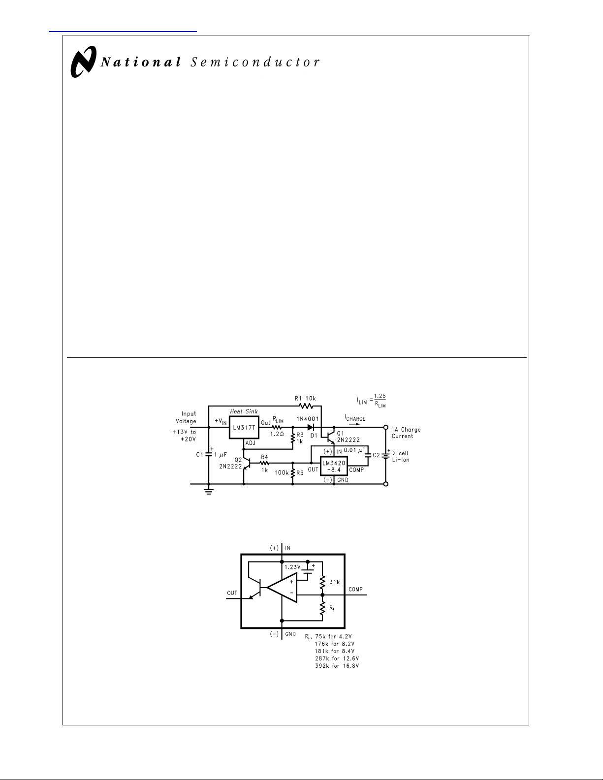
Typical Application and Functional Diagram
DS012359-1
Typical Constant Current/Constant Voltage
Li-Ion Battery Charger
DS012359-2
LM3420 Functional Diagram
SIMPLE SWITCHER®is a registered trademark of National Semiconductor Corporation.
© 2000 National Semiconductor Corporation DS012359 www.national.com
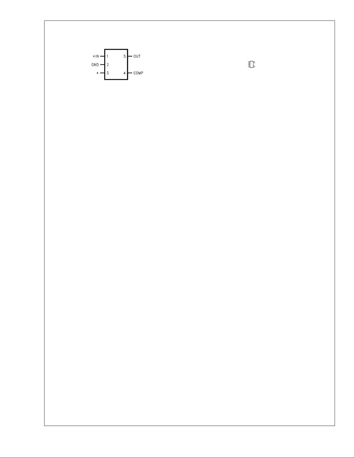
Connection Diagrams and Order Information
5-Lead Small Outline Package (M5)
DS012359-3
*No internal connection, but should be soldered to PC board for best heat
transfer.
Top View
For Ordering Information
See
Figure 1
See NS Package Number MF05A
LM3420-4.2/LM3420-8.2/LM3420-8.4/LM3420-12.6/LM3420-16.8
in this Data Sheet
Actual Size
DS012359-4
www.national.com 2
LM3420-4.2/LM3420-8.2/LM3420-8.4/LM3420-12.6/LM3420-16.8
Absolute Maximum Ratings (Note 1)
If Military/Aerospace specified devices are required,
please contact the National Semiconductor Sales Office/
Distributors for availability and specifications.
ESD Susceptibility (Note 3)
Human Body Model 1500V
See AN-450 “Surface Mounting Methods and Their Effect
on Product Reliability” for methods on soldering
surface-mount devices.
Input Voltage V(IN) 20V
Output Current 20 mA
Junction Temperature 150˚C
Storage Temperature −65˚C to +150˚C
Lead Temperature
Vapor Phase (60 seconds) +215˚C
Operating Ratings (Notes 1, 2)
Ambient Temperature Range −40˚C ≤ T
Junction Temperature Range −40˚C ≤ T
Output Current 15 mA
≤ +85˚C
A
≤ +125˚C
J
Infrared (15 seconds) +220˚C
Power Dissipation (T
(Note 2) 300 mW
= 25˚C)
A
LM3420-4.2
Electrical Characteristics
Specifications with standard type face are for TJ= 25˚C, and those with boldface type apply over full Operating Temperature Range. Unless otherwise specified, V(IN) = V
REG,VOUT
Symbol Parameter Conditions Typical LM3420A-4.2 LM3420-4.2 Units
V
REG
Regulation Voltage I
Regulation Voltage I
= 1 mA 4.2 V
OUT
=1mA
OUT
Tolerance
I
q
G
m
A
V
V
SAT
I
L
R
f
Quiescent Current I
Transconductance 20 µA ≤ I
∆I
/∆V
OUT
REG
Voltage Gain 1V ≤ V
∆V
/∆V
OUT
REG
Output Saturation V(IN) = V
(Note 7) I
Output Leakage V(IN) = V
Current V
= 1 mA 85 µA
OUT
≤ 1 mA 3.3 mA/mV
OUT
V
= 2V 1.3/0.75 1.0/0.50 mA/mV(min)
OUT
1mA≤I
V
OUT
≤ 15 mA 6.0 mA/mV
OUT
= 2V 3.0/1.5 2.5/1.4 mA/mV(min)
OUT
≤ V
− 1.2V (−1.3) 1000 V/V
REG
RL= 200Ω (Note 6) 550/250 450/200 V/V(min)
1V ≤ V
R
L
OUT
OUT
OUT
≤ V
− 1.2V (−1.3) 3500 V/V
REG
=2kΩ 1500/900 1000/700 V/V(min)
+100 mV 1.0 V
REG
= 15 mA 1.2/1.3 1.2/1.3 V(max)
−100 mV 0.1 µA
REG
= 0V 0.5/1.0 0.5/1.0 µA(max)
Internal Feedback 75 kΩ
Resistor (Note 8) 94 94 kΩ(max)
E
n
Output Noise I
= 1 mA, 10 Hz ≤ f ≤ 10 kHz 70 µV
OUT
Voltage
= 1.5V.
(Note 4) Limit Limit (Limits)
(Note 5) (Note 5)
4.221/4.242 4.242/4.284 V(max)
4.179/4.158 4.158/4.116 V(min)
±
0.5/±1
±1/±
2 %(max)
110/115 125/150 µA(max)
56 56 kΩ(min)
RMS
www.national.com3
LM3420-8.2
Electrical Characteristics
Specifications with standard type face are for TJ= 25˚C, and those with boldface type apply over full Operating Temperature Range. Unless otherwise specified, V(IN) = V
REG,VOUT
Symbol Parameter Conditions Typical LM3420A-8.2 LM3420-8.2 Units
V
REG
Regulation Voltage I
Regulation Voltage I
= 1 mA 8.2 V
OUT
=1mA
OUT
Tolerance
I
q
G
m
A
V
LM3420-4.2/LM3420-8.2/LM3420-8.4/LM3420-12.6/LM3420-16.8
V
SAT
I
L
R
f
Quiescent Current I
Transconductance 20 µA ≤ I
∆I
/∆V
OUT
REG
Voltage Gain 1V ≤ V
∆V
/∆V
OUT
REG
Output Saturation V(IN) = V
(Note 7) I
Output Leakage V(IN) = V
Current V
= 1 mA 85 µA
OUT
≤ 1 mA 3.3 mA/mV
OUT
V
= 6V 1.3/0.75 1.0/0.50 mA/mV(min)
OUT
1mA≤I
V
OUT
≤ 15 mA 6.0 mA/mV
OUT
= 6V 3.0/1.5 2.5/1.4 mA/mV(min)
OUT
≤ V
− 1.2V (−1.3) 1000 V/V
REG
RL= 470Ω (Note 6) 550/250 450/200 V/V(min)
1V ≤ V
R
=5kΩ 1500/900 1000/700 V/V(min)
L
OUT
OUT
OUT
≤ V
REG
− 1.2V (−1.3) 3500 V/V
REG
+100 mV 1.0 V
= 15 mA 1.2/1.3 1.2/1.3 V(max)
−100 mV 0.1 µA
REG
= 0V 0.5/1.0 0.5/1.0 µA(max)
Internal Feedback 176 kΩ
Resistor (Note 8) 220 220 kΩ(max)
E
n
Output Noise I
= 1 mA, 10 Hz ≤ f ≤ 10 kHz 140 µV
OUT
Voltage
= 1.5V.
(Note 4) Limit Limit (Limits)
(Note 5) (Note 5)
8.241/8.282 8.282/8.364 V(max)
8.159/8.118 8.118/8.036 V(min)
±
0.5/±1
±1/±
2 %(max)
110/115 125/150 µA(max)
132 132 kΩ(min)
RMS
LM3420-8.4
Electrical Characteristics
Specifications with standard type face are for TJ= 25˚C, and those with boldface type apply over full Operating Temperature Range. Unless otherwise specified, V(IN) = V
REG,VOUT
Symbol Parameter Conditions Typical LM3420A-8.4 LM3420-8.4 Units
V
REG
Regulation Voltage I
Regulation Voltage I
= 1 mA 8.4 V
OUT
=1mA
OUT
Tolerance
I
q
G
m
www.national.com 4
Quiescent Current I
= 1 mA 85 µA
OUT
Transconductance 20 µA ≤ I
∆I
OUT
/∆V
REG
V
= 6V 1.3/0.75 1.0/0.50 mA/mV(min)
OUT
1mA≤I
V
= 6V 3.0/1.5 2.5/1.4 mA/mV(min)
OUT
≤ 1 mA 3.3 mA/mV
OUT
≤ 15 mA 6.0 mA/mV
OUT
= 1.5V.
(Note 4) Limit Limit (Limits)
(Note 5) (Note 5)
8.442/8.484 8.484/8.568 V(max)
8.358/8.316 8.316/8.232 V(min)
±
0.5/±1
±1/±
2 %(max)
110/115 125/150 µA(max)
LM3420-8.4
Electrical Characteristics
Specifications with standard type face are for TJ= 25˚C, and those with boldface type apply over full Operating Temperature Range. Unless otherwise specified, V(IN) = V
Symbol Parameter Conditions Typical LM3420A-8.4 LM3420-8.4 Units
A
V
V
SAT
I
L
R
f
E
n
Voltage Gain 1V ≤ V
∆V
OUT
/∆V
REG
RL= 470Ω (Note 6) 550/250 450/200 V/V(min)
1V ≤ V
R
L
Output Saturation V(IN) = V
(Note 7) I
OUT
Output Leakage V(IN) = V
Current V
OUT
Internal Feedback 181 kΩ
Resistor (Note 8) 227 227 kΩ(max)
Output Noise I
OUT
Voltage
(Continued)
REG,VOUT
= 1.5V.
(Note 4) Limit Limit (Limits)
(Note 5) (Note 5)
OUT
OUT
≤ V
≤ V
− 1.2V (−1.3) 1000 V/V
REG
− 1.2V (−1.3) 3500 V/V
REG
=5kΩ 1500/900 1000/700 V/V(min)
+100 mV 1.0 V
REG
= 15 mA 1.2/1.3 1.2/1.3 V(max)
−100 mV 0.1 µA
REG
= 0V 0.5/1.0 0.5/1.0 µA(max)
135 135 kΩ(min)
= 1 mA, 10 Hz ≤ f ≤ 10 kHz 140 µV
RMS
LM3420-4.2/LM3420-8.2/LM3420-8.4/LM3420-12.6/LM3420-16.8
LM3420-12.6
Electrical Characteristics
Specifications with standard type face are for TJ= 25˚C, and those with boldface type apply over full Operating Temperature
Range. Unless otherwise specified, V(IN) = V
REG,VOUT
Symbol Parameter Conditions Typical LM3420A-12.6 LM3420-12.6 Units
V
REG
Regulation Voltage I
Regulation Voltage I
= 1 mA 12.6 V
OUT
=1mA
OUT
Tolerance
I
q
G
m
A
V
V
SAT
I
L
R
f
Quiescent Current I
Transconductance 20 µA ≤ I
∆I
/∆V
OUT
REG
Voltage Gain 1V ≤ V
∆V
/∆V
OUT
REG
Output Saturation V(IN) = V
(Note 7) I
Output Leakage V(IN) = V
Current V
= 1 mA 85 µA
OUT
≤ 1 mA 3.3 mA/mV
OUT
V
= 10V 1.3/0.75 1.0/0.5 mA/mV(min)
OUT
1mA≤I
V
OUT
≤ 15 mA 6.0 mA/mV
OUT
= 10V 3.0/1.5 2.5/1.4 mA/mV(min)
≤ V
OUT
REG
RL= 750Ω (Note 6) 550/250 450/200 V/V(min)
1V ≤ V
R
L
OUT
OUT
≤ V
OUT
REG
=10kΩ 1500/900 1000/700 V/V(min)
+100 mV 1.0 V
REG
= 15 mA 1.2/1.3 1.2/1.3 V(max)
−100 mV 0.1 µA
REG
= 0V 0.5/1.0 0.5/1.0 µA(max)
Internal Feedback 287 kΩ
Resistor (Note 8) 359 359 kΩ(max)
E
n
Output Noise
I
= 1 mA, 10 Hz ≤ f ≤ 10 kHz
OUT
Voltage
= 1.5V.
(Note 4) Limit Limit (Limits)
(Note 5) (Note 5)
12.663/12.726 12.726/12.852 V(max)
12.537/12.474 12.474/12.348 V(min)
±
0.5/±1
±1/±
2 %(max)
110/115 125/150 µA(max)
− 1.2V (−1.3) 1000 V/V
− 1.2V (−1.3) 3500 V/V
215 215 kΩ(min)
210 µV
RMS
www.national.com5
LM3420-16.8
Electrical Characteristics
Specifications with standard type face are for TJ= 25˚C, and those with boldface type apply over full Operating Temperature
Range. Unless otherwise specified, V(IN) = V
REG,VOUT
Symbol Parameter Conditions Typical LM3420A-16.8 LM3420-16.8 Units
V
REG
Regulation Voltage I
Regulation Voltage I
= 1 mA 16.8 V
OUT
=1mA
OUT
Tolerance
I
q
G
m
A
V
LM3420-4.2/LM3420-8.2/LM3420-8.4/LM3420-12.6/LM3420-16.8
V
SAT
I
L
R
f
Quiescent Current I
Transconductance 20 µA ≤ I
∆I
/∆V
OUT
REG
Voltage Gain 1V ≤ V
∆V
/∆V
OUT
REG
Output Saturation V(IN) = V
(Note 7) I
Output Leakage V(IN) = V
Current V
= 1 mA 85 µA
OUT
≤ 1 mA 3.3 mA/mV
OUT
V
= 15V 0.8/0.4 0.7/0.35 mA/mV(min)
OUT
1mA≤I
V
OUT
≤ 15 mA 6.0 mA/mV
OUT
= 15V 2.9/0.9 2.5/0.75 mA/mV(min)
≤ V
OUT
REG
RL=1kΩ(Note 6) 550/250 450/200 V/V(min)
1V ≤ V
R
L
OUT
OUT
≤ V
OUT
REG
=15kΩ 1200/750 1000/650 V/V(min)
+100 mV 1.0 V
REG
= 15 mA 1.2/1.3 1.2/1.3 V(max)
−100 mV 0.1 µA
REG
= 0V 0.5/1.0 0.5/1.0 µA(max)
Internal Feedback 392 kΩ
Resistor (Note 8) 490 490 kΩ(max)
E
n
Output Noise
I
= 1 mA, 10 Hz ≤ f ≤ 10 kHz
OUT
Voltage
Note 1: Absolute Maximum Ratings indicate limits beyond which damage to the device may occur. Operating Ratings indicate conditions for which the device is intended to be functional, but do not guarantee specific performance limits. For guaranteed specifications and test conditions, see the Electrical Characteristics. The
guaranteed specifications apply only for the test conditions listed. Some performance characteristics may degrade when the device is not operated under the listed
test conditions.
Note 2: The maximum power dissipation must be derated at elevated temperatures and is dictated by T
bient thermal resistance), and T
given in the Absolute Maximum Ratings, whichever is lower. The typical thermal resistance (θ
for the M5 package.
Note 3: The human body model is a 100 pF capacitor discharged through a 1.5 kΩ resistor into each pin.
Note 4: Typical numbers are at 25˚C and represent the most likely parametric norm.
Note 5: Limits are 100% production tested at 25˚C. Limits over the operating temperature range are guaranteed through correlation using Statistical Quality Control
(SQC) methods. The limits are used to calculate National’s Averaging Outgoing Quality Level (AOQL).
Note 6: Actual test is done using equivalent current sink instead of a resistor load.
Note 7: V
Note 8: See Applications and Typical Performance Characteristics sections for information on this resistor.
= V(IN) − V
SAT
(ambient temperature). The maximum allowable power dissipation at any temperature is P
A
, when the voltage at the IN pin is forced 100 mV above the nominal regulating voltage (V
OUT
= 1.5V.
(Note 4) Limit Limit (Limits)
(Note 5) (Note 5)
16.884/16.968 16.968/17.136 V(max)
16.716/16.632 16.632/16.464 V(min)
±
0.5/±1
±1/±
2 %(max)
110/115 125/150 µA(max)
− 1.2V (−1.3) 1000 V/V
− 1.2V (−1.3) 3500 V/V
294 294 kΩ(min)
280 µV
(maximum junction temperature), θJA(junction to am-
Jmax
) when soldered to a printed circuit board is approximately 306˚C/W
JA
REG
Dmax
).
=(T
Jmax−TA
)/θJAor the number
RMS
www.national.com 6
 Loading...