


April 8, 2008
LM3410
PowerWise® 525kHz/1.6MHz, Constant Current Boost and
SEPIC LED Driver with Internal Compensation
LM3410 PowerWise
Internal Compensation
General Description
The LM3410 constant current LED driver is a monolithic, high
frequency, PWM DC/DC converter in 5-pin SOT23, 6-pin LLP,
& 8-pin eMSOP packages. With a minimum of external components the LM3410 is easy to use. It can drive 2.8A typical
peak currents with an internal 170 mΩ NMOS switch. Switching frequency is internally set to either 525 kHz or 1.60 MHz,
allowing the use of extremely small surface mount inductors
and chip capacitors. Even though the operating frequency is
high, efficiencies up to 88% are easy to achieve. External
shutdown is included, featuring an ultra-low standby current
of 80 nA. The LM3410 utilizes current-mode control and internal compensation to provide high-performance over a wide
range of operating conditions. Additional features include
dimming, cycle-by-cycle current limit, and thermal shutdown.
Typical Boost Application Circuit
Features
Space Saving SOT23-5 & 6-LLP Package
■
Input voltage range of 2.7V to 5.5V
■
Output voltage range of 3V to 24V
■
2.8A Typical Switch Current
■
High Switching Frequency
■
525 KHz (LM3410-Y)
—
1.6 MHz (LM3410-X)
—
170 mΩ NMOS Switch
■
190 mV Internal Voltage Reference
■
Internal Soft-Start
■
Current-Mode, PWM Operation
■
Thermal Shutdown
■
Applications
LED Backlight Current Source
■
LiIon Backlight OLED & HB LED Driver
■
Handheld Devices
■
LED Flash Driver
■
®
525kHz/1.6MHz, Constant Current Boost and SEPIC LED Driver with
30038501
30038502
© 2008 National Semiconductor Corporation 300385 www.national.com

Connection Diagrams
LM3410
Top View
5–Pin SOT23
30038503
Top View
6-Pin LLP
Top View
30038504
8-Pin eMSOP
Ordering Information
Order Number Frequency Package Type Package Drawing Supplied As
LM3410YMF
LM3410YMFX 3000 units Tape & Reel
LM3410YMFE 250 units Tape & Reel
LM3410YSD
LM3410YSDX 4500 units Tape & Reel
LM3410YSDE 250 units Tape & Reel
LM3410YMY
LM3410YMYX 3500 units Tape & Reel
LM3410YMYE 250 units Tape & Reel
LM3410XMF
LM3410XMFX 3000 units Tape & Reel
LM3410XMFE 250 units Tape & Reel
LM3410XSD
LM3410XSDX 4500 units Tape & Reel
LM3410XSDE 250 units Tape & Reel
LM3410XMY
LM3410XMYX 3500 units Tape & Reel
LM3410XMYE 250 units Tape & Reel
525 kHz
1.6 MHz
SOT23-5 MF05A
LLP-6 SDE06A
eMSOP-8 MUY08A
SOT23-5 MF05A
LLP-6 SDE06A
eMSOP-8 MUY08A
1000 units Tape & Reel
1000 units Tape & Reel
1000 units Tape & Reel
1000 units Tape & Reel
1000 units tape & reel
1000 units Tape & Reel
30038505
www.national.com 2

Pin Descriptions - 5-Pin SOT23
Pin Name Function
1 SW Output switch. Connect to the inductor, output diode.
2 GND
3 FB Feedback pin. Connect FB to external resistor divider to set output voltage.
4 DIM
5 VIN Supply voltage pin for power stage, and input supply voltage.
Signal and power ground pin. Place the bottom resistor of the feedback network as close as possible to this
pin.
Dimming & shutdown control input. Logic high enables operation. Duty Cycle from 0 to 100%. Do not allow
this pin to float or be greater than VIN + 0.3V.
Pin Descriptions - 6-Pin LLP
Pin Name Function
1 PGND Power ground pin. Place PGND and output capacitor GND close together.
2 VIN Supply voltage for power stage, and input supply voltage.
3 DIM
4 FB Feedback pin. Connect FB to external resistor divider to set output voltage.
5 AGND
6 SW Output switch. Connect to the inductor, output diode.
DAP GND
Dimming & shutdown control input. Logic high enables operation. Duty Cycle from 0 to 100%. Do not allow
this pin to float or be greater than VIN + 0.3V.
Signal ground pin. Place the bottom resistor of the feedback network as close as possible to this pin & pin
4.
Signal & Power ground. Connect to pin 1 & pin 5 on top layer. Place 4-6 vias from DAP to bottom layer GND
plane.
LM3410
Pin Descriptions - 8-Pin eMSOP
Pin Name Function
1 - No Connect
2 PGND Power ground pin. Place PGND and output capacitor GND close together.
3 VIN Supply voltage for power stage, and input supply voltage.
4 DIM
5 FB Feedback pin. Connect FB to external resistor divider to set output voltage.
6 AGND Signal ground pin. Place the bottom resistor of the feedback network as close as possible to this pin & pin 5
7 SW Output switch. Connect to the inductor, output diode.
8 - No Connect
DAP GND
Dimming & shutdown control input. Logic high enables operation. Duty Cycle from 0 to 100%. Do not allow
this pin to float or be greater than VIN + 0.3V.
Signal & Power ground. Connect to pin 2 & pin 6 on top layer. Place 4-6 vias from DAP to bottom layer GND
plane.
3 www.national.com

Absolute Maximum Ratings (Note 1)
If Military/Aerospace specified devices are required,
LM3410
please contact the National Semiconductor Sales Office/
Distributors for availability and specifications.
V
IN
SW Voltage -0.5V to 26.5V
FB Voltage -0.5V to 3.0V
DIM Voltage -0.5V to 7.0V
ESD Susceptibility (Note 4)
Human Body Model 2kV
Junction Temperature (Note 2) 150°C
-0.5V to 7V
Storage Temp. Range -65°C to 150°C
Soldering Information
Infrared/Convection Reflow (15sec) 220°C
Operating Ratings (Note 1)
V
IN
V
(Note 5) 0V to V
DIM
V
SW
Junction Temperature Range -40°C to 125°C
Power Dissipation
(Internal) SOT23-5 400 mW
2.7V to 5.5V
3V to 24V
IN
Electrical Characteristics Limits in standard type are for T
= 25°C only; limits in boldface type apply over the
J
junction temperature (TJ) range of -40°C to 125°C. Minimum and Maximum limits are guaranteed through test, design, or statistical
correlation. Typical values represent the most likely parametric norm at TJ = 25°C, and are provided for reference purposes only.
VIN = 5V, unless otherwise indicated under the Conditions column.
Symbol Parameter Conditions Min Typ Max Units
V
FB
ΔVFB/V
I
FB
F
SW
D
MAX
D
MIN
R
DS(ON)
I
CL
Feedback Voltage 178 190 202 mV
Feedback Voltage Line Regulation
IN
VIN = 2.7V to 5.5V
- 0.06 - %/V
Feedback Input Bias Current - 0.1 1 µA
Switching Frequency
Maximum Duty Cycle
Minimum Duty Cycle
Switch On Resistance
LM3410-X 1200 1600 2000
LM3410-Y 360 525 680
LM3410-X 88 92 -
LM3410-Y 90 95 -
LM3410-X - 5 -
LM3410-Y - 2 -
SOT23-5 and eMSOP-8 - 170 330
LLP-6 190 350
Switch Current Limit 2.1 2.80 - A
kHz
%
%
mΩ
SU Start Up Time - 20 - µs
I
Q
Quiescent Current (switching)
Quiescent Current (shutdown)
UVLO Undervoltage Lockout
V
DIM_H
I
SW
I
DIM
Shutdown Threshold Voltage - - 0.4
Enable Threshold Voltage 1.8 - -
Switch Leakage
Dimming Pin Current Sink/Source - 100 - nA
LM3410-X VFB = 0.25
LM3410-Y VFB = 0.25
All Options V
DIM
= 0V
VIN Rising
VIN Falling
VSW = 24V
- 7.0 11
- 3.4 7
- 80 - nA
- 2.3 2.65
1.7 1.9 -
- 1.0 - µA
mA
V
V
www.national.com 4

Symbol Parameter Conditions Min Typ Max Units
θ
JA
θ
JC
T
SD
Note 1: Absolute Maximum Ratings indicate limits beyond which damage to the device may occur. Operating Ratings indicate conditions for which the device is
intended to be functional, but does not guarantee specific performance limits. For guaranteed specifications and conditions, see the Electrical Characteristics.
Note 2: Thermal shutdown will occur if the junction temperature exceeds the maximum junction temperature of the device.
Note 3: Applies for packages soldered directly onto a 3” x 3” PC board with 2oz. copper on 4 layers in still air.
Note 4: The human body model is a 100 pF capacitor discharged through a 1.5 kΩ resistor into each pin. Test method is per JESD22-A114.
Note 5: Do not allow this pin to float or be greater than VIN +0.3V.
Junction to Ambient
0 LFPM Air Flow (Note 3)
Junction to Case (Note 3)
Thermal Shutdown Temperature (Note 2) - 165 - °C
LLP-6 and eMSOP-8 Package - 80 -
SOT23-5 Package - 118 -
LLP-6 and eMSOP-8 Package - 18 -
SOT23-5 Package - 60 -
°C/W
°C/W
LM3410
5 www.national.com

Typical Performance Characteristics All curves taken at V
= 5.0V with configuration in typical
IN
application circuit shown in Application Information section of this datasheet. TJ = 25C, unless otherwise specified.
LM3410
LM3410-X Efficiency vs VIN (R
SET
= 4Ω)
LM3410-X Start-Up Signature
30038502
4 x 3.3V LEDs 500 Hz DIM FREQ D = 50%
30038508
Current Limit vs Temperature
DIM Freq & Duty Cycle vs Avg I-LED
R
vs Temperature
DSON
30038507
30038509
30038510
www.national.com 6
30038511

LM3410
Oscillator Frequency vs Temperature - "X"
30038512
VFB vs Temperature
Oscillator Frequency vs Temperature - "Y"
30038513
30038580
7 www.national.com

Simplified Internal Block Diagram
LM3410
FIGURE 1. Simplified Block Diagram
Application Information
THEORY OF OPERATION
The LM3410 is a constant frequency PWM, boost regulator
IC. It delivers a minimum of 2.1A peak switch current. The
device operates very similar to a voltage regulated boost converter except that it regulates the output current through
LEDs. The current magnitude is set with a series resistor. This
series resistor multiplied by the LED current creates the feedback voltage (190 mV) which the converter regulates to. The
regulator has a preset switching frequency of either 525 kHz
or 1.60 MHz. This high frequency allows the LM3410 to operate with small surface mount capacitors and inductors,
resulting in a DC/DC converter that requires a minimum
amount of board space. The LM3410 is internally compensated, so it is simple to use, and requires few external components. The LM3410 uses current-mode control to regulate
the LED current. The following operating description of the
LM3410 will refer to the Simplified Block Diagram (Figure 1)
the simplified schematic (Figure 2), and its associated waveforms (Figure 3). The LM3410 supplies a regulated LED
current by switching the internal NMOS control switch at constant frequency and variable duty cycle. A switching cycle
30038514
begins at the falling edge of the reset pulse generated by the
internal oscillator. When this pulse goes low, the output control logic turns on the internal NMOS control switch. During
this on-time, the SW pin voltage (VSW) decreases to approximately GND, and the inductor current (IL) increases with a
linear slope. IL is measured by the current sense amplifier,
which generates an output proportional to the switch current.
The sensed signal is summed with the regulator’s corrective
ramp and compared to the error amplifier’s output, which is
proportional to the difference between the feedback voltage
and V
output switch turns off until the next switching cycle begins.
During the switch off-time, inductor current discharges
through diode D1, which forces the SW pin to swing to the
output voltage plus the forward voltage (VD) of the diode. The
regulator loop adjusts the duty cycle (D) to maintain a regulated LED current.
. When the PWM comparator output goes high, the
REF
www.national.com 8

30038515
FIGURE 2. Simplified Boost Topology Schematic
LM3410
Design Guide
SETTING THE LED CURRENT
30038517
FIGURE 4. Setting I
LED
The LED current is set using the following equation:
where R
is connected between the FB pin and GND.
SET
DIM PIN / SHUTDOWN MODE
The average LED current can be controlled using a PWM
signal on the DIM pin. The duty cycle can be varied between
0 & 100% to either increase or decrease LED brightness.
PWM frequencies in the range of 1 Hz to 25 kHz can be used.
For controlling LED currents down to the µA levels, it is best
to use a PWM signal frequency between 200-1 kHz. The
maximum LED current would be achieved using a 100% duty
cycle, i.e. the DIM pin always high.
LED-DRIVE CAPABILITY
When using the LM3410 in the typical application configuration, with LEDs stacked in series between the VOUT and FB
pin, the maximum number of LEDs that can be placed in series is dependent on the maximum LED forward voltage
(VF
).
MAX
(VF
x N
MAX
When inserting a value for maximum VF
voltage variation over the operating temperature range
) + 190 mV < 24V
LEDs
the LED forward
MAX
should be considered.
30038516
FIGURE 3. Typical Waveforms
CURRENT LIMIT
The LM3410 uses cycle-by-cycle current limiting to protect
the internal NMOS switch. It is important to note that this current limit will not protect the output from excessive current
during an output short circuit. The input supply is connected
to the output by the series connection of an inductor and a
diode. If a short circuit is placed on the output, excessive current can damage both the inductor and diode.
THERMAL SHUTDOWN
Thermal shutdown limits total power dissipation by turning off
the output switch when the IC junction temperature exceeds
165°C. After thermal shutdown occurs, the output switch
doesn’t turn on until the junction temperature drops to approximately 150°C.
INDUCTOR SELECTION
The inductor value determines the input ripple current. Lower
inductor values decrease the physical size of the inductor, but
increase the input ripple current. An increase in the inductor
value will decrease the input ripple current.
9 www.national.com

LM3410
From the previous equations, the inductor value is then obtained.
30038519
FIGURE 5. Inductor Current
The Duty Cycle (D) for a Boost converter can be approximated by using the ratio of output voltage (V
(VIN).
) to input voltage
OUT
Therefore:
Power losses due to the diode (D1) forward voltage drop, the
voltage drop across the internal NMOS switch, the voltage
drop across the inductor resistance (R
losses must be included to calculate a more accurate duty
) and switching
DCR
cycle (See Calculating Efficiency and Junction Tempera-
ture for a detailed explanation). A more accurate formula for
calculating the conversion ratio is:
Where η equals the efficiency of the LM3410 application.
Or:
Therefore:
Where
1/TS = f
SW
One must also ensure that the minimum current limit (2.1A)
is not exceeded, so the peak current in the inductor must be
calculated. The peak current (Lpk I) in the inductor is calculated by:
I
= IIN + ΔIL or I
Lpk
Lpk
= I
OUT
/D' + Δi
L
When selecting an inductor, make sure that it is capable of
supporting the peak input current without saturating. Inductor
saturation will result in a sudden reduction in inductance and
prevent the regulator from operating correctly. Because of the
speed of the internal current limit, the peak current of the inductor need only be specified for the required maximum input
current. For example, if the designed maximum input current
is 1.5A and the peak current is 1.75A, then the inductor should
be specified with a saturation current limit of >1.75A. There is
no need to specify the saturation or peak current of the inductor at the 2.8A typical switch current limit.
Because of the operating frequency of the LM3410, ferrite
based inductors are preferred to minimize core losses. This
presents little restriction since the variety of ferrite-based inductors is huge. Lastly, inductors with lower series resistance
(DCR) will provide better operating efficiency. For recommended inductors see Example Circuits.
INPUT CAPACITOR
An input capacitor is necessary to ensure that VIN does not
drop excessively during switching transients. The primary
specifications of the input capacitor are capacitance, voltage,
RMS current rating, and ESL (Equivalent Series Inductance).
The recommended input capacitance is 2.2 µF to 22 µF depending on the application. The capacitor manufacturer
specifically states the input voltage rating. Make sure to check
any recommended deratings and also verify if there is any
significant change in capacitance at the operating input voltage and the operating temperature. The ESL of an input
capacitor is usually determined by the effective cross sectional area of the current path. At the operating frequencies
of the LM3410, certain capacitors may have an ESL so large
that the resulting impedance (2πfL) will be higher than that
required to provide stable operation. As a result, surface
mount capacitors are strongly recommended. Multilayer ceramic capacitors (MLCC) are good choices for both input and
output capacitors and have very low ESL. For MLCCs it is
recommended to use X7R or X5R dielectrics. Consult capacitor manufacturer datasheet to see how rated capacitance
varies over operating conditions.
Inductor ripple in a LED driver circuit can be greater than what
would normally be allowed in a voltage regulator Boost &
Sepic design. A good design practice is to allow the inductor
to produce 20% to 50% ripple of maximum load. The increased ripple shouldn’t be a problem when illuminating
LEDs.
www.national.com 10
OUTPUT CAPACITOR
The LM3410 operates at frequencies allowing the use of ceramic output capacitors without compromising transient response. Ceramic capacitors allow higher inductor ripple
without significantly increasing output ripple. The output capacitor is selected based upon the desired output ripple and
transient response. The initial current of a load transient is
provided mainly by the output capacitor. The output
impedance will therefore determine the maximum voltage
perturbation. The output ripple of the converter is a function

of the capacitor’s reactance and its equivalent series resistance (ESR):
When using MLCCs, the ESR is typically so low that the capacitive ripple may dominate. When this occurs, the output
ripple will be approximately sinusoidal and 90° phase shifted
from the switching action.
Given the availability and quality of MLCCs and the expected
output voltage of designs using the LM3410, there is really no
need to review any other capacitor technologies. Another
benefit of ceramic capacitors is their ability to bypass high
frequency noise. A certain amount of switching edge noise
will couple through parasitic capacitances in the inductor to
the output. A ceramic capacitor will bypass this noise while a
tantalum will not. Since the output capacitor is one of the two
external components that control the stability of the regulator
control loop, most applications will require a minimum at 0.47
µF of output capacitance. Like the input capacitor, recommended multilayer ceramic capacitors are X7R or X5R.
Again, verify actual capacitance at the desired operating voltage and temperature.
DIODE
The diode (D1) conducts during the switch off time. A Schottky
diode is recommended for its fast switching times and low
forward voltage drop. The diode should be chosen so that its
current rating is greater than:
ID1 ≥ I
OUT
The reverse breakdown rating of the diode must be at least
the maximum output voltage plus appropriate margin.
OUTPUT OVER-VOLTAGE PROTECTION
A simple circuit consisting of an external zener diode can be
implemented to protect the output and the LM3410 device
from an over-voltage fault condition. If an LED fails open, or
is connected backwards, an output open circuit condition will
occur. No current is conducted through the LED’s, and the
feedback node will equal zero volts. The LM3410 will react to
this fault by increasing the duty-cycle, thinking the LED current has dropped. A simple circuit that protects the LM3410
is shown in figure 6.
Zener diode D2 and resistor R3 is placed from V
with the string of LEDs. If the output voltage exceeds the
in parallel
OUT
breakdown voltage of the zener diode, current is drawn
through the zener diode, R3 and sense resistor R1. Once the
voltage across R1 and R3 equals the feedback voltage of
190mV, the LM3410 will limit its duty-cycle. No damage will
occur to the LM3410, the LED’s, or the zener diode. Once the
fault is corrected, the application will work as intended.
30038530
FIGURE 6. Overvoltage Protection Circuit
PCB Layout Considerations
When planning layout there are a few things to consider when
trying to achieve a clean, regulated output. The most important consideration when completing a Boost Converter layout
is the close coupling of the GND connections of the C
pacitor and the LM3410 PGND pin. The GND ends should be
close to one another and be connected to the GND plane with
at least two through-holes. There should be a continuous
ground plane on the bottom layer of a two-layer board except
under the switching node island. The FB pin is a high
impedance node and care should be taken to make the FB
trace short to avoid noise pickup and inaccurate regulation.
The R
possible to the IC, with the AGND of R
as possible to the AGND (pin 5 for the LLP) of the IC. Radiated
feedback resistor should be placed as close as
SET
(R1) placed as close
SET
noise can be decreased by choosing a shielded inductor. The
remaining components should also be placed as close as
possible to the IC. Please see Application Note AN-1229 for
further considerations and the LM3410 demo board as an example of a four-layer layout.
Below is an example of a good thermal & electrical PCB design.
30038532
OUT
ca-
LM3410
FIGURE 7. Boost PCB Layout Guidelines
This is very similar to our LM3410 demonstration boards that
are obtainable via the National Semiconductor website. The
demonstration board consists of a two layer PCB with a common input and output voltage application. Most of the routing
is on the top layer, with the bottom layer consisting of a large
ground plane. The placement of the external components
satisfies the electrical considerations, and the thermal perfor-
11 www.national.com

mance has been improved by adding thermal vias and a top
layer “Dog-Bone”.
LM3410
For certain high power applications, the PCB land may be
modified to a "dog bone" shape (see Figure 8). Increasing the
size of ground plane and adding thermal vias can reduce the
R
for the application.
θJA
30038533
FIGURE 8. PCB Dog Bone Layout
Thermal Design
When designing for thermal performance, one must consider
many variables:
Ambient Temperature: The surrounding maximum air temperature is fairly explanatory. As the temperature increases,
the junction temperature will increase. This may not be linear
though. As the surrounding air temperature increases, resistances of semiconductors, wires and traces increase. This will
decrease the efficiency of the application, and more power
will be converted into heat, and will increase the silicon junction temperatures further.
Forced Airflow: Forced air can drastically reduce the device
junction temperature. Air flow reduces the hot spots within a
design. Warm airflow is often much better than a lower ambient temperature with no airflow.
External Components: Choose components that are efficient, and you can reduce the mutual heating between devices.
PCB design with thermal performance in mind:
The PCB design is a very important step in the thermal design
procedure. The LM3410 is available in three package options
(5 pin SOT23, 8 pin eMSOP & 6 pin LLP). The options are
electrically the same, but difference between the packages is
size and thermal performance. The LLP and eMSOP have
thermal Die Attach Pads (DAP) attached to the bottom of the
packages, and are therefore capable of dissipating more heat
than the SOT23 package. It is important that the customer
choose the correct package for the application. A detailed
thermal design procedure has been included in this data
sheet. This procedure will help determine which package is
correct, and common applications will be analyzed.
There is one significant thermal PCB layout design consideration that contradicts a proper electrical PCB layout design
consideration. This contradiction is the placement of external
components that dissipate heat. The greatest external heat
contributor is the external Schottky diode. It would be nice if
you were able to separate by distance the LM3410 from the
Schottky diode, and thereby reducing the mutual heating effect. This will however create electrical performance issues.
It is important to keep the LM3410, the output capacitor, and
Schottky diode physically close to each other (see PCB layout
guidelines). The electrical design considerations outweigh the
thermal considerations. Other factors that influence thermal
performance are thermal vias, copper weight, and number of
board layers.
Thermal Definitions
Heat energy is transferred from regions of high temperature
to regions of low temperature via three basic mechanisms:
radiation, conduction and convection.
Radiation: Electromagnetic transfer of heat between masses
at different temperatures.
Conduction: Transfer of heat through a solid medium.
Convection: Transfer of heat through the medium of a fluid;
typically air.
Conduction & Convection will be the dominant heat transfer
mechanism in most applications.
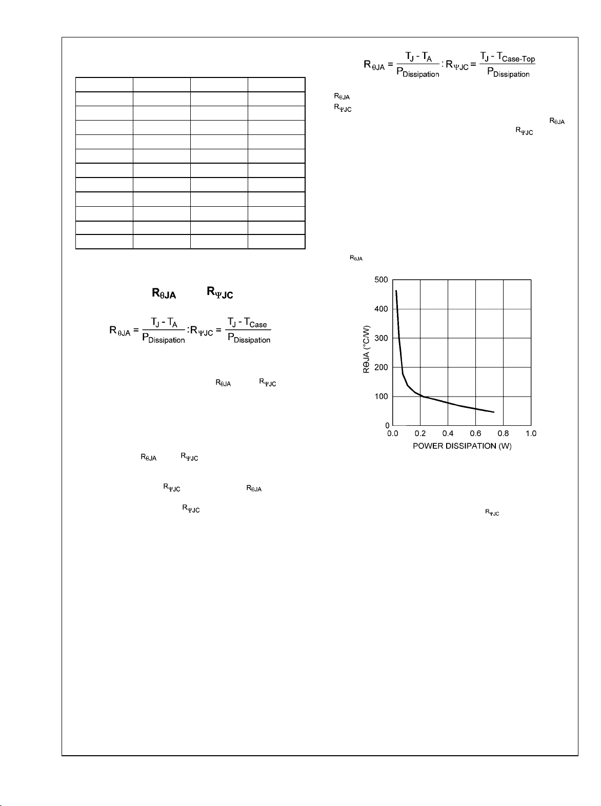
R
: Thermal impedance from silicon junction to ambient air
θJA
temperature.
R
: Thermal impedance from silicon junction to device case
θJC
temperature.
C
: Thermal Delay from silicon junction to device case tem-
θJC
perature.
C
: Thermal Delay from device case to ambient air tem-
θCA
perature.
R
& R
θJA
impedances, and most data sheets contain associated values
: These two symbols represent thermal
θJC
for these two symbols. The units of measurement are °C/
Watt.
R
is the sum of smaller thermal impedances (see simplified
θJA
thermal model Figures 9 and 10). Capacitors within the model
represent delays that are present from the time that power
and its associated heat is increased or decreased from steady
state in one medium until the time that the heat increase or
decrease reaches steady state in the another medium.
The datasheet values for these symbols are given so that one
might compare the thermal performance of one package
against another. To achieve a comparison between packages, all other variables must be held constant in the comparison (PCB size, copper weight, thermal vias, power
dissipation, VIN, V
on the package performance, but it would be a mistake to use
, load current etc). This does shed light
OUT
these values to calculate the actual junction temperature in
your application.
LM3410 Thermal Models
Heat is dissipated from the LM3410 and other devices. The
external loss elements include the Schottky diode, inductor,
and loads. All loss elements will mutually increase the heat
on the PCB, and therefore increase each other’s temperatures.
www.national.com 12

FIGURE 9. Thermal Schematic
LM3410
30038534
FIGURE 10. Associated Thermal Model
13 www.national.com
30038535
Calculating Efficiency, and Junction Temperature
LM3410
We will talk more about calculating proper junction temperature with relative certainty in a moment. For now we need to
describe how to calculate the junction temperature and clarify
some common misconceptions.
A common error when calculating R
package is the only variable to consider.
R
[variables]:
θJA
•
Input Voltage, Output Voltage, Output Current, R
•
Ambient temperature & air flow
•
Internal & External components power dissipation
•
Package thermal limitations
•
PCB variables (copper weight, thermal via’s, layers
component placement)
Another common error when calculating junction temperature
is to assume that the top case temperature is the proper temperature when calculating R
impedance of all six sides of a package, not just the top side.
θJC
This document will refer to a thermal impedance called
represents a thermal impedance associated with just the
top case temperature. This will allow one to calculate the
junction temperature with a thermal sensor connected to the
top case.
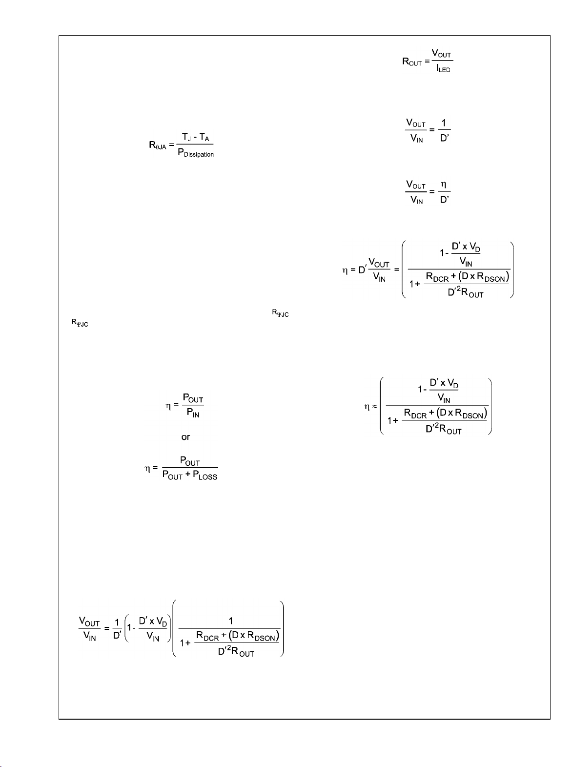
The complete LM3410 Boost converter efficiency can be calculated in the following manner.
is to assume that the
θJA
. R
represents the thermal
θJC
DS(ON)
One can see that if the loss elements are reduced to zero, the
conversion ratio simplifies to:
And we know:
Therefore:
.
Calculations for determining the most significant power losses are discussed below. Other losses totaling less than 2%
are not discussed.
A simple efficiency calculation that takes into account the
conduction losses is shown below:
Power loss (P
converter, switching and conduction. Conduction losses usu-
) is the sum of two types of losses in the
LOSS
ally dominate at higher output loads, where as switching
losses remain relatively fixed and dominate at lower output
loads.
Losses in the LM3410 Device: P
LOSS
= P
COND
+ PSW + P
Q
Where PQ = quiescent operating power loss
Conversion ratio of the Boost Converter with conduction loss
elements inserted:
Where
R
= Inductor series resistance
DCR
www.national.com 14
The diode, NMOS switch, and inductor DCR losses are included in this calculation. Setting any loss element to zero will
simplify the equation.
VD is the forward voltage drop across the Schottky diode. It
can be obtained from the manufacturer’s Electrical Characteristics section of the data sheet.
The conduction losses in the diode are calculated as follows:
P
= VD x I
DIODE
LED
Depending on the duty cycle, this can be the single most significant power loss in the circuit. Care should be taken to
choose a diode that has a low forward voltage drop. Another
concern with diode selection is reverse leakage current. Depending on the ambient temperature and the reverse voltage
across the diode, the current being drawn from the output to
the NMOS switch during time D could be significant, this may
increase losses internal to the LM3410 and reduce the overall
efficiency of the application. Refer to Schottky diode
manufacturer’s data sheets for reverse leakage specifications, and typical applications within this data sheet for diode
selections.
Another significant external power loss is the conduction loss
in the input inductor. The power loss within the inductor can
be simplified to:

2
= I
R
DCR
IN
P
IND
or
The LM3410 conduction loss is mainly associated with the
internal power switch:
P
COND-NFET
= I
2
SW-rms
x R
DSON
x D
30038542
FIGURE 11. LM3410 Switch Current
(small ripple approximation)
P
COND-NFET
= I
x R
IN
DSON
x D
2
or
The value for R
junction temperature you wish to analyze. As an example, at
125°C and R
should be equal to the resistance at the
DSON
= 250 mΩ (See typical graphs for value).
DSON
Switching losses are also associated with the internal power
switch. They occur during the switch on and off transition periods, where voltages and currents overlap resulting in power
loss.
The simplest means to determine this loss is to empirically
measuring the rise and fall times (10% to 90%) of the switch
at the switch node:
P
P
SWR
SWF
= 1/2(V
= 1/2(V
PSW = P
x IIN x fSW x t
OUT
x IIN x fSW x t
OUT
+ P
SWR
SWF
RISE
FALL
)
)
Typical Switch-Node Rise and Fall Times
V
IN
V
OUT
t
RISE
t
FALL
3V 5V 6nS 4nS
5V 12V 6nS 5nS
3V 12V 8nS 7nS
5V 18V 10nS 8nS
Quiescent Power Losses
IQ is the quiescent operating current, and is typically around
1.5 mA.
R
Power Loss
SET
PQ = IQ x V
IN
Example Efficiency Calculation:
Operating Conditions:
5 x 3.3V LEDs + 190mV
TABLE 1. Operating Conditions
V
IN
V
OUT
I
LED
V
D
f
SW
I
Q
t
RISE
t
FALL
R
DSON
L
DCR
D 0.82
I
IN
ΣP
+ PSW + P
COND
Quiescent Power Loss:
PQ = IQ x VIN = 10 mW
Switching Power Loss:
P
= 1/2(V
SWR
P
= 1/2(V
SWF
PSW = P
Internal NFET Power Loss:
P
CONDUCTION
Diode Loss:
VD = 0.45V
P
DIODE
Inductor Power Loss:
R
= 75 mΩ
DCR
P
IND
≊ 16.7V
REF
DIODE
x IIN x fSW x t
OUT
x IIN x fSW x t
OUT
+ P
SWR
R
= 225 mΩ
DSON
2
x D x R
= I
IN
IIN = 310 mA
= VD x I
2
x R
= I
IN
+ P
= 80 mW
SWF
= 23 mW
LED
= 7 mW
DCR
+ PQ = P
IND
RISE
FALL
DSON
3.3V
16.7V
50mA
0.45V
1.60MHz
3mA
10nS
10nS
225mΩ
75mΩ
0.31A
LOSS
) ≊ 40 mW
) ≊ 40 mW
= 17 mW
LM3410
15 www.national.com
Total Power Losses are:
LM3410
TABLE 2. Power Loss Tabulation
V
t
R
L
V
IN
OUT
I
LED
V
f
SW
I
Q
RISE
I
Q
DSON
DCR
D
3.3V
16.7V
50mA P
0.45V P
1.6MHz
10nS P
10nS P
3mA P
225mΩ
75mΩ
DIODE
P
COND
P
OUT
SWR
SWF
Q
IND
D 0.82
η
85% P
LOSS
P
INTERNAL
= P
+ PSW = 107 mW
COND
Calculating and
We now know the internal power dissipation, and we are trying to keep the junction temperature at or below 125°C. The
next step is to calculate the value for and/or . This is
actually very simple to accomplish, and necessary if you think
you may be marginal with regards to thermals or determining
what package option is correct.
The LM3410 has a thermal shutdown comparator. When the
silicon reaches a temperature of 165°C, the device shuts
down until the temperature drops to 150°C. Knowing this, one
can calculate the or the of a specific application. Because the junction to top case thermal impedance is much
lower than the thermal impedance of junction to ambient air,
the error in calculating is lower than for . However,
you will need to attach a small thermocouple onto the top case
of the LM3410 to obtain the value.
Knowing the temperature of the silicon when the device shuts
down allows us to know three of the four variables. Once we
calculate the thermal impedance, we then can work backwards with the junction temperature set to 125°C to see what
maximum ambient air temperature keeps the silicon below
the 125°C temperature.
Procedure:
Place your application into a thermal chamber. You will need
to dissipate enough power in the device so you can obtain a
good thermal impedance value.
Raise the ambient air temperature until the device goes into
thermal shutdown. Record the temperatures of the ambient
air and/or the top case temperature of the LM3410. Calculate
the thermal impedances.
Example from previous calculations (SOT23-5 Package):
P
TA @ Shutdown = 155°C
TC @ Shutdown = 159°C
INTERNAL
= 107 mW
825W
23mW
40mW
40mW
10mW
17mW
7mW
137mW
SOT23-5 = 93°C/W
SOT23-5 = 56°C/W
Typical LLP & eMSOP typical applications will produce
numbers in the range of 50°C/W to 65°C/W, and will vary
between 18°C/W and 28°C/W. These values are for PCB’s
with two and four layer boards with 0.5 oz copper, and four to
six thermal vias to bottom side ground plane under the DAP.
The thermal impedances calculated above are higher due to
the small amount of power being dissipated within the device.
Note: To use these procedures it is important to dissipate an
amount of power within the device that will indicate a true
thermal impedance value. If one uses a very small internal
dissipated value, one can see that the thermal impedance
calculated is abnormally high, and subject to error. Figure 12
shows the nonlinear relationship of internal power dissipation
vs .
.
30038551
FIGURE 12. R
For 5-pin SOT23 package typical applications, R
will range from 80°C/W to 110°C/W, and will vary between
vs Internal Dissipation
θJA
numbers
θJA
50°C/W and 65°C/W. These values are for PCB’s with two &
four layer boards with 0.5 oz copper, with two to four thermal
vias from GND pin to bottom layer.
Here is a good rule of thumb for typical thermal impedances,
and an ambient temperature maximum of 75°C: If your design
requires that you dissipate more than 400mW internal to the
LM3410, or there is 750mW of total power loss in the application, it is recommended that you use the 6 pin LLP or the 8
pin eMSOP package with the exposed DAP.
SEPIC Converter
The LM3410 can easily be converted into a SEPIC converter.
A SEPIC converter has the ability to regulate an output voltage that is either larger or smaller in magnitude than the input
voltage. Other converters have this ability as well (CUK and
Buck-Boost), but usually create an output voltage that is opposite in polarity to the input voltage. This topology is a perfect
fit for Lithium Ion battery applications where the input voltage
for a single cell Li-Ion battery will vary between 2.7V & 4.5V
and the output voltage is somewhere in between. Most of the
www.national.com 16
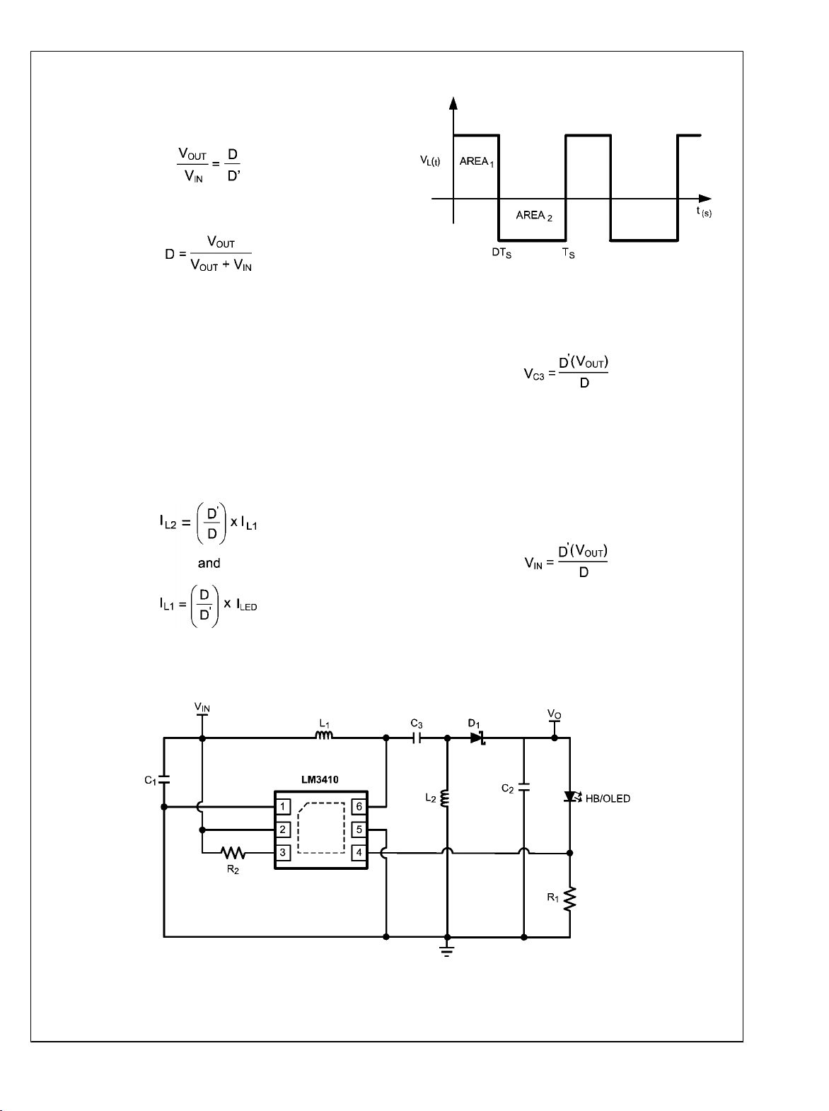
LM3410
analysis of the LM3410 Boost Converter is applicable to the
LM3410 SEPIC Converter.
SEPIC Design Guide:
SEPIC Conversion ratio without loss elements:
Therefore:
Small ripple approximation:
In a well-designed SEPIC converter, the output voltage, and
input voltage ripple, the inductor ripple IL1 and IL2 is small in
comparison to the DC magnitude. Therefore it is a safe approximation to assume a DC value for these components. The
main objective of the Steady State Analysis is to determine
the steady state duty-cycle, voltage and current stresses on
all components, and proper values for all components.
In a steady-state converter, the net volt-seconds across an
inductor after one cycle will equal zero. Also, the charge into
a capacitor will equal the charge out of a capacitor in one cycle.
Therefore:
The average inductor current of L2 is the average output load.
30038556
FIGURE 13. Inductor Volt-Sec Balance Waveform
Applying Charge balance on C1:
Since there are no DC voltages across either inductor, and
capacitor C3 is connected to Vin through L1 at one end, or to
ground through L2 on the other end, we can say that
VC3 = V
IN
Therefore:
Substituting IL1 into I
This verifies the original conversion ratio equation.
It is important to remember that the internal switch current is
equal to IL1 and IL2 during the D interval. Design the converter
L2
IL2 = I
LED
so that the minimum guaranteed peak switch current limit
(2.1A) is not exceeded.
30038552
FIGURE 14. HB/OLED SEPIC CONVERTER Schematic
17 www.national.com

Steady State Analysis with Loss Elements
LM3410
30038559
FIGURE 15. SEPIC Simplified Schematic
Using inductor volt-second balance & capacitor charge balance, the following equations are derived:
IL2 = (I
LED
)
and
IL1 = (I
) x (D/D')
LED
Therefore:
One can see that all variables are known except for the duty
cycle (D). A quadratic equation is needed to solve for D. A
less accurate method of determining the duty cycle is to assume efficiency, and calculate the duty cycle.
TABLE 3. Efficiencies for Typical SEPIC Applications
V
V
OUT
I
IN
I
LED
η
IN
2.7V V
3.1V V
770mA I
500mA I
75%
IN
OUT
IN
LED
η
3.3V V
3.1V V
600mA I
500mA I
80%
OUT
IN
LED
η
IN
5V
3.1V
375mA
500mA
83%
SEPIC Converter PCB Layout
The layout guidelines described for the LM3410 Boost-Converter are applicable to the SEPIC OLED Converter. Figure
16 is a proper PCB layout for a SEPIC Converter.
www.national.com 18
30038565
FIGURE 16. HB/OLED SEPIC PCB Layout

LM3410X SOT23-5 Design Example 1: 5 x 1206 Series LED String Application
LM3410
LM3410X (1.6MHz): VIN = 2.7V to 5.5V, 5 x 3.3V LEDs, (V
Part ID Part Value Manufacturer Part Number
U1 2.8A ISW LED Driver NSC LM3410XMF
C1, Input Cap 10µF, 6.3V, X5R TDK C2012X5R0J106M
C2 Output Cap 2.2µF, 25V, X5R TDK C2012X5R1E225M
D1, Catch Diode 0.4Vf Schottky 500mA, 30V
L1 10µH 1.2A Coilcraft DO1608C-103
R1
R2
LED's
SMD-1206, 50mA, Vf ≊ 3 .6V
4.02Ω, 1%
100kΩ, 1%
R
Diodes Inc MBR0530
≊ 16.5V) I
OUT
Vishay CRCW08054R02F
Vishay CRCW08051003F
Lite-On LTW-150k
≊ 50mA
LED
30038581
19 www.national.com

LM3410Y SOT23-5 Design Example 2: 5 x 1206 Series LED String Application
LM3410
LM3410Y (550kHz): VIN = 2.7V to 5.5V, 5 x 3.3V LEDs, (V
Part ID Part Value Manufacturer Part Number
U1 2.8A ISW LED Driver NSC LM3410YMF
C1, Input Cap 10µF, 6.3V, X5R TDK C2012X5R0J106M
C2 Output Cap 2.2µF, 25V, X5R TDK C2012X5R1E225M
D1, Catch Diode 0.4Vf Schottky 500mA, 30V
L1 15µH 1.2A Coilcraft DO1608C-153
R1
R2
LED's
SMD-1206, 50mA, Vf ≊ 3 .6V
4.02Ω, 1%
100kΩ, 1%
R
Diodes Inc MBR0530
≊ 16.5V) I
OUT
Vishay CRCW08054R02F
Vishay CRCW08051003F
Lite-On LTW-150k
≊ 50mA
LED
30038581
www.national.com 20

LM3410X LLP-6 Design Example 3: 7 LEDs x 5 LED String Backlighting Application
LM3410
LM3410X (1.6MHz): VIN = 2.7V to 5.5V, 7 x 5 x 3.3V LEDs, (V
Part ID Part Value Manufacturer Part Number
U1 2.8A ISW LED Driver NSC LM3410XSD
C1, Input Cap 10µF, 6.3V, X5R TDK C2012X5R0J106M
C2 Output Cap 4.7µF, 25V, X5R TDK C2012X5R1E475M
D1, Catch Diode 0.4Vf Schottky 500mA, 30V
L1 8.2µH, 2A Coilcraft MSS6132-822ML
R1
R2
LED's
SMD-1206, 50mA, Vf ≊ 3 .6V
1.15Ω, 1%
100kΩ, 1%
R
Diodes Inc MBR0530
Vishay CRCW08051R15F
Vishay CRCW08051003F
Lite-On LTW-150k
≊ 16.7V), I
OUT
≊ 25mA
LED
300385a2
21 www.national.com

LM3410X LLP-6 Design Example 4: 3 x HB LED String Application
LM3410
LM3410X (1.6MHz): VIN = 2.7V to 5.5V, 3 x 3.4V LEDs, (V
Part ID Part Value Manufacturer Part Number
U1 2.8A ISW LED Driver NSC LM3410XSD
C1, Input Cap 10µF, 6.3V, X5R TDK C2012X5R0J106M
C2 Output Cap 2.2µF, 25V, X5R TDK C2012X5R1E225M
D1, Catch Diode 0.4Vf Schottky 500mA, 30V
L1 10µH 1.2A Coilcraft DO1608C-103
R1
R2
R3
HB - LED's
1.00Ω, 1%
100kΩ, 1%
1.50Ω, 1%
340mA, Vf ≊ 3 .6V
R
Diodes Inc MBR0530
≊ 11V) I
OUT
Vishay CRCW08051R00F
Vishay CRCW08051003F
Vishay CRCW08051R50F
CREE XREWHT-L1-0000-0901
≊ 340mA
LED
30038567
www.national.com 22

LM3410Y SOT23-5 Design Example 5: 5 x 1206 Series LED String Application with OVP
LM3410
LM3410Y (525kHz): VIN = 2.7V to 5.5V, 5 x 3.3V LEDs, (V
Part ID Part Value Manufacturer Part Number
U1 2.8A ISW LED Driver NSC LM3410YMF
C1 Input Cap 10µF, 6.3V, X5R TDK C2012X5R0J106M
C2 Output Cap 2.2µF, 25V, X5R TDK C2012X5R1E225M
D1, Catch Diode 0.4Vf Schottky 500mA, Diodes Inc MBR0530
D2 18V Zener diode Diodes Inc 1N4746A
L1 15µH, 0.70A TDK VLS4012T-150MR65
R1
R2
R3
LED’s
SMD-1206, 50mA, Vf ≊ 3 .6V
4.02Ω, 1%
100kΩ, 1%
100kΩ, 1%
≊ 16.5V) I
OUT
Vishay CRCW08054R02F
Vishay CRCW08051003F
Vishay CRCW06031000F
Lite-On LTW-150k
≊ 50mA
LED
30038568
23 www.national.com

LM3410X SEPIC LLP-6 Design Example 6: HB/OLED Illumination Application
LM3410
LM3410X (1.6MHz): VIN = 2.7V to 5.5V, (V
Part ID Part Value Manufacturer Part Number
U1 2.8A ISW LED Driver NSC LM3410XSD
C1 Input Cap 10µF, 6.3V, X5R TDK C2012X5R0J106K
C2 Output Cap 10µF, 6.3V, X5R TDK C2012X5R0J106K
C3 Cap 2.2µF, 25V, X5R TDK C2012X5R1E225M
D1, Catch Diode 0.4Vf, Schottky 1A, 20V
L1 & L2 4.7µH 3A Coilcraft MSS6132-472
R1
R2
HB - LED’s
665 mΩ, 1%
100kΩ, 1%
350mA, Vf ≊ 3 .6V
R
≊ 3.8V) I
OUT
Diodes Inc DFLS120L
Vishay CRCW0805R665F
Vishay CRCW08051003F
CREE XREWHT-L1-0000-0901
≊ 300mA
LED
30038552
www.national.com 24

LM3410X LLP-6 Design Example 7: Boost Flash Application
LM3410
LM3410X (1.6MHz): VIN = 2.7V to 5.5V, (V
OUT
≊ 8V) I
≊ 1.0A Pulsed
LED
30038570
Part ID Part Value Manufacturer Part Number
U1 2.8A ISW LED Driver NSC LM3410XSD
C1 Input Cap 10µF, 6.3V, X5R TDK C2012X5R0J106M
C2 Output Cap 10µF,16V, X5R TDK C2012X5R1A106M
D1, Catch Diode 0.4Vf Schottky 500mA, 30V
R
Diodes Inc MBR0530
L1 4.7µH, 3A Coilcraft MSS6132-472
R1
LED’s
200mΩ, 1%
500mA, Vf ≊ 3 .6V, I
PULSE
= 1.0A
Vishay CRCW0805R200F
CREE XREWHT-L1-0000-0901
25 www.national.com

LM3410X SOT23-5 Design Example 8: 5 x 1206 Series LED String Application with VIN > 5.5V
LM3410
LM3410X (1.6MHz): V
= 9V to 14V, (V
PWR
≊ 16.5V) I
OUT
≊ 50mA
LED
30038571
Part ID Part Value Mfg Part Number
U1 2.8A ISW LED Driver NSC LM3410XMF
C1 Input V
Cap 10µF, 6.3V, X5R TDK C2012X5R0J106M
PWR
C2 Output Cap 2.2µF, 25V, X5R TDK C2012X5R1E225M
C2 Input VIN Cap 0.1µF, 6.3V, X5R TDK C1005X5R1C104K
D1, Catch Diode 0.43Vf, Schotky, 0.5A, 30V
R
Diodes Inc MBR0530
L1 10µH 1.2A Coilcraft DO1608C-103
R1
R2
R3
4.02Ω, 1%
100kΩ, 1%
576Ω, 1%
Vishay CRCW08054R02F
Vishay CRCW08051003F
Vishay CRCW08055760F
D2 3.3V Zener, SOT23 Diodes Inc BZX84C3V3
LED’s
SMD-1206, 50mA, Vf ≊ 3 .6V
Lite-On LTW-150k
www.national.com 26

LM3410X LLP-6 Design Example 9: Camera Flash or Strobe Circuit Application
LM3410
LM3410X (1.6MHz): VIN = 2.7V to 5.5, (V
≊ 7.5V), I
OUT
≊ 1.5A Flash
LED
30038572
Part ID Part Value Mfg Part Number
U1 2.8A ISW LED Driver NSC LM3410XSD
C1 Input V
Cap 10µF, 6.3V, X5R TDK C1608X5R0J106K
PWR
C2 Output Cap 220µF, 10V, Tanatalum KEMET T491V2271010A2
C3 Cap 10µF, 16V, X5R TDK C3216X5R0J106K
D1, Catch Diode 0.43Vf, Schotky, 1.0A, 20V
R
Diodes Inc DFLS120L
L1 3.3µH 2.7A Coilcraft MOS6020-332
R1
R2
R3
R4
1.0kΩ, 1%
37.4kΩ, 1%
100kΩ, 1%
0.15Ω, 1%
Vishay CRCW08051001F
Vishay CRCW08053742F
Vishay CRCW08051003F
Vishay CRCW0805R150F
Q1, Q2 30V, ID = 3.9A ZETEX ZXMN3A14F
LED’s
500mA, Vf ≊ 3 .6V, I
PULSE
= 1.5A
CREE XREWHT-L1-0000-00901
27 www.national.com

LM3410X SOT23-5 Design Example 10:
5 x 1206 Series LED String Application with VIN & V
LM3410
Rail > 5.5V
PWR
LM3410X (1.6MHz): V
= 9V to 14V, VIN = 2.7V to 5.5V, (V
PWR
OUT
≊ 14V) I
≊ 50mA
LED
30038573
Part ID Part Value Mfg Part Number
U1 2.8A ISW LED Driver NSC LM3410XMF
C1 Input V
C2 V
Cap 10µF, 6.3V, X5R TDK C2012X5R0J106M
PWR
Cap 2.2µF, 25V, X5R TDK C2012X5R1E225M
OUT
C3 Input VIN Cap 0.1µF, 6.3V, X5R TDK C1005X5R1C104K
D1, Catch Diode 0.43Vf, Schotky, 0.5A, 30V
R
Diodes Inc MBR0530
L1 10µH 1.5A Coilcraft DO1608C-103
R1
R2
LED’s
4.02Ω, 1%
100kΩ, 1%
SMD-1206, 50mA, Vf ≊ 3 .6V
Vishay CRCW08054R02F
Vishay CRCW08051003F
Lite-On LTW-150k
www.national.com 28

LM3410X LLP-6 Design Example 11: Boot-Strap Circuit to Extended Battery Life
LM3410
LM3410X (1.6MHz): VIN = 1.9V to 5.5V, VIN > 2.3V (TYP) for Start Up
Part ID Part Value Mfg Part Number
U1 2.8A ISW LED Driver NSC LM3410XSD
C1 Input V
C2 V
C3 Input VIN Cap 0.1µF, 6.3V, X5R TDK C1005X5R1C104K
D1, Catch Diode 0.43Vf, Schotky, 1.0A, 20V
D2, D3 Dual Small Signal Schotky Diodes Inc BAT54CT
HB/OLED 3.4Vf, 350mA TT Electronics/Optek OVSPWBCR44
Cap 10µF, 6.3V, X5R TDK C1608X5R0J106K
PWR
Cap 10µF, 6.3V, X5R TDK C1608X5R0J106K
OUT
R
L1, L2 3.3µH 3A Coilcraft MOS6020-332
R1
R3
665 mΩ, 1%
100kΩ, 1%
Diodes Inc DFLS120L
Vishay CRCW0805R665F
Vishay CRCW08051003F
30038574
29 www.national.com

Physical Dimensions inches (millimeters) unless otherwise noted
LM3410
6-Lead LLP Package
NS Package Number SDE06A
5-Lead SOT23-5 Package
NS Package Number MF05A
www.national.com 30

LM3410
8-Lead eMSOP Package
NS Package Number MUY08A
31 www.national.com

Notes
For more National Semiconductor product information and proven design tools, visit the following Web sites at:
Products Design Support
Amplifiers www.national.com/amplifiers WEBENCH www.national.com/webench
Audio www.national.com/audio Analog University www.national.com/AU
Clock Conditioners www.national.com/timing App Notes www.national.com/appnotes
Data Converters www.national.com/adc Distributors www.national.com/contacts
Displays www.national.com/displays Green Compliance www.national.com/quality/green
Internal Compensation
Ethernet www.national.com/ethernet Packaging www.national.com/packaging
Interface www.national.com/interface Quality and Reliability www.national.com/quality
LVDS www.national.com/lvds Reference Designs www.national.com/refdesigns
Power Management www.national.com/power Feedback www.national.com/feedback
Switching Regulators www.national.com/switchers
LDOs www.national.com/ldo
LED Lighting www.national.com/led
PowerWise www.national.com/powerwise
Serial Digital Interface (SDI) www.national.com/sdi
Temperature Sensors www.national.com/tempsensors
Wireless (PLL/VCO) www.national.com/wireless
THE CONTENTS OF THIS DOCUMENT ARE PROVIDED IN CONNECTION WITH NATIONAL SEMICONDUCTOR CORPORATION
(“NATIONAL”) PRODUCTS. NATIONAL MAKES NO REPRESENTATIONS OR WARRANTIES WITH RESPECT TO THE ACCURACY
OR COMPLETENESS OF THE CONTENTS OF THIS PUBLICATION AND RESERVES THE RIGHT TO MAKE CHANGES TO
SPECIFICATIONS AND PRODUCT DESCRIPTIONS AT ANY TIME WITHOUT NOTICE. NO LICENSE, WHETHER EXPRESS,
IMPLIED, ARISING BY ESTOPPEL OR OTHERWISE, TO ANY INTELLECTUAL PROPERTY RIGHTS IS GRANTED BY THIS
DOCUMENT.
TESTING AND OTHER QUALITY CONTROLS ARE USED TO THE EXTENT NATIONAL DEEMS NECESSARY TO SUPPORT
NATIONAL’S PRODUCT WARRANTY. EXCEPT WHERE MANDATED BY GOVERNMENT REQUIREMENTS, TESTING OF ALL
PARAMETERS OF EACH PRODUCT IS NOT NECESSARILY PERFORMED. NATIONAL ASSUMES NO LIABILITY FOR
APPLICATIONS ASSISTANCE OR BUYER PRODUCT DESIGN. BUYERS ARE RESPONSIBLE FOR THEIR PRODUCTS AND
APPLICATIONS USING NATIONAL COMPONENTS. PRIOR TO USING OR DISTRIBUTING ANY PRODUCTS THAT INCLUDE
NATIONAL COMPONENTS, BUYERS SHOULD PROVIDE ADEQUATE DESIGN, TESTING AND OPERATING SAFEGUARDS.
EXCEPT AS PROVIDED IN NATIONAL’S TERMS AND CONDITIONS OF SALE FOR SUCH PRODUCTS, NATIONAL ASSUMES NO
LIABILITY WHATSOEVER, AND NATIONAL DISCLAIMS ANY EXPRESS OR IMPLIED WARRANTY RELATING TO THE SALE
AND/OR USE OF NATIONAL PRODUCTS INCLUDING LIABILITY OR WARRANTIES RELATING TO FITNESS FOR A PARTICULAR
PURPOSE, MERCHANTABILITY, OR INFRINGEMENT OF ANY PATENT, COPYRIGHT OR OTHER INTELLECTUAL PROPERTY
RIGHT.
525kHz/1.6MHz, Constant Current Boost and SEPIC LED Driver with
®
LM3410 PowerWise
LIFE SUPPORT POLICY
NATIONAL’S PRODUCTS ARE NOT AUTHORIZED FOR USE AS CRITICAL COMPONENTS IN LIFE SUPPORT DEVICES OR
SYSTEMS WITHOUT THE EXPRESS PRIOR WRITTEN APPROVAL OF THE CHIEF EXECUTIVE OFFICER AND GENERAL
COUNSEL OF NATIONAL SEMICONDUCTOR CORPORATION. As used herein:
Life support devices or systems are devices which (a) are intended for surgical implant into the body, or (b) support or sustain life and
whose failure to perform when properly used in accordance with instructions for use provided in the labeling can be reasonably expected
to result in a significant injury to the user. A critical component is any component in a life support device or system whose failure to perform
can be reasonably expected to cause the failure of the life support device or system or to affect its safety or effectiveness.
National Semiconductor and the National Semiconductor logo are registered trademarks of National Semiconductor Corporation. All other
brand or product names may be trademarks or registered trademarks of their respective holders.
Copyright© 2008 National Semiconductor Corporation
For the most current product information visit us at www.national.com
www.national.com
National Semiconductor
Americas Technical
Support Center
Email:
new.feedback@nsc.com
Tel: 1-800-272-9959
National Semiconductor Europe
Technical Support Center
Email: europe.support@nsc.com
German Tel: +49 (0) 180 5010 771
English Tel: +44 (0) 870 850 4288
National Semiconductor Asia
Pacific Technical Support Center
Email: ap.support@nsc.com
National Semiconductor Japan
Technical Support Center
Email: jpn.feedback@nsc.com
 Loading...