

September 4, 2008
LM3406/06HV
1.5A Constant Current Buck Regulator for Driving High
Power LEDs
LM3406/06HV 1.5A Constant Current Buck Regulator for Driving High Power LEDs
General Description
The LM3406/06HV are monolithic switching regulators designed to deliver constant currents to high power LEDs. Ideal
for automotive, industrial, and general lighting applications,
they contain a high-side N-channel MOSFET switch with a
current limit of 2.0A (typical) for step-down (Buck) regulators.
Controlled on-time with true average current and an external
current sense resistor allow the converter output voltage to
adjust as needed to deliver a constant current to series and
series-parallel connected LED arrays of varying number and
type. LED dimming via pulse width modulation (PWM) is
achieved using a dedicated logic pin or by PWM of the power
input voltage. The product feature set is rounded out with lowpower shutdown and thermal shutdown protection.
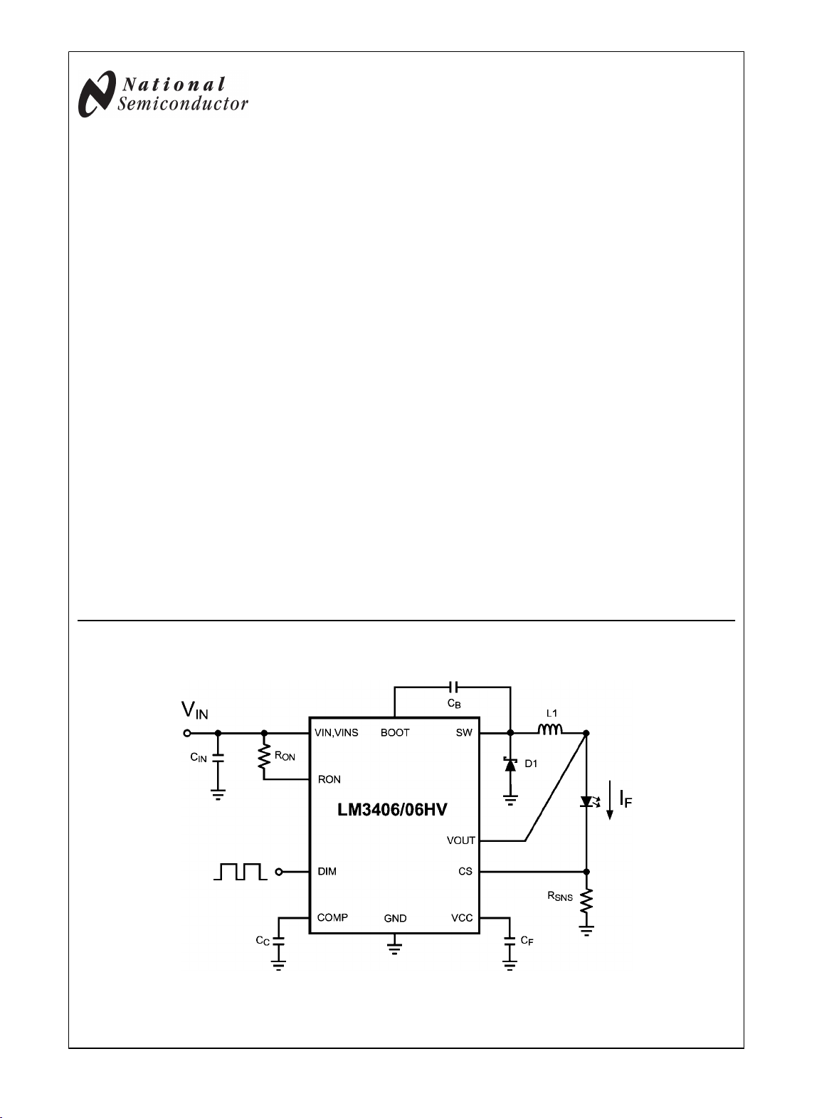
Typical Application
Features
Integrated 2.0A MOSFET
■
VIN Range 6V to 42V (LM3406)
■
VIN Range 6V to 75V (LM3406HV)
■
True average output current control
■
1.7A Minimum Output Current Limit Over Temperature
■
Cycle-by-Cycle Current Limit
■
PWM Dimming with Dedicated Logic Input
■
PWM Dimming with Power Input Voltage
■
Simple Control Loop Compensation
■
Low Power Shutdown
■
Supports All-Ceramic Output Capacitors and Capacitor-
■
less Outputs
Thermal Shutdown Protection
■
eTSSOP-14 Package
■
Applications
LED Driver
■
Constant Current Source
■
Automotive Lighting
■
General Illumination
■
Industrial Lighting
■
30020301
© 2008 National Semiconductor Corporation 300203 www.national.com
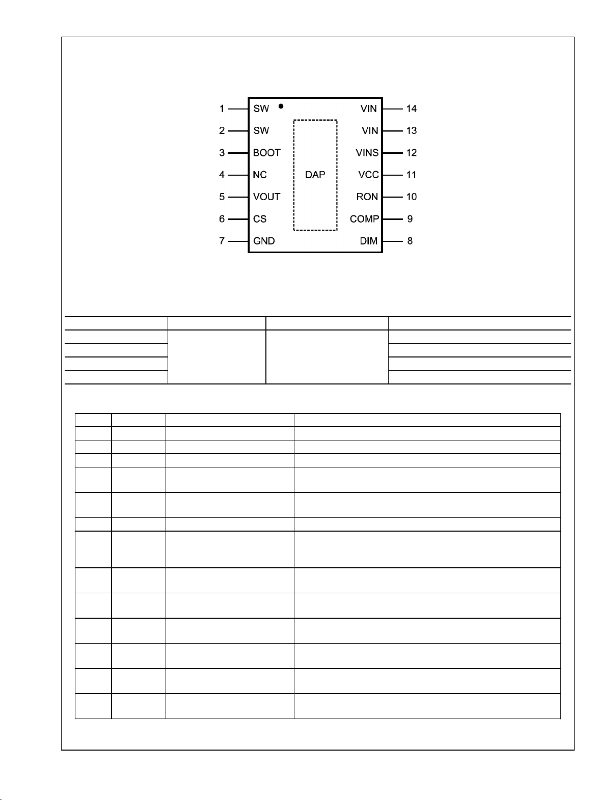
Connection Diagram
LM3406/LM3406HV
LM3406/06HV
14-Lead Exposed Pad Plastic TSSOP Package
NS Package Number MXA14A
30020302
Ordering Information
Order Number Package Type NSC Package Drawing Supplied As
LM3406MH
LM3406MHX 2500 units on tape and reel
LM3406HVMH 95 units in anti-static rails
LM3406HVMHX 2500 units on tape and reel
eTSSOP-14 MXA14A
95 units in anti-static rails
Pin Descriptions
Pin(s) Name Description Application Information
1,2 SW Switch pin Connect these pins to the output inductor and Schottky diode.
3 BOOT MOSFET drive bootstrap pin Connect a 22 nF ceramic capacitor from this pin to the SW pins.
4 NC No Connect No internal connection. Leave this pin unconnected.
5 VOUT Output voltage sense pin Connect this pin to the output node where the inductor and the first
LED's anode connect.
6 CS Current sense feedback pin Set the current through the LED array by connecting a resistor from
this pin to ground.
7 GND Ground pin Connect this pin to system ground.
8 DIM Input for PWM dimming Connect a logic-level PWM signal to this pin to enable/disable the
power MOSFET and reduce the average light output of the LED array.
Logic high = output on, logic low - output off.
9 COMP Error amplifier output Connect a 0.1 µF ceramic capacitor with X5R or X7R dielectric from
this pin to ground.
10 RON On-time control pin A resistor connected from this pin to VIN sets the regulator controlled
on-time.
11 VCC Output of the internal 7V linear
regulator
12 VINS Input voltage PWM dimming
comparator input
13,14 VIN Input voltage pin Nominal operating input range for this pin is 6V to 42V (LM3406) or 6V
DAP DAP Thermal Pad Connect to ground. Place 4-6 vias from DAP to bottom layer ground
Bypass this pin to ground with a minimum 0.1 µF ceramic capacitor
with X5R or X7R dielectric.
Connect this pin to the anode of the input diode to allow dimming by
PWM of the input voltage
to 75V (LM3406HV).
plane.
www.national.com 2
LM3406/LM3406HV
Absolute Maximum Ratings LM3406/LM3406HV (Note 1)
If Military/Aerospace specified devices are required,
please contact the National Semiconductor Sales Office/
Distributors for availability and specifications.
VIN to GND -0.3V to 45V
(76V LM3406HV)
VINS to GND -0.3V to 45V
(76V LM3406HV)
COMP to GND -0.3V to 7V
CS to GND -0.3V to 7V
RON to GND -0.3V to 7V
Junction Temperature 150°C
Storage Temp. Range -65°C to 125°C
ESD Rating (Note 2) 2kV
Soldering Information
Lead Temperature (Soldering,
10sec) 260°C
Infrared/Convection Reflow (15sec) 235°C
VOUT to GND -0.3V to 45V
(76V LM3406HV)
BOOT to GND -0.3V to 59V
(90V LM3406HV)
SW to GND -1.5V to 45V
(76V LM3406HV)
BOOT to VCC -0.3V to 45V
(76V LM3406HV)
BOOT to SW -0.3V to 14V
VCC to GND -0.3V to 14V
Operating Ratings
(Note 1)
V
IN
Junction Temperature Range −40°C to +125°C
Thermal Resistance θ
JA
(eTSSOP-14 Package)
(Note 4) 50°C/W
6V to 42V
(75V LM3406HV)
DIM to GND -0.3V to 7V
Electrical Characteristics V
= 24V unless otherwise indicated. Typicals and limits appearing in plain type apply
IN
for TA = TJ = +25°C (Note 3). Limits appearing in boldface type apply over full Operating Temperature Range. Datasheet min/
max specification limits are guaranteed by design, test, or statistical analysis.
LM3406/LM3406HV
Symbol Parameter Conditions Min Typ Max Units
REGULATION COMPARATOR AND ERROR AMPLIFIER
V
REF
V
0V
I
CS
I
VOUT
I
COMP
G
m-CS
SHUTDOWN
V
SD-TH
V
SD-HYS
ON AND OFF TIMER
t
OFF-MIN
t
ON
t
ON-MIN
VINS COMPARATOR
V
INS-TH
I
IN-2WD
INTERNAL REGULATOR
V
CC-REG
V
IN-DO
V
CC-BP-TH
V
CC-LIM
CS Regulation Threshold CS Decreasing, SW turns on 187.5 200 210 mV
191.0
(Note 5)
210.0
(Note 5)
CS Over-voltage Threshold CS Increasing, SW turns off 300 mV
CS Bias Current CS = 0V 0.9 µA
VOUT Bias Current VOUT = 24V 83 µA
COMP Pin Current CS = 0V 25 µA
Error Amplifier
150 mV < CS < 250 mV 145 µS
Transconductance
Shutdown Threshold RON Increasing 0.3 0.7 1.05 V
Shutdown Hysteresis RON Decreasing 40 mV
Minimum Off-time CS = 0V 230 ns
Programmed On-time
VIN = 24V, VO = 12V, RON = 200 kΩ
800 1300 1800
Minimum On-time 280
VINS Pin Threshold VINS decreasing 70 %VIN
VINS Pin Input Current VINS = 24V * 0.7 25 µA
VCC Regulated Output 0 mA < ICC < 5 mA 6.4 7 7.4 V
VIN - V
CC
ICC = 5 mA, 6.0V < VIN < 8.0V, Non-
300 mV
switching
VCC Bypass Threshold VIN Increasing 8.8 V
VCC Current Limit VIN = 24V, VCC = 0V 4 20 mA
3 www.national.com
Symbol Parameter Conditions Min Typ Max Units
V
CC-UV-TH
VCC Under-voltage Lock-out
VCC Increasing 5.3 V
Threshold
V
CC-UV-HYS
VCC Under-voltage Lock-out
VCC Decreasing 150 mV
Hysteresis
I
IN-OP
LM3406/LM3406HV
I
IN-SD
I
Operating Current Non-switching, CS = 0.5V 1.2 mA
IN
IIN Shutdown Current RON = 0V 240 350 µA
CURRENT LIMIT
I
LIM
Current Limit Threshold 1.7 2.1 2.7 A
DIM COMPARATOR
V
IH
V
IL
I
DIM-PU
Logic High DIM Increasing 2.2 V
Logic Low DIM Decreasing 0.8 V
DIM Pull-up Current DIM = 1.5V 80 µA
MOSFET AND DRIVER
R
DS-ON
V
DR-UVLO
Buck Switch On Resistance ISW = 200 mA, BOOT = 6.3V 0.37 0.75
BOOT Under-voltage Lock-out
BOOT–SW Increasing 1.7 2.9 4.3 V
Threshold
V
DR-HYS
BOOT Under-voltage Lock-out
BOOT–SW Decreasing 370 mV
Hysteresis
THERMAL SHUTDOWN
T
SD
T
SD-HYS
Thermal Shutdown Threshold 165 °C
Thermal Shutdown Hysteresis 25 °C
THERMAL RESISTANCE
θ
JA
Note 1: Absolute Maximum Ratings indicate limits beyond which damage to the device may occur, including inoperability and degradation of device reliability
and/or performance. Functional operation of the device and/or non-degradation at the Absolute Maximum Ratings or other conditions beyond those indicated in
the Operating Ratings is not implied. The recommended Operating Ratings indicate conditions at which the device is functional and the device should not be
operated beyond such conditions.
Note 2: The human body model is a 100 pF capacitor discharged through a 1.5 kΩ resistor into each pin.
Note 3: Typical values represent most likely parametric norms at the conditions specified and are not guaranteed.
Note 4: θJA of 50°C/W with DAP soldered to a minimum of 2 square inches of 1oz. copper on the top or bottom PCB layer.
Note 5: Specified with junction temperature from 0°C - 125°C.
Note 6: VIN = 24V, IF = 1A, TA = 25°C, and the load consists of three InGaN LEDs in series unless otherwise noted. See the Bill of Materials table at the end of
the datasheet.
Junction to Ambient eTSSOP-14 Package (Note 4) 50 °C/W
Ω
www.national.com 4
Typical Performance Characteristics
LM3406/LM3406HV
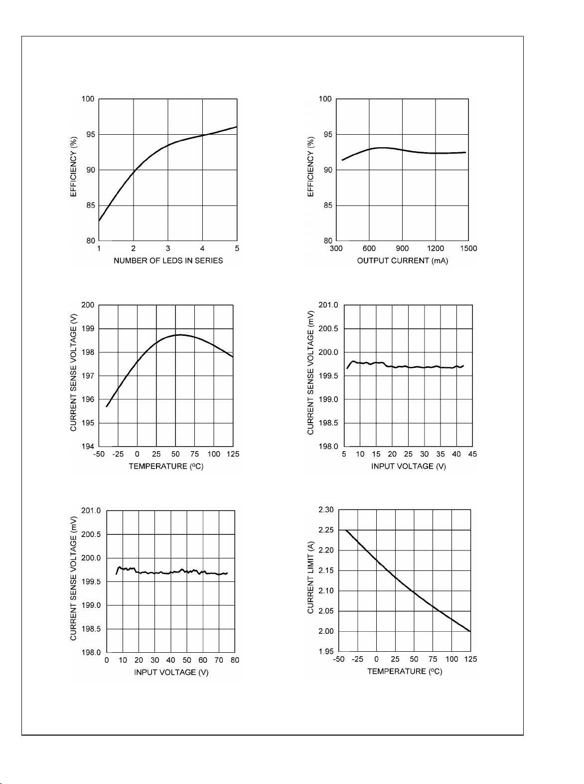
Efficiency Vs. Number of InGaN LEDs in Series
(Note 6)
30020363
V
vs Temperature
REF
Efficiency Vs. Output Current
(Note 6)
V
vs VIN, LM3406
REF
30020364
V
vs VIN, LM3406HV
REF
30020335
30020337
30020336
Current Limit vs Temperature
30020338
5 www.national.com
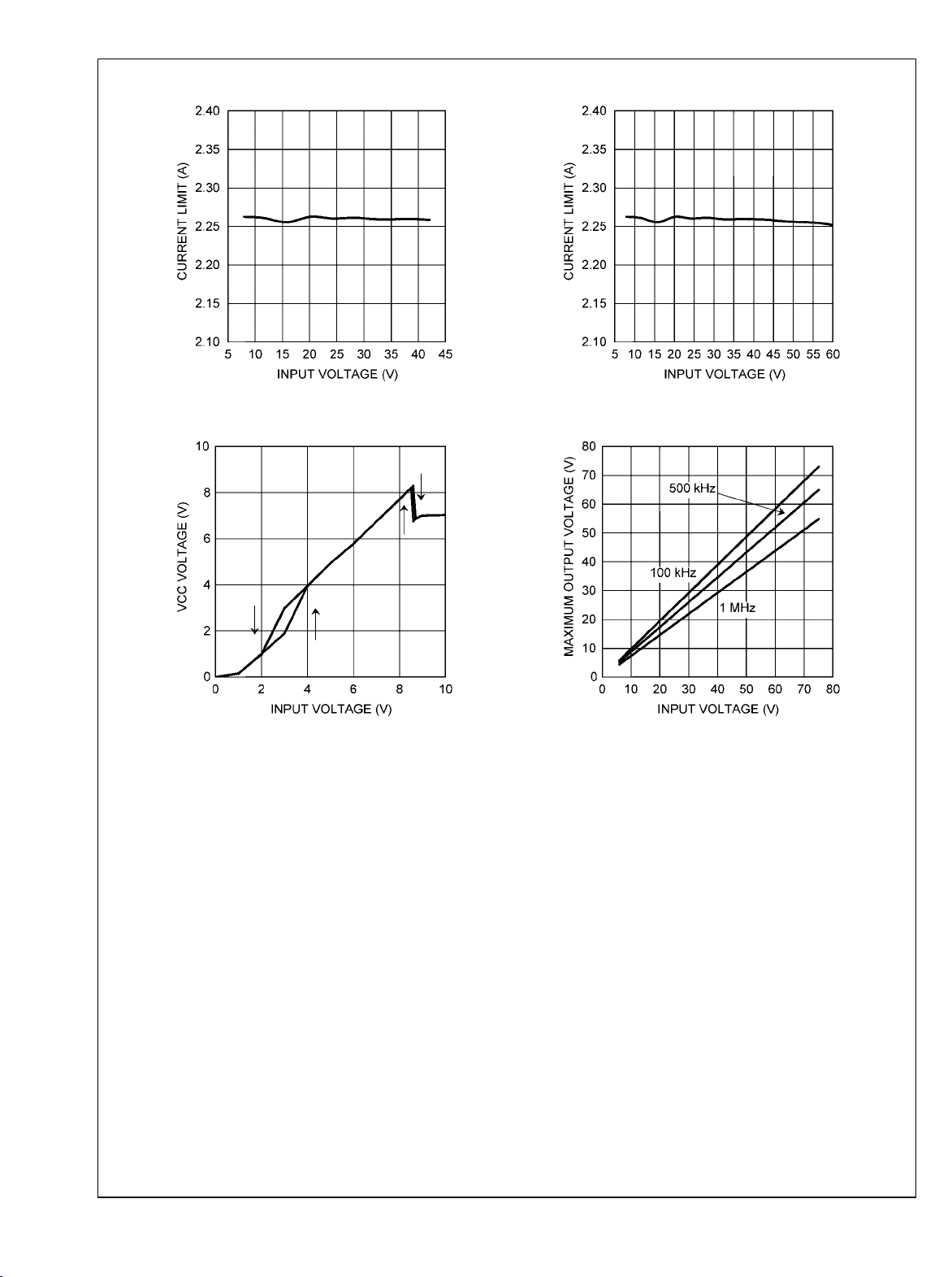
Current Limit vs VIN, LM3406
LM3406/LM3406HV
Current Limit vs VIN, LM3406HV
VCC vs V
30020339
V
IN
30020341
vs VIN, LM3406
O-MAX
30020340
30020342
www.national.com 6
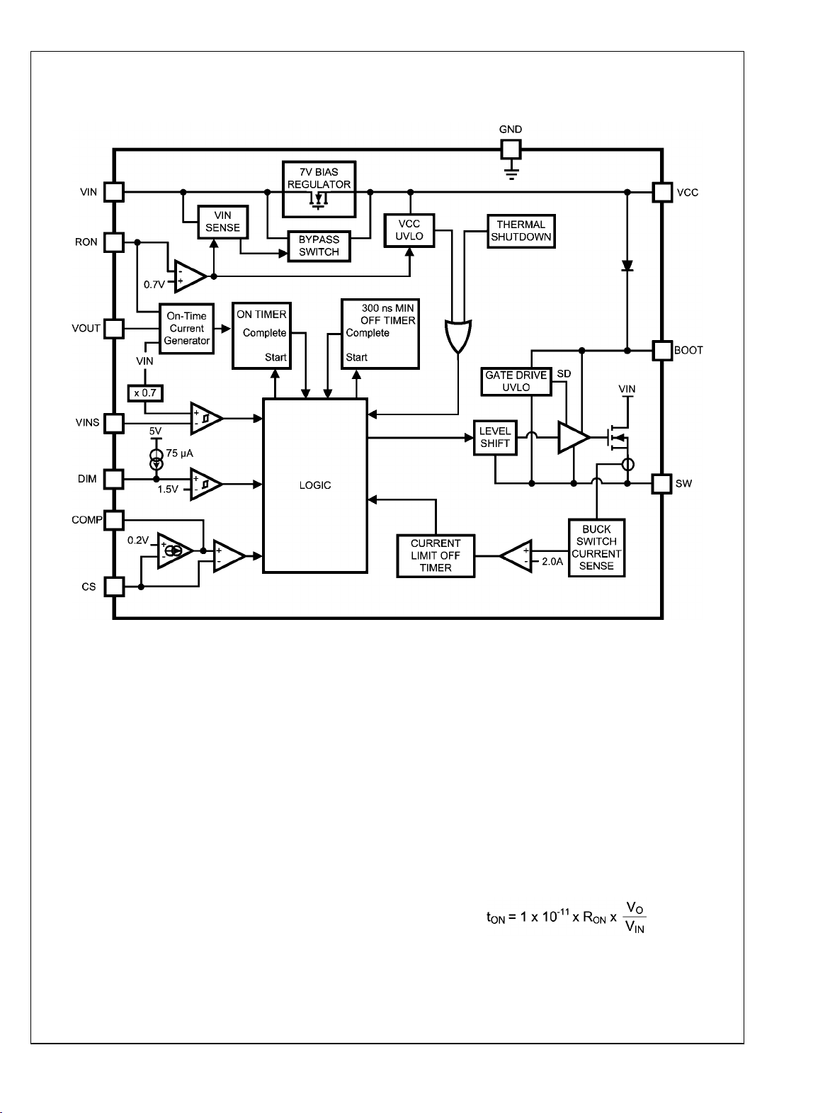
Block Diagram
LM3406/LM3406HV
Application Information
THEORY OF OPERATION
The LM3406 and LM3406HV are buck regulators with a wide
input voltage range, low voltage reference, and a fast output
enable/disable function. These features combine to make
them ideal for use as a constant current source for LEDs with
forward currents as high as 1.5A. The controlled on-time
(COT) architecture uses a comparator and a one-shot ontimer that varies inversely with input and output voltage instead of a fixed clock. The LM3406/06HV also employs an
integrator circuit that averages the output current. When the
converter runs in continuous conduction mode (CCM) the
controlled on-time maintains a constant switching frequency
over changes in both input and output voltage. These features
combine to give the LM3406/06HV an accurate output current, fast transient response, and constant switching frequency over a wide range of conditions.
30020303
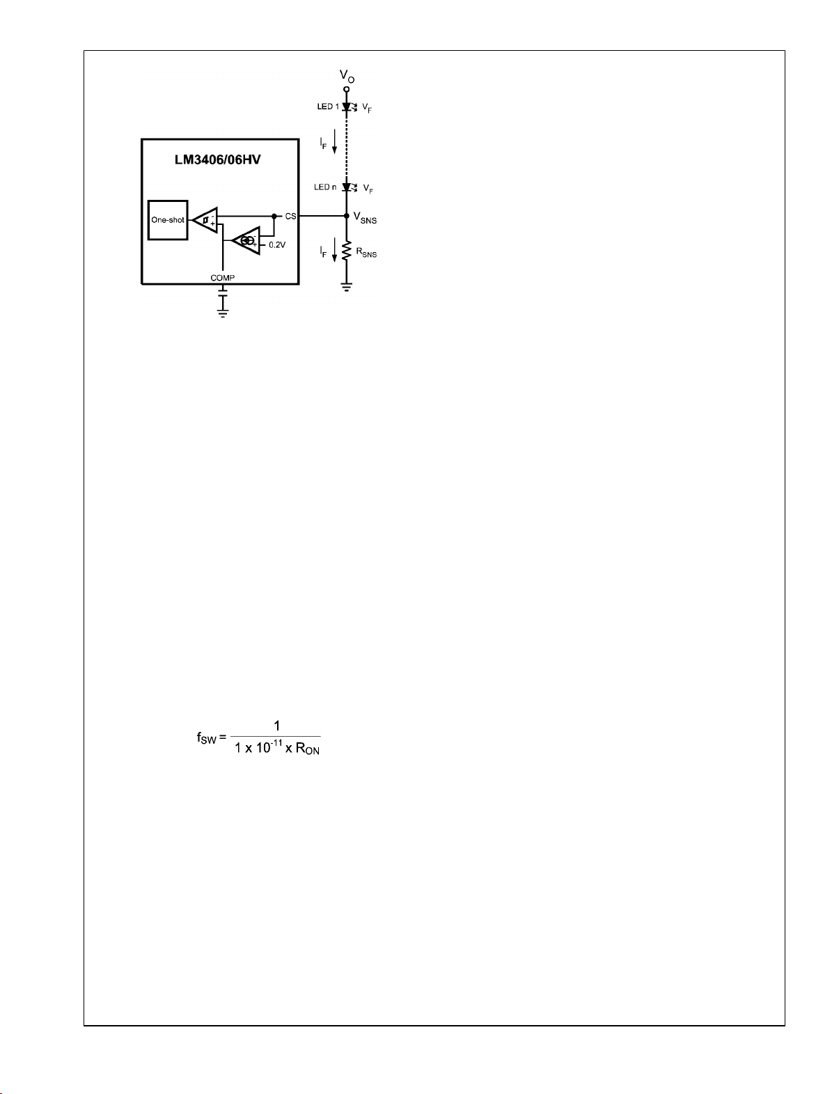
CONTROLLED ON-TIME OVERVIEW
Figure 1 shows a simplified version of the feedback system
used to control the current through an array of LEDs. A differential voltage signal, V
flows through the current setting resistor, R
back by the CS pin, where it is integrated and compared
, is created as the LED current
SNS
SNS
. V
SNS
is fed
against an error amplifier-generated reference. The error amplifier is a transconductance (Gm) amplifier which adjusts the
voltage on COMP to maintain a 200 mV average at the CS
pin. The on-comparator turns on the power MOSFET when
V
falls below the reference created by the Gm amp. The
SNS
power MOSFET conducts for a controlled on-time, tON, set by
an external resistor, RON, the input voltage, VIN and the output
voltage, VO. On-time can be estimated by the following simplified equation (for the most accurate version of this expression see the Appendix):
At the conclusion of tON the power MOSFET turns off and
must remain off for a minimum of 230 ns. Once this t
is complete the CS comparator compares the integrated
V
and reference again, waiting to begin the next cycle.
SNS
OFF-MIN
7 www.national.com
LM3406/LM3406HV
FIGURE 1. Comparator and One-Shot
SWITCHING FREQUENCY
The LM3406/06HV does not contain a clock, however the ontime is modulated in proportion to both input voltage and
output voltage in order to maintain a relatively constant frequency. On-time tON, duty cycle D and switching frequency
fSW are related by the following expression:
fSW = D / t
D = (VO + VD) / (VIN - VSW + VD)
VD = Schottky diode (typically 0.5V)
VSW = IF x R
The LM3406/06HV regulators should be operated in continuous conduction mode (CCM), where inductor current stays
positive throughout the switching cycle. During steady-state
CCM operation, the converter maintains a constant switching
frequency that can be estimated using the following equation
(for the most accurate version see the Appendix):
ON
DSON
30020306
output voltage of the LM3406/06HV is limited by the minimum
off-time as well. V
driven in series. Referring to the illustration in Figure 1, output
determines how many LEDs can be
O-MAX
voltage is calculated as:
V
t
OFF-MIN
O-MAX
= 230 ns
= V
x (1 - fSW x t
IN-MIN
OFF-MIN
)
Once V
series LEDs, n
sion and rounding down:
has been calculated, the maximum number of
O-MAX
, can be calculated by the following espres-
MAX
n
MAX
= V
O-MAX
/ V
F
VF = forward voltage of each LED
At low switching frequency V
LM3406/06HV to regulate output voltages that are nearly
is higher, allowing the
O-MAX
equal to input voltage, and this can allow the system to drive
more LEDs in series. Low switching frequencies are not always desireable, however, because they require larger, more
expensive components.
CALCULATING OUTPUT VOLTAGE
Even though output current is the controlled parameter in LED
drivers, output voltage must still be calculated in order to design the complete circuit. Referring to the illustration in Figure
1, output voltage is calculated as:
VO = n x VF + V
V
= sense voltage of 200 mV, n = number of LEDs in series
SNS
SNS
MINIMUM ON-TIME
The minimum on-time for the LM3406/06HV is 280 ns (typical). One practical example of reaching the minimum on-time
is when dimming the LED light output with a power FET
placed in parallel to the LEDs. When the FET is on, the output
voltage drops to 200 mV. This results in a small duty cycle
and in most circuits requires an on-time that would be less
than 280 ns. In such a case the LM3406/06HV keeps the ontime at 280 ns and increases the off-time as much as needed,
which effectively reduces the switching frequency.
SETTING LED CURRENT
LED current is set by the resistor R
mined using the following simple expression due to the output
, which can be deter-
SNS
averaging:
R
= 0.2 / I
SNS
F
MAXIMUM NUMBER OF SERIES LEDS
LED driver designers often want to determine the highest
number of LEDs that can be driven by their circuits. The limit
on the maximum number of series LEDs is set by the highest
output voltage, V
buck regulator cannot provide an output voltage that is higher
, that the LED driver can provide. A
O-MAX
than the minimum input voltage, and in pratice the maximum
www.national.com 8
HIGH VOLTAGE BIAS REGULATOR
The LM3406/06HV contains an internal linear regulator with
a 7V output, connected between the VIN and the VCC pins.
The VCC pin should be bypassed to the GND pin with a 0.1
µF ceramic capacitor connected as close as possible to the
pins of the IC. VCC tracks VIN until VIN reaches 8.8V (typical)
and then regulates at 7V as VIN increases. The
LM3406/06HV comes out of UVLO and begins operating
when VCC crosses 5.3V. This is shown graphically in the
Typical Performance curves.
INTERNAL MOSFET AND DRIVER
The LM3406/06HV features an internal power MOSFET as
well as a floating driver connected from the SW pin to the
BOOT pin. Both rise time and fall time are 20 ns each (typical)
and the approximate gate charge is 9 nC. The high-side rail
for the driver circuitry uses a bootstrap circuit consisting of an
internal high-voltage diode and an external 22 nF capacitor,
CB. VCC charges CB through the internal diode while the power
MOSFET is off. When the MOSFET turns on, the internal
diode reverse biases. This creates a floating supply equal to
 Loading...