

National Semiconductor LM3352 Technical data
September 1999
LM3352
Regulated 200 mA Buck-Boost Switched Capacitor
DC/DC Converter
LM3352 Regulated 200 mA Buck-Boost Switched Capacitor DC/DC Converter
General Description
The LM3352 is a CMOS switched capacitor DC/DC converter that produces a regulated output voltage by automatically stepping up (boost) or stepping down (buck) the input
voltage. It accepts an input voltage between 2.5V and 5.5V.
The LM3352 is available in three standard output voltage
versions: 2.5V, 3.0V and 3.3V. If other output voltage options
between 1.8V and 4.0V are desired, please contact your
National Semiconductor representative.
The LM3352’s proprietary buck-boost architecture enables
up to 200 mA of load current at an average efficiency greater
than 80%. Typical operating current is only 400 µA and the
typical shutdown current is only 2.5 µA.
The LM3352 is available in a 16-pin TSSOP package. This
package has a maximum height of only 1.1 mm.
The high efficiency of the LM3352, low operating and shutdown currents, small package size, and the small size of the
overall solution make this device ideal for battery powered,
portable, and hand-held applications.
Features
n Regulated V
n Standard output voltage options: 2.5V, 3.0V and 3.3V
n Custom output voltages available from 1.8V to 4.0V in
100 mV increments
n 2.5V to 5.5V input voltage
n Up to 200 mA output current
>
n
80% average efficiency
n Uses few, low-cost external components
n Very small solution size
n 400 µA typical operating current
n 2.5 µA typical shutdown current
n 1 MHz switching frequency (typical)
n Architecture and control methods provide high load
current and good efficiency
n TSSOP-16 package
n Over-temperature protection
with±3% accuracy
OUT
Applications
n 1-cell Lilon battery-operated equipment including PDAs,
hand-held PCs, cellular phones
n Flat panel displays
n Hand-held instruments
n NiCd, NiMH, or alkaline battery powered systems
n 3.3V to 2.5V and 5.0V to 3.3V conversion
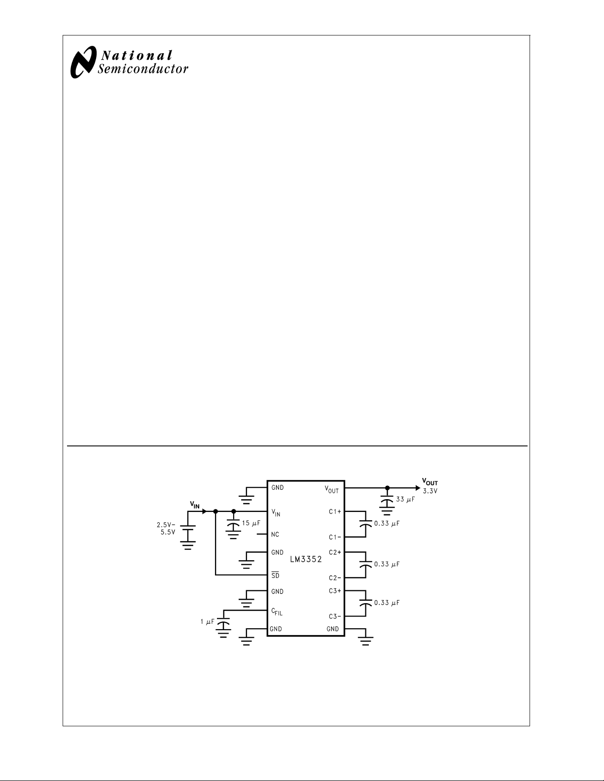
Typical Operating Circuit
10103701
© 2004 National Semiconductor Corporation DS101037 www.national.com
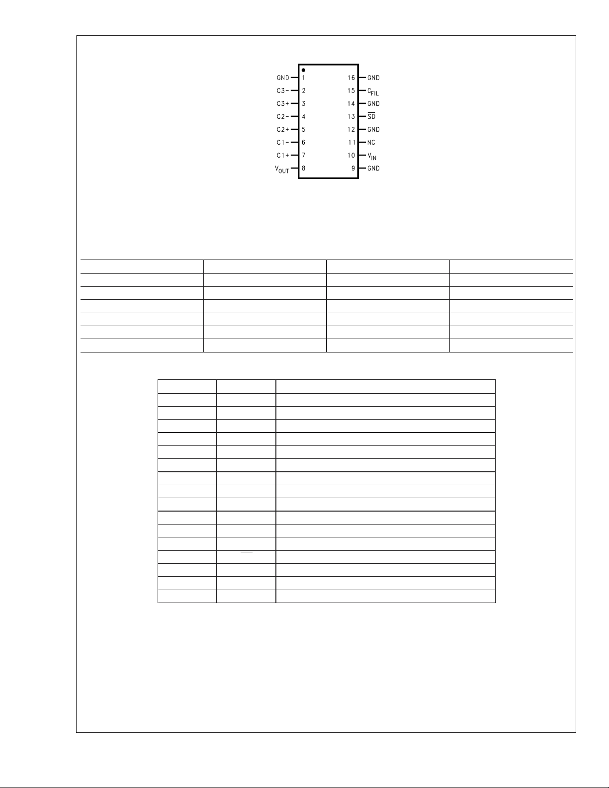
Connection Diagram
LM3352
Top View
TSSOP-16 Pin Package
See NS Package Number MTC16
10103702
Ordering Information
Order Number Package Type NSC Package Drawing Supplied As
LM3352MTCX-2.5 TSSOP-16 MTC16 2.5k Units, Tape and Reel
LM3352MTC-2.5 TSSOP-16 MTC16 94 Units, Rail
LM3352MTCX-3.0 TSSOP-16 MTC16 2.5k Units, Tape and Reel
LM3352MTC-3.0 TSSOP-16 MTC16 94 Units, Rail
LM3352MTCX-3.3 TSSOP-16 MTC16 2.5k Units, Tape and Reel
LM3352MTC-3.3 TSSOP-16 MTC16 94 Units, Rail
Pin Description
Pin Number Name Function
1 GND Ground*
2 C3− Negative Terminal for C3
3 C3+ Positive Terminal for C3
4 C2− Negative Terminal for C2
5 C2+ Positive Terminal for C2
6 C1− Negative Terminal for C1
7 C1+ Positive Terminal for C1
8V
9 GND Ground*
10 V
11 NC This pin must be left unconnected.
12 GND Ground*
13 SD
14 GND Ground*
15 C
16 GND Ground*
OUT
IN
FIL
Regulated Output Voltage
Input Supply Voltage
Active Low CMOS Logic-Level Shutdown Input
Filter Capacitor;A1µFceramic capacitor is suggested.
*All GND pins of the LM3352 must be connected to the same ground.
www.national.com 2
LM3352
Absolute Maximum Ratings (Note 1)
If Military/Aerospace specified devices are required,
please contact the National Semiconductor Sales Office/
Distributors for availability and specifications.
Pin −0.5V to 4.5V
V
OUT
All Other Pins −0.5V to 5.6V
Power Dissipation (T
= 25˚C)
A
Operating Ratings
Input Voltage (VIN) 2.5V to 5.5V
Output Voltage (V
Ambient Temperature (T
Junction Temperature (T
) 1.8V to 4.0V
OUT
) (Note 2) −40˚C to +85˚C
A
) (Note 2) −40˚C to +125˚C
J
(Note 2) 700 mW
(Note 2) 150˚C
T
JMAX
θ
(Note 2) 150˚C/W
JA
Storage Temperature −65˚C to +150˚C
Lead Temperature (Soldering, 5
sec.) 260˚C
ESD Rating (Note 3)
human body model
machine model
2kV
100V
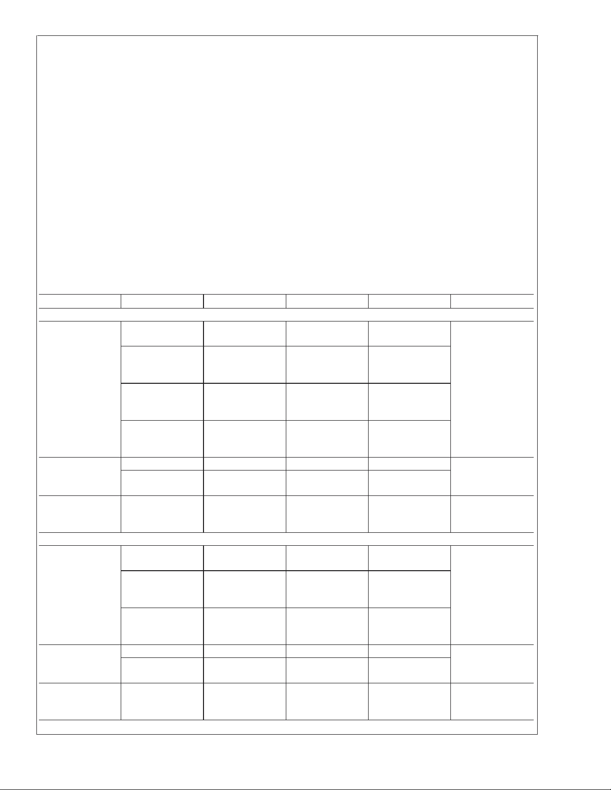
Electrical Characteristics
Limits in standard typeface are for TJ= 25˚C, and limits in boldface type apply over the full operating temperature range. Unless otherwise specified: C
1=C2=C3
= 0.33 µF; CIN= 15 µF; C
Parameter Conditions Min Typ Max Units
LM3352-2.5
Output Voltage (V
OUT
)
V
= 3.5V; I
IN
100 mA
<
2.8V
1mA
=
LOAD
<
V
5.5V;
IN
<
I
LOAD
<
2.463 2.5 2.537
2.425/2.400 2.5 2.575/2.600
100 mA
<
3.6V
1mA
<
V
4.9V;
IN
<
I
LOAD
<
2.425/2.400 2.5 2.575/2.600
200 mA
<
4.9V
1mA
<
V
5.5V;
IN
<
I
LOAD
<
2.425/2.400 2.5 2.575/2.600
175 mA
Efficiency I
=15mA 85
LOAD
I
= 150 mA, V
LOAD
IN
= 4.0V
Output Voltage
Ripple
(Peak-to-Peak)
=50mA
I
LOAD
C
OUT
tantalum
=33µF
LM3352-3.0
Output Voltage (V
OUT
)
V
= 3.5V; I
IN
100 mA
<
2.5V
1mA
=
LOAD
<
V
5.5V;
IN
<
I
LOAD
<
2.955 3.0 3.045
2.910/2.880 3.0 3.090/3.120
100 mA
<
3.8V
1mA
<
V
5.5V;
IN
<
I
LOAD
<
2.910/2.880 3.0 3.090/3.120
200 mA
Efficiency I
=15mA 80
LOAD
I
= 150 mA, V
LOAD
IN
= 4.0V
Output Voltage
Ripple
(Peak-to-Peak)
=50mA
I
LOAD
C
OUT
tantalum
=33µF
= 33 µF; VIN= 3.5V.
OUT
75
75 mV
75
75 mV
V
%
P-P
V
%
P-P
www.national.com3
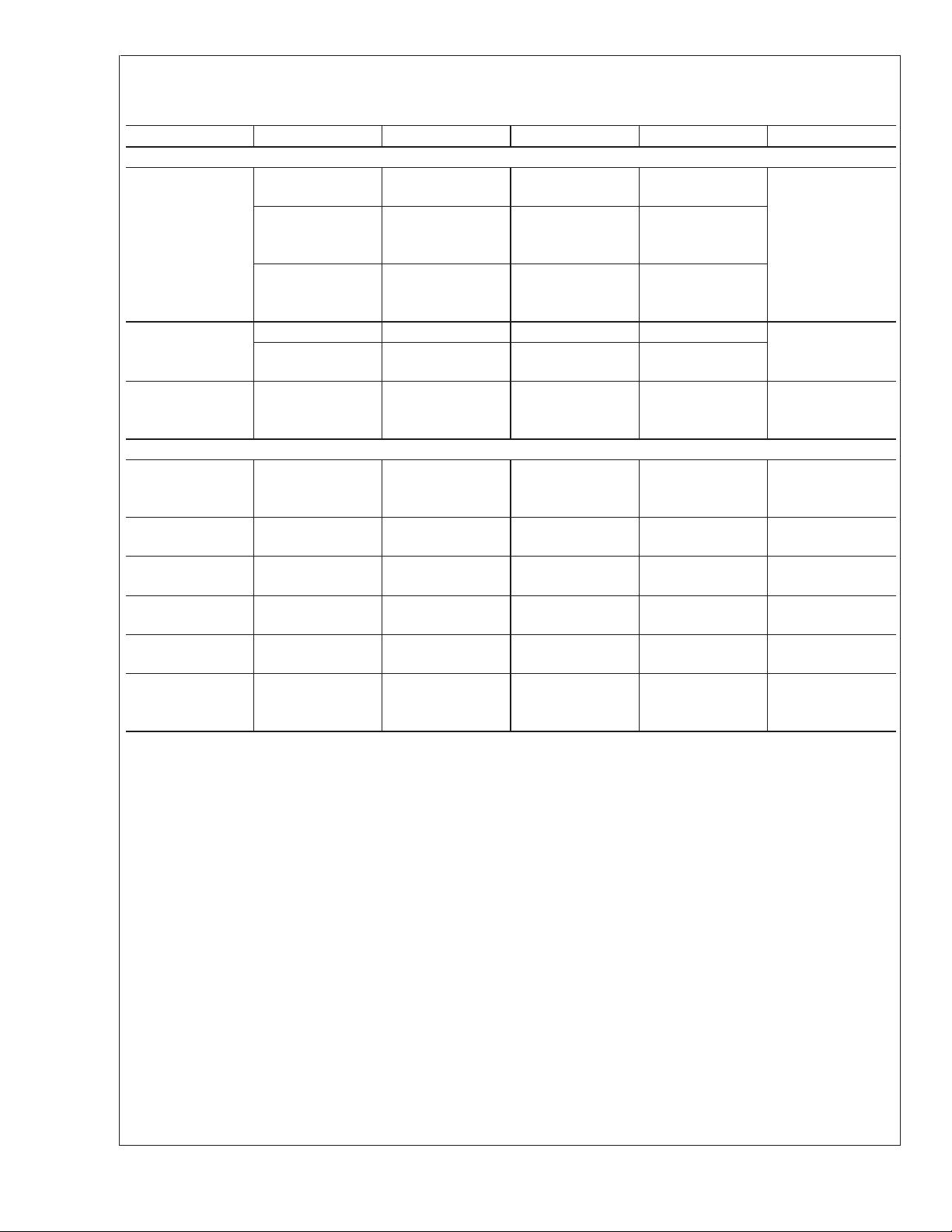
Electrical Characteristics (Continued)
Limits in standard typeface are for TJ= 25˚C, and limits in boldface type apply over the full operating temperature range. Un-
LM3352
less otherwise specified: C
1=C2=C3
Parameter Conditions Min Typ Max Units
LM3352-3.3
Output Voltage (V
OUT
)
V
= 3.5V; I
IN
100 mA
<
2.5V
1mA
V
IN
<
I
LOAD
100 mA
<
4.0V
V
IN
<
1mA
I
LOAD
200 mA
Efficiency I
=15mA 90
LOAD
I
= 150 mA, V
LOAD
= 4.0V
Output Voltage
Ripple
(Peak-to-Peak)
=50mA
I
LOAD
C
OUT
tantalum
=33µF
LM3352-ALL OUTPUT VOLTAGE VERSIONS
Operating Quiescent
Current
Shutdown Quiescent
Current
Measured at Pin
VIN;
= 0A (Note 4)
I
LOAD
SD Pin at 0V (Note
5)
Switching
Frequency
SD Input Threshold
2.5V
<
V
IN
Low
SD Input Threshold
2.5V<V
IN
High
SD Input Current Measured at SD
Pin;
SD Pin = V
Note 1: “Absolute Maximum Ratings” indicate limits beyond which damage to the device may occur. Electrical specifications do not apply when operating the device
beyond its rated operating conditions.
Note 2: As long as T
≤ 5V. For V
at higher ambient temperatures to make sure T
Note 3: The human body model is a 100 pF capacitor discharged through a 1.5 kΩ resistor into each pin. The machine model is a 200 pF capacitor discharged
directly into each pin.
Note 4: The V
Note 5: The output capacitor C
IN
≤ +85˚C, all electrical characteristics hold true for the 3.0V and 3.3V options at all current loads and the 2.5V option at all loads when V
A
>
5V with the 2.5V option, the junction temperature rise above ambient is: ∆T = 540IL−23 where ILis in amps. The output current must be derated
pin is forced to 200 mV above the typical V
OUT
IN
is fully discharged before measurement.
OUT
= 0.33 µF; CIN= 15 µF; C
=
LOAD
<
5.5V;
<
<
5.5V;
<
3.201/3.168 3.3 3.399/3.432
3.201/3.168 3.3 3.399/3.432
IN
3.251 3.3 3.349
= 33 µF; VIN= 3.5V.
OUT
80
75 mV
400 500 µA
2.5 5 µA
0.65 1 1.35 MHz
<
5.5V 0.2 V
<
5.5V 0.8 V
IN
0.1 1.0 µA
= 5.5V
does not exceed 150˚C when operating the 2.5V option at V
J
. This is to insure that the internal switches are off.
OUT
>
5V.
IN
IN
V
%
P-P
V
V
IN
www.national.com 4
 Loading...