

November 2004
LM3200
Miniature, Adjustable, Step-Down DC-DC Converter with
Bypass Mode for RF Power Amplifiers
LM3200 Miniature, Adjustable, Step-Down DC-DC Converter with Bypass Mode for RF Power
Amplifiers
General Description
The LM3200 is a DC-DC converter optimized for powering
RF power amplifiers (PAs) from a single Lithium-Ion cell. It
steps down an input voltage of 2.7V to 5.5V to a variable
output voltage of 0.8V to 3.6V. The output voltage is set
using an analog input ( V
RF PA at various power levels.
The LM3200 offers superior features and performance for
mobile phones and similar RF PA applications. Fixedfrequency PWM mode minimizes RF interference. Bypass
mode turns on an internal bypass switch to power the PA
directly from the battery. LM3200 has both forced and automatic bypass modes. Shutdown mode turns the device off
and reduces battery consumption to 0.1 µA (typ.). The
LM3200 is available in a 10-pin lead free micro SMD package. A high switching frequency (2 MHz) allows use of tiny
surface-mount components. Only three small external
surface-mount components, an inductor and two ceramic
capacitors are required.
) for optimizing efficiency of the
CON
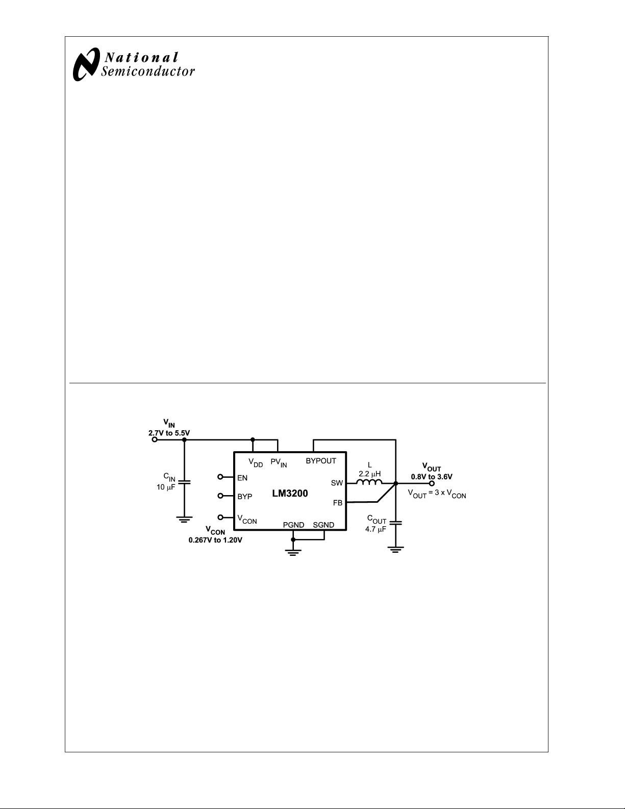
Typical Application
Features
n 2 MHz (typ.) PWM Switching Frequency
n Operates from a single Li-Ion cell (2.7V to 5.5V)
n Variable Output Voltage (0.8V to 3.6V)
n 300 mA Maximum load capability (PWM mode)
n 500 mA Maximum load capability (Bypass mode)
n PWM, Forced and Automatic Bypass Mode
n High Efficiency (96% Typ at 3.6V
from internal synchronous rectification
n 10-pin micro SMD Package
n Current Overload Protection
n Thermal Overload Protection
, 3.2V
IN
at 120 mA)
OUT
Applications
n Cellular Phones
n Hand-Held Radios
n RF PC Cards
n Battery Powered RF Devices
20126101
© 2004 National Semiconductor Corporation DS201261 www.national.com
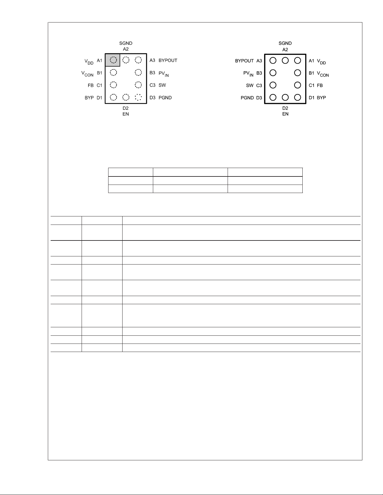
Connection Diagrams
LM3200
Top View
20126102
Bottom View
20126103
10–Bump Thin Micro SMD Package, Large Bump
See NS Package Number TLP10NHA
Order Information
Order Number Package Marking (Note) Supplied As
LM3200TL XYTT SCUB 250 Units, Tape and Reel
LM3200TLX XYTT SCUB 3000 Units, Tape and Reel
Note: The package marking “XY” designates the date code. “TT” is a NSC internal code for die traceability.
Pin Description
Pin # Name Description
A1 V
B1 V
DD
CON
C1 FB Feedback Analog Input. Connect to the output at the output filter capacitor. (Figure 1)
D1 BYP Bypass. Use this digital input to command operation in Bypass mode. Set BYP low for normal
D2 EN Enable Input. Set this digital input high after Vin
D3 PGND Power Ground
C3 SW Switching Node connection to the internal PFET switch and NFET synchronous rectifier.
B3 PV
IN
A3 BYPOUT Bypass FET Drain. Connect to the output capacitor. (Figure 1) Do not leave floating.
A2 SGND Analog and Control Ground
Analog Supply Input. A 0.1 µF ceramic capacitor is recommended to be placed as close to this
pin as possible. (Figure 1)
Voltage Control Analog input. V
CON
controls V
in PWM mode. Set: V
OUT
OUT
=3xV
CON.
leave floating.
operation.
>
2.7V for normal operation. For shutdown, set
low.
Connect to an inductor with a saturation current rating that exceeds the maximum Switch Peak
Current Limit specification of the LM3200.
Power Supply Voltage Input to the internal PFET switch and Bypass FET. (Figure 1)
Do not
www.national.com 2
LM3200
Absolute Maximum Ratings (Notes 1, 2)
If Military/Aerospace specified devices are required,
please contact the National Semiconductor Sales Office/
Distributors for availability and specifications.
,PVINto SGND −0.2V to +6.0V
V
DD
PGND to SGND −0.2V to +0.2V
EN, FB, BYP, V
CON
SW, BYPOUT (PGND −0.2V)
PVINto V
DD
Continuous Power Dissipation
(SGND −0.2V)
+0.2V)
to (V
DD
w/6.0V max
IN
+0.2V)
to (PV
w/6.0V max
−0.2V to +0.2V
ESD Rating (Note 4)
Human Body Model: All other pins
Human Body Model: PV
Machine Model: All pins
Operating Ratings (Notes 1, 2)
Input Voltage Range 2.7V to 5.5V
Recommended Load Current
PWM Mode 0 mA to 300 mA
Bypass Mode 0 mA to 500 mA
Junction Temperature (T
Ambient Temperature (T
(Note 5)
(Note 3) Internally Limited
Junction Temperature (T
J-MAX)
+150˚C
Storage Temperature Range −65˚C to +150˚C
Maximum Lead Temperature
(Soldering, 10 sec) +260˚C
Thermal Properties
Junction-to-Ambient Thermal 100˚C/W
Resistance (θ
), TLP10 Package (Note 6)
JA
Electrical Characteristics (Notes 2, 7) Limits in standard typeface are for T
face type apply over the full operating ambient temperature range (−25˚C ≤ T
fications apply to the LM3200 with: PV
IN=VDD
= EN = 3.6V, BYP = 0V.
≤ +85˚C). Unless otherwise noted, speci-
A=TJ
2.0 kV
pin
IN
1.0 kV
200V
) Range −25˚C to +125˚C
J
) Range
A
A=TJ
= 25˚C. Limits in bold-
−25˚C to +85˚C
Symbol Parameter Conditions Min Typ Max Units
V
IN
V
FB, MIN
V
FB, MAX
OVP Over-Voltage
V
BYPASS−
V
BYPASS+
I
SHDN
I
Q_PWM
I
Q_BYP
R
DSON (P)
R
DSON (N)
R
DSON
(BYP)
I
LIM-PFET
I
LIM-BYP
F
OSC
V
IH
Input Voltage Range
(Note 8)
Feedback Voltage at
Minimum Setting
Feedback Voltage at
Maximum Setting
Protection Threshold
Auto Bypass Detection
Negative Threshold
Auto Bypass Detection
Positive Threshold
Shutdown Supply
Current (Note 11)
DC Bias Current into
V
DD
Pin-Pin Resistance for
PFET
Pin-Pin Resistance for
N-FET
Pin-Pin Resistance for
Bypass FET
PVIN=VDD=V
V
= 0.267V, VIN= 3.6V
CON
V
= 1.20V, VIN= 4.2V
CON
(Note 9)
(Note 10)
(Note 10)
EN = SW = BYPOUT = V
V
= 0.267V, FB = 2V, No-Load 720 850 µA
CON
BYP = 3.6V, V
ISW= 500mA
ISW= - 200mA
I
BYPOUT
CON
= 500mA
IN
2.7 5.5 V
0.75 0.800 0.85 V
3.528 3.600 3.672 V
330 400 mV
160 250 320 mV
350 450 540 mV
=FB=0V
CON
0.1 3 µA
= 0V, No-Load 720 850 µA
320 450 mΩ
310 450 mΩ
85 120 mΩ
Switch Current Limit (Note 12) 700 820 940 mA
Bypass FET Current
Limit
Internal Oscillator
Frequency
Logic High Input
Threshold for EN, BYP
(Note 13)
800 1000 1200 mA
1.7 2 2.2 MHz
1.20 V
www.national.com3
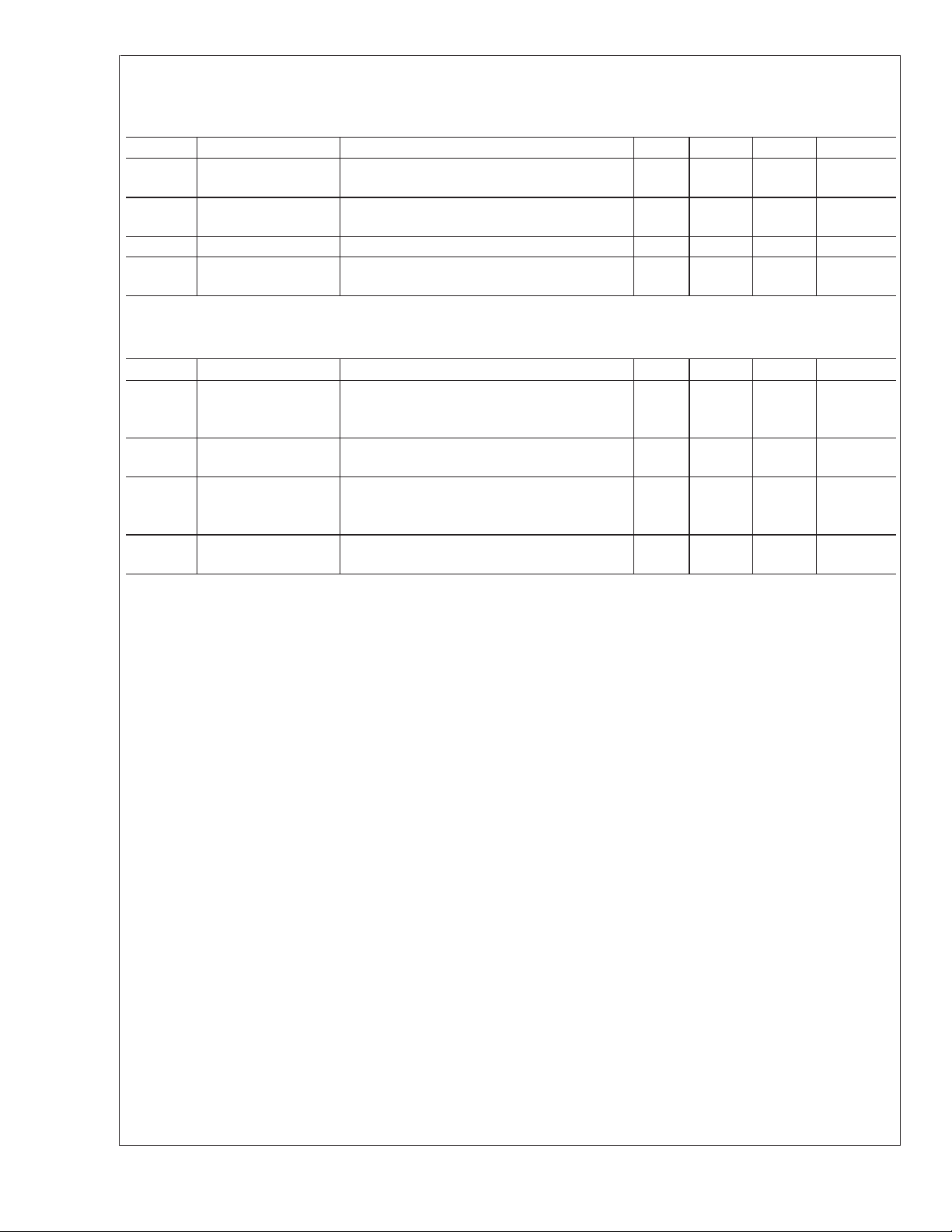
Electrical Characteristics (Notes 2, 7) Limits in standard typeface are for T
type apply over the full operating ambient temperature range (−25˚C ≤ T
LM3200
specifications apply to the LM3200 with: PV
IN=VDD
= EN = 3.6V, BYP = 0V. (Continued)
A=TJ
≤ +85˚C). Unless otherwise noted,
= 25˚C. Limits in boldface
A=TJ
Symbol Parameter Conditions Min Typ Max Units
V
IL
I
PIN
Gain V
I
CON
Logic Low Input
Threshold for EN, BYP
Pin Pull Down Current
for EN, BYP
CON
V
CON
to V
Input Leakage
Gain 3 V/V
OUT
Current
EN, BYP = 3.6V
V
= 1.2V
CON
0.4 V
5 10 µA
10 nA
System Characteristics The following spec table entries are guaranteed by design if the component values
in the typical application circuit are used. These parameters are not guaranteed by production testing.
Symbol Parameter Conditions Min Typ Max Units
T
RESPONSE
C
CON
T
ON_BYP
T
BYP
Time for V
OUT
to Rise
from 0.8V to 3.4V in
PWM Mode
V
Input
CON
Capacitance
Bypass FET Turn On
Time In Bypass Mode
Auto Bypass Detect
Delay Time
V
R
IN
LOAD
= 4.2V, C
=15Ω
OUT
= 4.7 µF,
L = 2.2 uH
V
= 1V,
CON
Test frequency = 100 kHz
VIN= 3.6V, V
= 4.7 µF, R
C
OUT
CON
= 0.267V,
=15Ω
LOAD
BYP = Low to High
(Note 10)
25 µs
15 pF
30 µs
10 15 20 µs
Note 1: Absolute Maximum Ratings indicate limits beyond which damage to the component may occur. Operating Ratings are conditions under which operation of
the device is guaranteed. Operating Ratings do not imply guaranteed performance limits. For guaranteed performance limits and associated test conditions, see the
Electrical Characteristics tables.
Note 2: All voltages are with respect to the potential at the GND pins.
Note 3: Internal thermal shutdown circuitry protects the device from permanent damage. Thermal shutdown engages at T
130˚C (typ.).
Note 4: The Human body model is a 100 pF capacitor discharged through a 1.5 kΩ resistor into each pin. (MIL-STD-883 3015.7) The machine model is a 200 pF
capacitor discharged directly into each pin.
Note 5: In applications where high power dissipation and/or poor package thermal resistance is present, the maximum ambient temperature may have to be
de-rated. Maximum ambient temperature (T
dissipation of the device in the application (P
following equation: T
Note 6: Junction-to-ambient thermal resistance (θ
standard JESD51-7. A 1" x 1", 4 layer, 1.5 oz. Cu board was used for the measurements.
Note 7: Min and Max limits are guaranteed by design, test, or statistical analysis. Typical numbers are not guaranteed, but do represent the most likely norm.
Note 8: The LM3200 is designed for mobile phone applications where turn-on after power-up is controlled by the system controller and where requirements for a
small package size overrule increased die size for internal Under Voltage Lock-Out (UVLO) circuitry. Thus, it should be kept in shutdown by holding the EN pin low
until the input voltage exceeds 2.7V.
Note 9: Over-Voltage protection (OVP) threshold is the voltage above the nominal VOUT where the OVP comparator turns off the PFET switch while in PWM mode.
Note 10: V
switching FETs turn off. This is called the Bypass mode. Bypass mode is exited when V
The hysterisis for the bypass detection threshold V
Note 11: Shutdown current includes leakage current of PFET and Bypass FET.
Note 12: Electrical Characteristic table reflects open loop data (FB=0V and current drawn from SW pin ramped up until cycle by cycle current limit is activated).
Refer to datasheet curves for closed loop data and its variation with regards to supply voltage and temperature. Closed loop current limit is the peak inductor current
measured in the application circuit by increasing output current until output voltage drops by 10%.
Note 13: Bypass FET current limit is defined as the load current at which the FB voltage is 1V lower than V
A-MAX=TJ-MAX-OP
is compared to the programmed output voltage (V
IN
–(θJAxP
) is dependent on the maximum operating junction temperature (T
A-MAX
), and the junction-to ambient thermal resistance of the part/package in the application (θJA), as given by the
D-MAX
).
D-MAX
) is taken from thermal measurements, performed under the conditions and guidelines set forth in the JEDEC
JA
BYPASS
+
–V
). When VIN–V
OUT
− will always be positive and will be approximately 200 mV(typ.).
BYPASS
falls below V
OUT
IN–VOUT
BYPASS−
exceeds V
for longer than T
BYPASS
.
IN
= 150˚C (typ.) and disengages at TJ=
J
= 125˚C), the maximum power
J-MAX-OP
the Bypass FET turns on and the
+
BYP
for longer than T
, and PWM mode returns.
BYP
www.national.com 4
LM3200
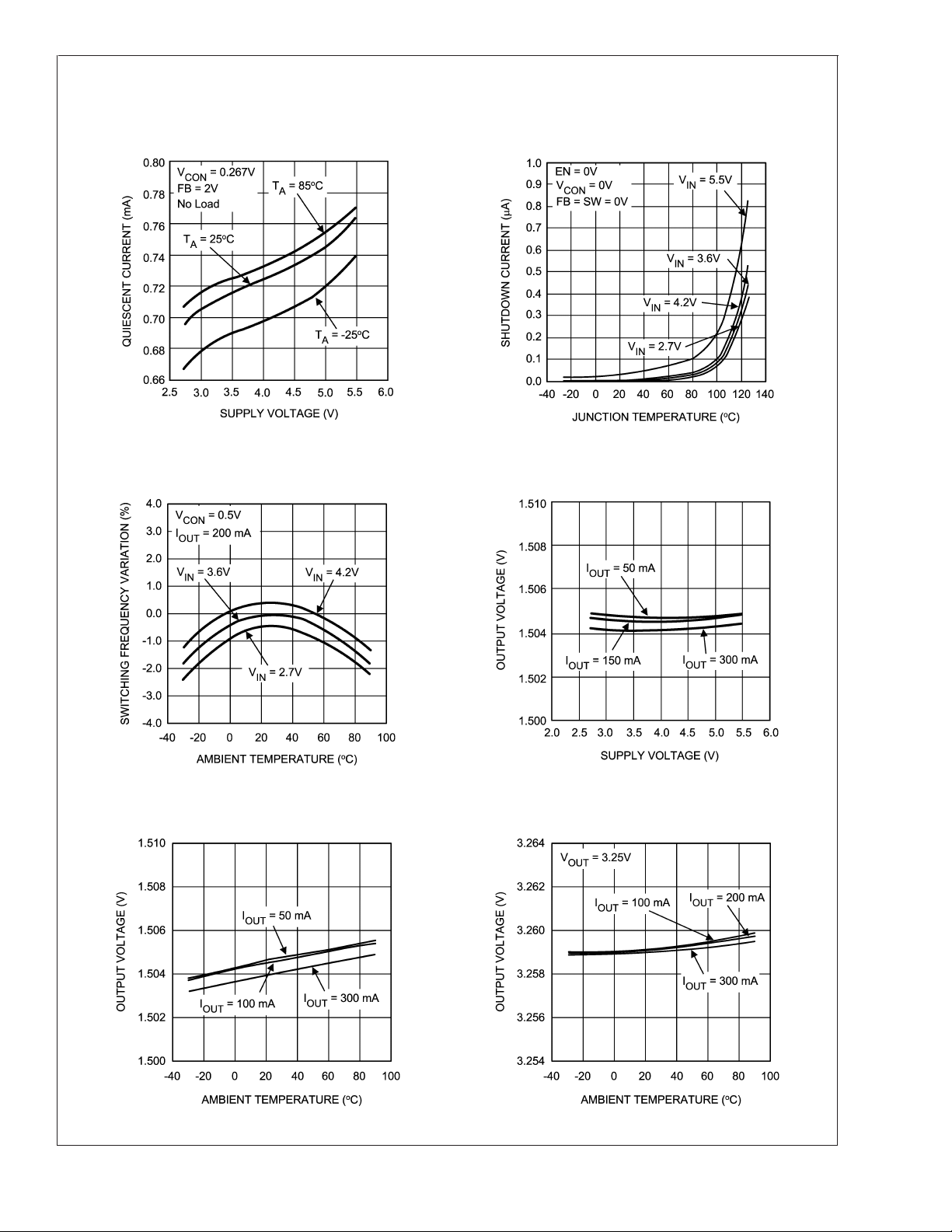
Typical Performance Characteristics (Circuit in Figure 1,PV
IN=VDD
= EN = 3.6V, BYP = 0V, TA=
25˚C, unless otherwise noted)
Quiescent Supply Current vs Supply Voltage Shutdown Supply Current vs Temperature
(EN = 0V)
20126104
Switching Frequency Variation vs Temperature
(V
OUT
= 1.5V, I
OUT
= 200 mA)
Output Voltage vs Supply Voltage
(V
= 1.5V)
OUT
20126105
Output Voltage vs Temperature
= 1.5V)
(V
OUT
20126106
20126107
Output Voltage vs Temperature
(V
= 3.25V)
OUT
20126108 20126109
www.national.com5

Typical Performance Characteristics (Circuit in Figure 1,PV
25˚C, unless otherwise noted) (Continued)
LM3200
Open/Closed Loop Current Limit vs Temperature
(PWM Mode)
IN=VDD
= EN = 3.6V, BYP = 0V, TA=
Output Voltage vs Output Current
(BYP Mode, V
= BYP = 3.6V)
IN
V
Voltage vs Output Voltage
CON
(I
OUT
= 200 mA)
20126112
Low V
20126114 20126115
Voltage vs Output Voltage
CON
(R
LOAD
=15Ω)
20126113
www.national.com 6

LM3200
Typical Performance Characteristics (Circuit in Figure 1,PV
25˚C, unless otherwise noted) (Continued)
Output Voltage vs Input Voltage
(BYP = 0V, Auto-Bypass Function)
Efficiency vs Output Current
= 1.5V)
(V
OUT
20126116
Efficiency vs Output Voltage
Efficiency vs Output Current
IN=VDD
(V
(V
OUT
= EN = 3.6V, BYP = 0V, TA=
= 3.9V)
IN
20126117
= 3.25V)
Load Transient Response
= 1.5V)
(V
OUT
20126118 20126119
Load Transient Response
(V
= 3.25V)
OUT
20126120 20126121
www.national.com7

Typical Performance Characteristics (Circuit in Figure 1,PV
25˚C, unless otherwise noted) (Continued)
LM3200
Startup
(V
= 3.6V, V
IN
= 1.5V, 15Ω)
OUT
20126122 20126123
IN=VDD
Shutdown Response
(VIN= 4.2V, V
OUT
= EN = 3.6V, BYP = 0V, TA=
= 3.25V, 15Ω)
Automatic Bypass Operation
= 4.2V to 3.0V)
(V
IN
Line Transient Response
= 3.0V to 3.6V)
(V
IN
Forced Bypass Operation
(VIN= 3.0V)
20126124 20126125
V
Voltage Response
CON
(V
IN
= 4.2V, V
= 0.5V/1.1V)
CON
20126126 20126127
www.national.com 8

LM3200
Typical Performance Characteristics (Circuit in Figure 1,PV
25˚C, unless otherwise noted) (Continued)
Timed Current Limit Response
(V
= 3.6V)
IN
20126128 20126129
Output Voltage Ripple
= 3.25V)
(V
OUT
Output Voltage Ripple in Dropout
(VIN= 3.57V, V
IN=VDD
= EN = 3.6V, BYP = 0V, TA=
Output Voltage Ripple
(V
= 1.5V)
OUT
= 3.25V, I
OUT
LOAD
= 200 mA)
R
vs Temperature
DSON
(P-ch)
20126130 20126131
R
vs Temperature
DSON
(N-ch)
20126132 20126133
www.national.com9

Typical Performance Characteristics (Circuit in Figure 1,PV
25˚C, unless otherwise noted) (Continued)
LM3200
R
vs Temperature
DSON
(Bypass FET)
IN=VDD
= EN = 3.6V, BYP = 0V, TA=
Dropout Voltage vs Output Current
(Bypass Mode)
Block Diagram
20126134
20126141
Operation Description
The LM3200 is a simple, step-down DC-DC converter with a
bypass switch, optimized for powering RF power amplifiers
(PAs) in mobile phones, portable communicators, and similar
battery powered RF devices. It is designed to allow the RF
PA to operate at maximum efficiency over a wide range of
power levels from a single Li-Ion battery cell. It is based on
www.national.com 10
20126135
current-mode buck architecture, with synchronous rectification for high efficiency. It is designed for a maximum load
capability of 300 mA in PWM mode and 500 mA in bypass
mode. Maximum load range may vary from this depending
on input voltage, output voltage and the inductor chosen.
The device has three-pin selectable operating modes required for powering RF PAs in mobile phones and other

Operation Description (Continued)
sophisticated portable device with complex power management needs. Fixed-frequency PWM operation offers regulated output at high efficiency while minimizing interference
with sensitive IF and data acquisition circuits. Bypass mode
(Forced or Automatic) turns on an internal FET bypass
switch to power the PA directly from the battery. Shutdown
mode turns the device off and reduces battery consumption
to 0.1 µA (typ).
DC PWM mode output voltage precision is +/-2% for
3.6V
load with 3.2V output, 3.6V input. PWM mode quiescent
current is 0.7 mA typ. The output voltage is dynamically
programmable from 0.8V to 3.6V by adjusting the voltage on
the control pin without the need for external feedback resistors. This ensures longer battery life by being able to change
the PA supply voltage dynamically depending on its transmitting power.
. Efficiency is typically around 96% for a 120 mA
OUT
LM3200
Additional features include current overload protection, over
voltage protection and thermal shutdown.
The LM3200 is constructed using a chip-scale 10-pin micro
SMD package. This package offers the smallest possible
size, for space-critical applications such as cell phones,
where board area is an important design consideration. Use
of a high switching frequency (2 MHz) reduces the size of
external components. As shown in Figure 1, only few external components are required for implementation. Use of a
micro SMD package requires special design considerations
for implementation. (See Micro SMD Package Assembly and
use in the Applications Information section.) Its fine bumppitch requires careful board design and precision assembly
equipment. Use of this package is best suited for opaquecase applications, where its edges are not subject to highintensity ambient red or infrared light. Also, the system controller should set EN low during power-up and other low
supply voltage conditions. (See Shutdown Mode in the Device Information section.)
FIGURE 1. Typical Operating System Circuit
Circuit Operation
Referring to Figure 1, the LM3200 operates as follows. During the first part of each switching cycle, the control block in
the LM3200 turns on the internal PFET (P-channel MOSFET) switch. This allows current to flow from the input
through the inductor to the output filter capacitor and load.
The inductor limits the current to a ramp with a slope of
around (V
During the second part of each cycle, the controller turns the
PFET switch off, blocking current flow from the input, and
then turns the NFET (N-channel MOSFET) synchronous
rectifier on. In response, the inductor’s magnetic field collapses, generating a voltage that forces current from ground
through the synchronous rectifier to the output filter capacitor
and load. As the stored energy is transferred back into the
circuit and depleted, the inductor current ramps down with a
slope around V
charge when the inductor current is going high, and releases
it when inductor current is going low, smoothing the voltage
across the load.
The output voltage is regulated by modulating the PFET
switch on time to control the average current sent to the load.
The effect is identical to sending a duty-cycle modulated
rectangular wave formed by the switch and synchronous
)/L, by storing energy in a magnetic field.
IN-VOUT
/L. The output filter capacitor stores
OUT
20126136
rectifier at SW to a low-pass filter formed by the inductor and
output filter capacitor. The output voltage is equal to the
average voltage at the SW pin.
PWM Mode
While in PWM (Pulse Width Modulation) mode, the output
voltage is regulated by switching at a constant frequency
and then modulating the energy per cycle to control power to
the load. Energy per cycle is set by modulating the PFET
switch on-time pulse width to control the peak inductor current. This is done by comparing the signal from the PFET
drain current to a slope-compensated reference current generated by the error amplifier. At the beginning of each cycle,
the clock turns on the PFET switch, causing the inductor
current to ramp up. When the current sense signal ramps
past the error amplifier signal, the PWM comparator turns off
the PFET switch and turns on the NFET synchronous rectifier, ending the first part of the cycle. If an increase in load
pulls the output down, the error amplifier output increases,
which allows the inductor current to ramp higher before the
comparator turns off the PFET. This increases the average
current sent to the output and adjusts for the increase in the
load. Before appearing at the PWM comparator, a slope
www.national.com11

PWM Mode (Continued)
compensation ramp from the oscillator is subtracted from the
LM3200
error signal for stability of the current feedback loop. The
minimum on-time of PFET in PWM mode is 50 ns (typ).
Bypass Mode
The LM3200 contains an internal PFET switch for bypassing
the PWM DC-DC converter during Bypass mode. In Bypass
mode, this PFET is turned on to power the PA directly from
the battery for maximum RF output power. When the part
operates in the Bypass mode, the output voltage will be the
input voltage less the voltage drop across the resistance of
the bypass PFET. Bypass mode is more efficient than operating in PWM mode at 100% duty cycle because the resistance of the bypass PFET is less than the series resistance
of the PWM PFET and inductor. This translates into higher
voltage available on the output in Bypass mode, for a given
battery voltage. The part can be placed in bypass mode by
sending BYP pin high. This is called Forced Bypass Mode
and it remains in bypass mode until BYP pin goes low.
Alternatively the part can go into Bypass mode automatically.
This is called Auto-bypass mode or Automatic Bypass mode.
The bypass switch turns on when the difference between the
input voltage and programmed output voltage is less than
250 mV (typ.) for more than the bypass delay time of 15 µs
(typ.). The bypass switch turns off when the input voltage is
higher than the programmed output voltage by 450 mV (typ.)
for longer than the bypass delay time. The bypass delay time
is provided to prevent false triggering into Automatic Bypass
mode by either spikes or dips in V
system resource friendly in that the Bypass PFET is turned
on automatically when the input voltage gets close to the
output voltage, typical scenario of a discharging battery. It is
also turned off automatically when the input voltage rises,
typical scenario of a charger connected. Another scenario
could be changes made to V
PFET to turn on and off automatically. It is recommended to
connect BYPOUT pin directly to the output capacitor with a
separate trace and not to the FB pin.
. This method is very
IN
voltage causing Bypass
CON
Operating Mode Selection Control
The BYP digital input pin is used to select between PWM/
Auto-bypass and Bypass operating mode. Setting BYP pin
>
1.2V) places the device in Forced Bypass mode.
high (
Setting BYP pin low (
device in PWM/Auto-bypass mode.
Bypass and PWM operation overlap during the transition
between the two modes. This transition time is approximately 31 µs when changing from PWM to Bypass mode,
and 15 µs when changing from Bypass to PWM mode. This
helps prevent under or overshoots during the transition period between PWM and Bypass modes.
<
0.4V) or leaving it floating places the
Shutdown Mode
Setting the EN digital pin low (<0.4V) places the LM3200 in
a 0.1 µA (typ.) Shutdown mode. During shutdown, the PFET
switch, NFET synchronous rectifier, reference voltage
source, control and bias circuitry of the LM3200 are turned
off. Setting EN high (
EN should be set low to turn off the LM3200 during power-up
and under voltage conditions when the power supply is less
than the 2.7V minimum operating voltage. The LM3200 is
designed for compact portable applications, such as mobile
phones. In such applications, the system controller deter-
>
1.2V) enables normal operation.
mines power supply sequencing and requirements for small
package size outweigh the benefit of including UVLO (Under
Voltage Lock-Out) circuitry.
Dynamically Adjustable Output Voltage
The LM3200 features dynamically adjustable output voltage
to eliminate the need for external feedback resistors. The
output can be set from 0.8V to 3.6V by changing the voltage
on the analog V
tions where peak power is needed only when the handset is
far away from the base station or when data is being transmitted. In other instances, the transmitting power can be
reduced. Hence the supply voltage to the PA can be reduced, promoting longer battery life. See Setting the Output
Voltage in the Application Information section for further
details.
pin. This feature is useful in PA applica-
CON
Over Voltage Protection
The LM3200 has an over voltage comparator that prevents
the output voltage from rising too high. If the output voltage
rises to 330 mV over its target, the OVP comparator inhibits
PWM operation to skip pulses until the output voltage returns
to the target. Typically the OVP comparator may be activated
during V
voltage. During the over voltage protection mode, both the
PWM PFET and the NFET synchronous rectifier are off.
When the part comes out of the over voltage protection
mode, the NFET synchronous rectifier remains off for approximately 3.5 µs to avoid inductor current going negative.
steps particularly steps from a high to a low
CON
Internal Synchronous Rectification
While in PWM mode, the LM3200 uses an internal NFET as
a synchronous rectifier to reduce rectifier forward voltage
drop and associated power loss. Synchronous rectification
provides a significant improvement in efficiency whenever
the output voltage is relatively low compared to the voltage
drop across an ordinary rectifier diode.
With medium and heavy loads, the internal NFET synchronous rectifier is turned on during the inductor current down
slope in the second part of each cycle. The synchronous
rectifier is turned off prior to the next cycle. There is no zero
cross detect, which means that the NFET can conduct current in both directions and inductor current is always continuous. The advantage of this method is that the part remains in PWM mode at light loads or no load conditions. The
NFET has a current limit. The NFET is designed to conduct
through its intrinsic body diode during transient intervals
before it turns on, eliminating the need for an external diode.
Current Limiting
A current limit feature allows the LM3200 to protect itself and
external components during overload conditions. In PWM
mode, a 940 mA (max.) cycle-by-cycle current limit is normally used. If an excessive load pulls the output voltage
down to below approximately 0.375V, indicating a possible
short to ground, then the device switches to a timed current
limit mode. In timed current limit mode, the internal PFET
switch is turned off after the current comparator trips, and the
beginning of the next cycle is inhibited for 3.5 µs to force the
instantaneous inductor current to ramp down to a safe value.
After the 3.5 µs interval, the internal PFET is turned on
again. This cycle is repeated until the load is reduced and
the output voltage exceeds approximately 0.375V. There-
www.national.com 12

LM3200
Current Limiting (Continued)
fore, the device may not startup if an excessive load is
connected to the output when the device is enabled. The
synchronous rectifier is off in the timed current limit mode.
Timed current limit prevents the loss of current control seen
in some products when the output voltage is pulled low in
serious overload conditions.
A current limit is also provided for the NFET. This is approximately −500 mA. Both the NFET and the PFET are turned off
in negative current limit until the PFET is turned on again at
the beginning of the next cycle. The negative current limit
inhibits buildup of excessive inductor current. In the Bypass
mode, the bypass current limit is 1000 mA(typ). The output
voltage drops when the bypass current limit kicks in.
Thermal Overload Protection
The LM3200 has a thermal overload protection function that
operates to protect the device from short-term misuse and
overload conditions. When the junction temperature exceeds
around 150˚C, the device inhibits operation. Both the PFET
and the NFET are turned off in PWM mode, and the Bypass
PFET is turned off in Bypass mode. When the temperature
drops below 130˚C, normal operation resumes. Prolonged
operation in thermal overload conditions may damage the
device and is considered bad practice.
Application Information
SETTING THE OUTPUT VOLTAGE
The LM3200 features a pin-controlled variable output voltage to eliminate the need for external feedback resistors. It
can be programmed for an output voltage from 0.8V to 3.6V
by setting the voltage on the V
formula:
=3xV
V
OUT
When V
is between 0.267V and 1.20V, the output volt-
CON
age will follow proportionally by 3 times of V
If V
is over 1.20V (V
CON
OUT
tion may occur because of insufficient slope compensation.
voltage is less than 0.267V (V
If V
CON
voltage may not be regulated due to the required on-time
being less than the minimum on-time (50ns). The output
voltage can go lower than 0.8V providing a limited V
is used. Refer to datasheet curve (Low V
Output Voltage) for details. This curve is for a typical part and
there could be part to part variation for output voltages less
than 0.8V over the limited V
IN
less than approx. 0.15V, the LM3200 output is turned off, but
the internal bias circuits are still active.
INDUCTOR SELECTION
A 2.2 µH inductor with saturation current rating over 940 mA
is recommended for almost all applications. The inductor
resistance should be less than 0.3Ω for better efficiency.
Table 1 lists suggested inductors and suppliers.
TABLE 1. Suggested Inductors and Their Suppliers
Model Size (WxLxH) [mm] Vendor
DO3314-222MX 3.3 x 3.3 x 1.4 Coilcraft
VLF3010AT-2R2M1R0 2.6 x 2.8 x 1.0 TDK
MIPW3226D2R2M 3.2 x 2.6 x 1.0 FDK
pin, as in the following
CON
CON
.
CON
= 3.6V), sub-harmonic oscilla-
= 0.8V), the output
OUT
range
IN
Voltage vs
CON
range. In addition, if V
CON
Model Size (WxLxH) [mm] Vendor
LPO3310-222MX 3.3 x 3.3 x 1.0 Coilcraft
If a higher value inductor is used the LM3200 may become
unstable and exhibit large under or over shoot during line,
load and V
transients. If smaller inductance value is
CON
used, slope compensation maybe insufficient causing subharmonic oscillations. The device has been tested with inductor values in the range 1.55µH to 3.1µH to account for
inductor tolerances.
For low-cost applications, an unshielded bobbin inductor can
be used. For noise-critical applications, an unshielded or
shielded-bobbin inductor should be used. A good practice is
to layout the board with footprints accommodating both
types for design flexibility. This allows substitution of an
unshielded inductor, in the event that noise from low-cost
bobbin models is unacceptable. Saturation occurs when the
magnetic flux density from current through the windings of
the inductor exceeds what the inductor’s core material can
support with a corresponding magnetic field. This can cause
poor efficiency, regulation errors or stress to a DC-DC converter like the LM3200.
CAPACITOR SELECTION
The LM3200 is designed to be used with ceramic capacitors.
Use a 10 µF ceramic capacitor for the input and a 4.7 µF
ceramic capacitor for the output. Ceramic capacitors such as
X5R, X7R and B are recommended for both filters. These
provide an optimal balance between small size, cost, reliability and performance for cell phones and similar applications.
Table 2 lists suggested capacitors and suppliers.
TABLE 2. Suggested Capacitors and Their Suppliers
Model Vendor
LMK212BJ475MG Taiyo-Yuden
C2012X5R1A475K TDK
GRM188R61A475K Murata
C3216X5R1A106K TDK
The DC bias characteristics of the capacitor must be considered when making the selection. If smaller case size such as
0603 is selected, the dc bias could reduce the cap value by
as much as 40%, in addition to the 20% tolerances and 15%
temperature coefficients. Request dc bias curves from
manufacturer when making selection.The device has been
designed to be stable with output capacitors as low as 3 µF
is
to account for capacitor tolerances.This value includes dc
bias reduction, manufacturing tolerences and temp coefficients.
The input filter capacitor supplies AC current drawn by the
PFET switch of the LM3200 in the first part of each cycle and
reduces the voltage ripple imposed on the input power
source. The output filter capacitor absorbs the AC inductor
current, helps maintain a steady output voltage during transient load changes and reduces output voltage ripple. These
capacitors must be selected with sufficient capacitance and
sufficiently low ESR (Equivalent Series Resistance) to perform these functions. The ESR of the filter capacitors is
generally a major factor in voltage ripple.
MICRO SMD PACKAGE ASSEMBLY AND USE
Use of the Micro SMD package requires specialized board
layout, precision mounting and careful re-flow techniques, as
detailed in National Semiconductor Application Note 1112.
www.national.com13

Application Information (Continued)
Refer to the section Surface Mount Technology (SMD) As-
LM3200
sembly Considerations. For best results in assembly, alignment ordinals on the PC board should be used to facilitate
placement of the device. The pad style used with Micro SMD
package must be the NSMD (non-solder mask defined) type.
This means that the solder-mask opening is larger than the
pad size. This prevents a lip that otherwise forms if the
solder-mask and pad overlap, from holding the device off the
surface of the board and interfering with mounting. See
Application Note 1112 for specific instructions how to do this.
The 10-Bump package used for the LM3200 has 300 micron
solder balls and requires 10.82 mil pads for mounting on the
circuit board. The trace to each pad should enter the pad
with a 90˚ entry angle to prevent debris from being caught in
deep corners. Initially, the trace to each pad should be 6-7
mil wide, for a section approximately 6 mil long or longer, as
a thermal relief. Then each trace should neck up or down to
its optimal width. The important criterion is symmetry. This
ensures the solder bumps on the LM3200 re-flow evenly and
that the device solders level to the board. In particular,
special attention must be paid to the pads for bumps B3, C3
and D3. Because PGND and PV
large copper planes, inadequate thermal relief can result in
inadequate re-flow of these bumps.
The Micro SMD package is optimized for the smallest possible size in applications with red or infrared opaque cases.
Because the Micro SMD package lacks the plastic encapsulation characteristic of larger devices, it is vulnerable to light.
Backside metalization and/or epoxy coating, along with frontside shading by the printed circuit board, reduce this sensitivity. However, the package has exposed die edges. In
particular, Micro SMD devices are sensitive to light, in the
red and infrared range, shining on the package’s exposed
die edges.
Do not use or power-up the LM3200 while subjecting it to
high intensity red or infrared light; otherwise degraded, unpredictable or erratic operation may result. Examples of light
sources with high red or infrared content include the sun and
halogen lamps. Place the device in a case opaque to red or
infrared light.
BOARD LAYOUT CONSIDERATIONS
PC board layout is an important part of DC-DC converter
design. Poor board layout can disrupt the performance of a
DC-DC converter and surrounding circuitry by contributing to
EMI, ground bounce, and resistive voltage loss in the traces.
These can send erroneous signals to the DC-DC converter,
resulting in poor regulation or instability. Poor layout can also
result in re-flow problems leading to poor solder joints between the Micro SMD package and board pads. Poor solder
joints can result in erratic or degraded performance. Good
layout for the LM3200 can by implemented by following a
few simple design rules.
are typically connected to
IN
1. Place the LM3200 on 10.82 mil pads. As a thermal relief,
connect to each pad with a 7 mil wide, approximately 7
mil long traces, and when incrementally increase each
trace to its optimal width. The important criterion is symmetry to ensure the solder bumps on the LM3200 re-flow
evenly (see Micro SMD Package Assembly and Use).
2. Place the LM3200, inductor and filter capacitors close
together and make the trace short. The traces between
these components carry relatively high switching currents and act as antennas. Following this rule reduces
radiated noise. Place the capacitors and inductor close
to the LM3200. The input capacitor should be placed
right next to the device between PV
and PGND pin.
IN
3. Arrange the components so that the switching current
loops curl in the same direction. During the first half of
each cycle, current flows from the input filter capacitor,
through the LM3200 and inductor to the output filter
capacitor and back through ground, forming a current
loop. In the second half of each cycle, current is pulled
up from ground, through the LM3200 by the inductor, to
the output filter capacitor and then back through ground,
forming a second current loop. Routing these loops so
the current curls in the same direction, prevents magnetic field reversal between the two half-cycles and reduces radiated noise.
4. Connect the ground pins of the LM3200, and filter capacitors together using generous component side copper fill as a pseudo-ground plane. Then connect this to
the ground-plane (if one is used) with several vias. This
reduces ground plane noise by preventing the switching
currents from circulating through the ground plane. It
also reduces ground bounce at the LM3200 by giving it
a low impedance ground connection.
5. Use wide traces between the power components and for
power connections to the DC-DC converter circuit. This
reduces voltage errors caused by resistive losses across
the traces.
6. Route noise sensitive traces, such as the voltage feedback trace, away from noisy traces and components.
The voltage feedback trace must remain close to the
LM3200 circuit and should be routed directly from FB pin
to V
at the output capacitor. A good approach is to
OUT
route the feedback trace on another layer and to have a
ground plane between the top layer and the layer on
which the feedback trace is routed. This reduces EMI
radiation on to the DC-DC converter’s own voltage feedback trace.
7. It is recommended to connect BYPOUT pin to V
OUT
the output capacitor using a separate trace, instead of
connecting it directly to the FB pin for better noise
immunity.
at
www.national.com 14

Physical Dimensions inches (millimeters) unless otherwise noted
LM3200 Miniature, Adjustable, Step-Down DC-DC Converter with Bypass Mode for RF Power
Amplifiers
10-Bump Thin Micro SMD, Large Bump
±
X1 = 1.819mm
X2 = 2.174mm
X3 = 0.600mm
0.030mm
±
0.030mm
±
0.075mm
NS Package Number TLP10NHA
National does not assume any responsibility for use of any circuitry described, no circuit patent licenses are implied and National reserves
the right at any time without notice to change said circuitry and specifications.
For the most current product information visit us at www.national.com.
LIFE SUPPORT POLICY
NATIONAL’S PRODUCTS ARE NOT AUTHORIZED FOR USE AS CRITICAL COMPONENTS IN LIFE SUPPORT DEVICES OR SYSTEMS
WITHOUT THE EXPRESS WRITTEN APPROVAL OF THE PRESIDENT AND GENERAL COUNSEL OF NATIONAL SEMICONDUCTOR
CORPORATION. As used herein:
1. Life support devices or systems are devices or systems
which, (a) are intended for surgical implant into the body, or
(b) support or sustain life, and whose failure to perform when
properly used in accordance with instructions for use
2. A critical component is any component of a life support
device or system whose failure to perform can be reasonably
expected to cause the failure of the life support device or
system, or to affect its safety or effectiveness.
provided in the labeling, can be reasonably expected to result
in a significant injury to the user.
BANNED SUBSTANCE COMPLIANCE
National Semiconductor certifies that the products and packing materials meet the provisions of the Customer Products Stewardship
Specification (CSP-9-111C2) and the Banned Substances and Materials of Interest Specification (CSP-9-111S2) and contain no ‘‘Banned
Substances’’ as defined in CSP-9-111S2.
National Semiconductor
Americas Customer
Support Center
Email: new.feedback@nsc.com
Tel: 1-800-272-9959
www.national.com
National Semiconductor
Europe Customer Support Center
Fax: +49 (0) 180-530 85 86
Email: europe.support@nsc.com
Deutsch Tel: +49 (0) 69 9508 6208
English Tel: +44 (0) 870 24 0 2171
Français Tel: +33 (0) 1 41 91 8790
National Semiconductor
Asia Pacific Customer
Support Center
Email: ap.support@nsc.com
National Semiconductor
Japan Customer Support Center
Fax: 81-3-5639-7507
Email: jpn.feedback@nsc.com
Tel: 81-3-5639-7560
 Loading...