

October 17, 2008
LM3151/LM3152/LM3153
SIMPLE SWITCHER® CONTROLLER, 42V Synchronous
Step-Down
LM3151/LM3152/LM3153 SIMPLE SWITCHER
General Description
The LM3151/2/3 SIMPLE SWITCHER® Controller is an easy
to use and simplified step down power controller capable of
providing up to 12A of output current in a typical application.
Operating with an input voltage range of 6V-42V, the
LM3151/2/3 features a fixed output voltage of 3.3V, and features switching frequencies of 250 kHz, 500 kHz, and 750
kHz. The synchronous architecture provides for highly efficient designs. The LM3151/2/3 controller employs a Constant
On-Time (COT) architecture with a proprietary Emulated Ripple Mode (ERM) control that allows for the use of low ESR
output capacitors, which reduces overall solution size and
output voltage ripple. The Constant On-Time (COT) regulation architecture allows for fast transient response and requires no loop compensation, which reduces external component count and reduces design complexity.
Fault protection features such as thermal shutdown, undervoltage lockout, over-voltage protection, short-circuit protection, current limit, and output voltage pre-bias startup allow for
a reliable and robust solution.
The LM3151/2/3 SIMPLE SWITCHER® concept provides for
an easy to use complete design using a minimum number of
external components and National’s WEBENCH® online design tool. WEBENCH® provides design support for every step
of the design process and includes features such as external
component calculation with a new MOSFET selector, electrical simulation, thermal simulation, and Build-It boards for
prototyping.
Features
PowerWise® step-down controller
■
6V to 42V Wide input voltage range
■
Fixed output voltage of 3.3V
■
Fixed switching frequencies of 250 kHz/500 kHz/750 kHz
■
No loop compensation required
■
Fully WEBENCH® enabled
■
Low external component count
■
Constant On-Time control
■
Ultra-Fast transient response
■
Stable with low ESR capacitors
■
Output voltage pre-bias startup
■
Valley current limit
■
Programmable soft-start
■
Typical Applications
Telecom
■
Networking Equipment
■
Routers
■
Security Surveillance
■
Power Modules
■
®
CONTROLLER, 42V Synchronous Step-Down
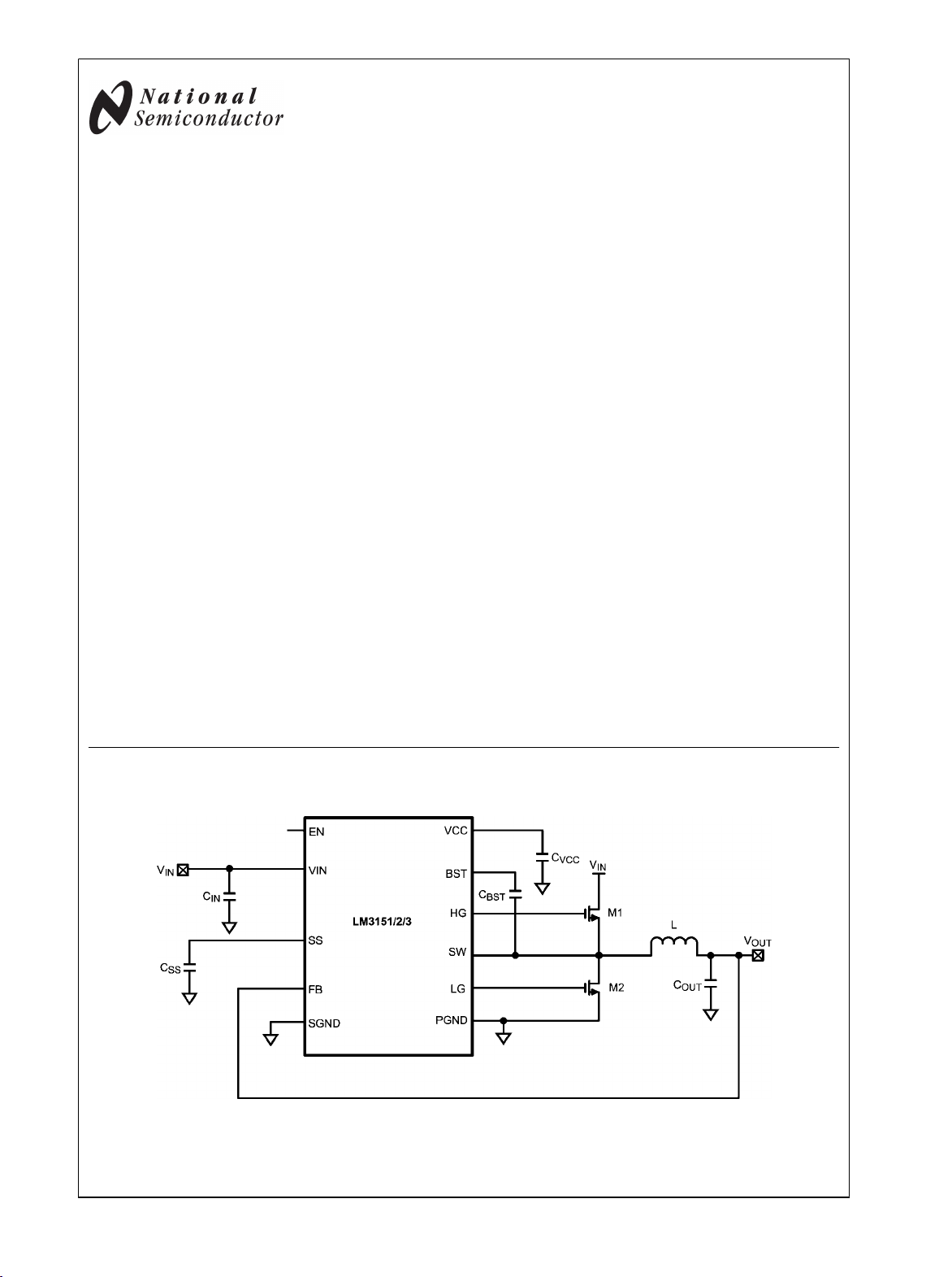
Typical Application
30053201
SIMPLE SWITCHER® is a registered trademark of National Semiconductor Corporation
© 2008 National Semiconductor Corporation 300532 www.national.com
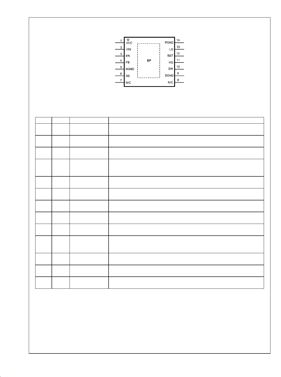
Connection Diagram
LM3151/LM3152/LM3153
Pin Descriptions
Pin Name Description Function
1 VCC
2 VIN Input Supply Voltage
3 EN Enable
4 FB Feedback
5,9 SGND Signal Ground
6 SS Soft-Start
7,8 N/C Not Connected
10 SW Switch Node
11 HG
12 BST
13 LG Low-Side Gate Drive
14 PGND Power Ground
EP EP Exposed Pad
Supply Voltage for
FET Drivers
High-Side Gate
Drive
Connection for
Bootstrap Capacitor
Nominally regulated to 5.95V. Connect a 1 µF to 2.2 µF decoupling capacitor from this
pin to ground.
Supply pin to the device. Nominal input range is 6V to 42V. See ordering information
for Vin limitations.
To enable the IC apply a logic high signal to this pin greater than 1.26V typical or leave
floating. To disable the part, ground the EN pin.
Internally connected to the resistor divider network which sets the fixed output voltage.
This pin also senses the output voltage faults such a over-voltage and short circuit
conditions.
Ground for all internal bias and reference circuitry. Should be connected to PGND at a
single point.
An internal 7.7 µA current source charges an external capacitor to provide the soft-start
function.
Internally not electrically connected. These pins may be left unconnected or connected
to ground.
Switch pin of controller and high-gate driver lower supply rail. A boost capacitor is also
connected between this pin and BST pin
Gate drive signal to the high-side NMOS switch. The high-side gate driver voltage is
supplied by the differential voltage between the BST pin and SW pin.
High-gate driver upper supply rail. Connect a 0.33 µF-0.47 µF capacitor from SW pin to
this pin. An internal diode charges the capacitor during the high-side switch off-time. Do
not connect to an external supply rail.
Gate drive signal to the low-side NMOS switch. The low-side gate driver voltage is
supplied by VCC.
Synchronous rectifier MOSFET source connection. Tie to power ground plane. Should
be tied to SGND at a single point.
Exposed die attach pad should be connected directly to SGND. Also used to help
dissipate heat out of the IC.
eTSSOP-14
30053202
www.national.com 2
Ordering Information
LM3151/LM3152/LM3153
Order Number Package Type NSC Package
Drawing
LM3151MH-3.3
LM3151MHE-3.3 250 Units in Tape and
LM3151MHX-3.3 2500 Units in Tape and
LM3152MH-3.3
LM3152MHE-3.3 250 Units in Tape and
LM3152MHX-3.3 2500 Units in Tape and
LM3153MH-3.3
LM3153MHE-3.3 250 Units in Tape and
LM3153MHX-3.3 2500 Units in Tape and
LM3151MH-2.5
LM3151MHE-2.5
LM3151MHX-2.5
LM3152MH-2.5
LM3152MHX-2.5
LM3153MH-2.5
LM3153MHX-2.5
LM3151MH-5.0
LM3151MHX-5.0
LM3152MH-5.0
LM3152MHX-5.0
LM3153MH-5.0
LM3153MHX-5.0
eTSSOP-14 MXA14A 6V - 42V 3.3V 250KHz
eTSSOP-14 MXA14A 6V - 33V 3.3V 500KHz
eTSSOP-14 MXA14A 8V - 18V 3.3V 750KHz
eTSSOP-14 MXA14A
eTSSOP-14 MXA14A
Input
Voltage
Range
*
* 500KHzLM3152MHE-2.5
* 750KHzLM3153MHE-2.5
*
* 500KHzLM3152MHE-5.0
* 750KHzLM3153MHE-5.0
Output
Voltage
2.5V
5.0V
Switching
Frequency
250KHz
250KHzLM3151MHE-5.0
Supplied As
94 Units per Anti-Static
Tube
Reel
Reel
94 Units per Anti-Static
Tube
Reel
Reel
94 Units per Anti-Static
Tube
Reel
Reel
*Coming Soon
3 www.national.com
Absolute Maximum Ratings (Note 1)
If Military/Aerospace specified devices are required,
please contact the National Semiconductor Sales Office/
All Other Inputs to GND -0.3V to 7V
ESD Rating (Note 2) 2kV
Storage Temperature Range -65°C to +150°C
Distributors for availability and specifications.
VIN to GND -0.3V to 47V
SW to GND -3V to 47V
BST to SW -0.3V to 7V
BST to GND -0.3V to 52V
LM3151/LM3152/LM3153
Electrical Characteristics Limits in standard type are for T
Operating Ratings (Note 1)
V
IN
Junction Temperature Range (TJ)
EN 0V to 5V
= 25°C only; limits in boldface type apply over the
J
−40°C to + 125°C
junction temperature (TJ) range of -40°C to +125°C. Minimum and Maximum limits are guaranteed through test, design, or statistical
correlation. Typical values represent the most likely parametric norm at TJ = 25°C, and are provided for reference purposes only.
Unless otherwise stated the following conditions apply: VIN = 18V.
Symbol Parameter Conditions Min Typ Max Units
Start-Up Regulator, VCC
V
CC
VIN - V
I
VCCL
VCC
UVLO
V
CC-UVLO-HYS
t
CC-UVLO-D
I
IN
I
IN-SD
CC
VIN - VCC Dropout Voltage
VCC Current Limit (Note 3) VCC = 0V 65 100
VCC Under-voltage Lockout threshold
(UVLO)
VCC UVLO Hysteresis
VCC UVLO Filter Delay
Input Operating Current No Switching
Input Operating Current, Device
Shutdown
C
= 1 µF, 0 mA to 40 mA 5.65 5.95 6.25
VCC
I
= 2 mA, Vin = 5.5V 40
VCC
I
= 30 mA, Vin = 5.5V 330
VCC
VCC Increasing
VCC Decreasing
4.75 5.1 5.40
475
3
3.6 5.2
VEN = 0V
32 55
GATE Drive
I
Q-BST
R
DS-HG-Pull-Up
R
DS-HG-Pull-Down
R
DS-LG-Pull-Up
R
DS-LG-Pull-Down
Boost Pin Leakage
HG Drive Pull–Up On-Resistance
HG Drive Pull–Down On-Resistance
LG Drive Pull–Up On-Resistance
LG Drive Pull–Down On-Resistance
V
– VSW = 6V 2
BST
IHG Source = 200 mA 5
IHG Sink = 200 mA 3.4
ILG Source = 200 mA 3.4
ILG Sink = 200 mA 2
Soft-Start
I
SS
I
SS-DIS
SS Pin Source Current
SS Pin Discharge Current
VSS = 0V 5.9 7.7 9.5
200
Current Limit
V
CL
Current Limit Voltage Threshold
175 200 225
ON/OFF Timer
t
ON-MIN
t
OFF
ON Timer Minimum Pulse Width
OFF Timer Minimum Pulse Width
200
370 525
Enable Input
V
V
EN-HYS
EN
EN Pin Input Threshold Trip Point
EN Pin threshold Hysteresis
VEN Rising 1.14 1.20 1.26
VEN Falling 120
6V to 42V
V
mV
mA
V
mV
µs
mA
µA
nA
Ω
Ω
Ω
Ω
mA
µA
mV
ns
ns
V
mV
www.national.com 4
Symbol Parameter Conditions Min Typ Max Units
Boost Diode
I
= 2 mA 0.7
V
f
Forward Voltage
BST
I
= 30 mA 1
BST
V
V
Thermal Characteristics
T
SD
θ
JA
Thermal Shutdown Rising 165 °C
Thermal Shutdown Hysteresis Falling 15 °C
Junction to Ambient
4 Layer JEDEC Printed Circuit
Board, 9 Vias, No Air Flow
2 Layer JEDEC Printed Circuit
40
140
°C/W
Board. No Air Flow
θ
JC
Junction to Case No Air Flow
4
°C/W
3.3V Output Option
Symbol Parameter Conditions Min Typ Max Units
V
V
OUT-OV
OUT
Output Voltage
Output Voltage Over-Voltage Threshold
3.234 3.3 3.366
3.83 4.00 4.17
V
V
LM3151-3.3 42
V
IN-MAX
Maximum Input Voltage (Note 4)
VLM3152-3.3 33
LM3153-3.3 18
LM3151-3.3 6
V
IN-MIN
Minimum Input Voltage (Note 4)
VLM3152-3.3 6
LM3153-3.3 8
LM3151-3.3, RON = 115 kΩ
f
S
Switching Frequency
LM3152-3.3, RON = 51 kΩ
LM3153-3.3, RON = 32 kΩ
LM3151-3.3, RON = 115 kΩ
t
ON
On-Time
LM3152-3.3, RON = 51 kΩ
LM3153-3.3, RON = 32 kΩ
R
FB
FB Resistance to Ground
250
500
750
730
400
330
566
kHz
ns
kΩ
LM3151/LM3152/LM3153
Note 1: Absolute Maximum Ratings indicate limits beyond which damage to the device may occur. Operating Ratings indicate conditions for which the device is
intended to be functional, but does not guarantee specific performance limits. For guaranteed specifications and conditions, see the Electrical Characteristics.
Note 2: The human body model is a 100 pF capacitor discharged through a 1.5 kΩ resistor into each pin. Test Method is per JESD-22-A114.
Note 3: VCC provides self bias for the internal gate drive and control circuits. Device thermal limitations limit external loading.
Note 4: The input voltage range is dependent on minimum on-time, off-time, and therefore frequency, and is also affected by optimized MOSFET selection.
5 www.national.com
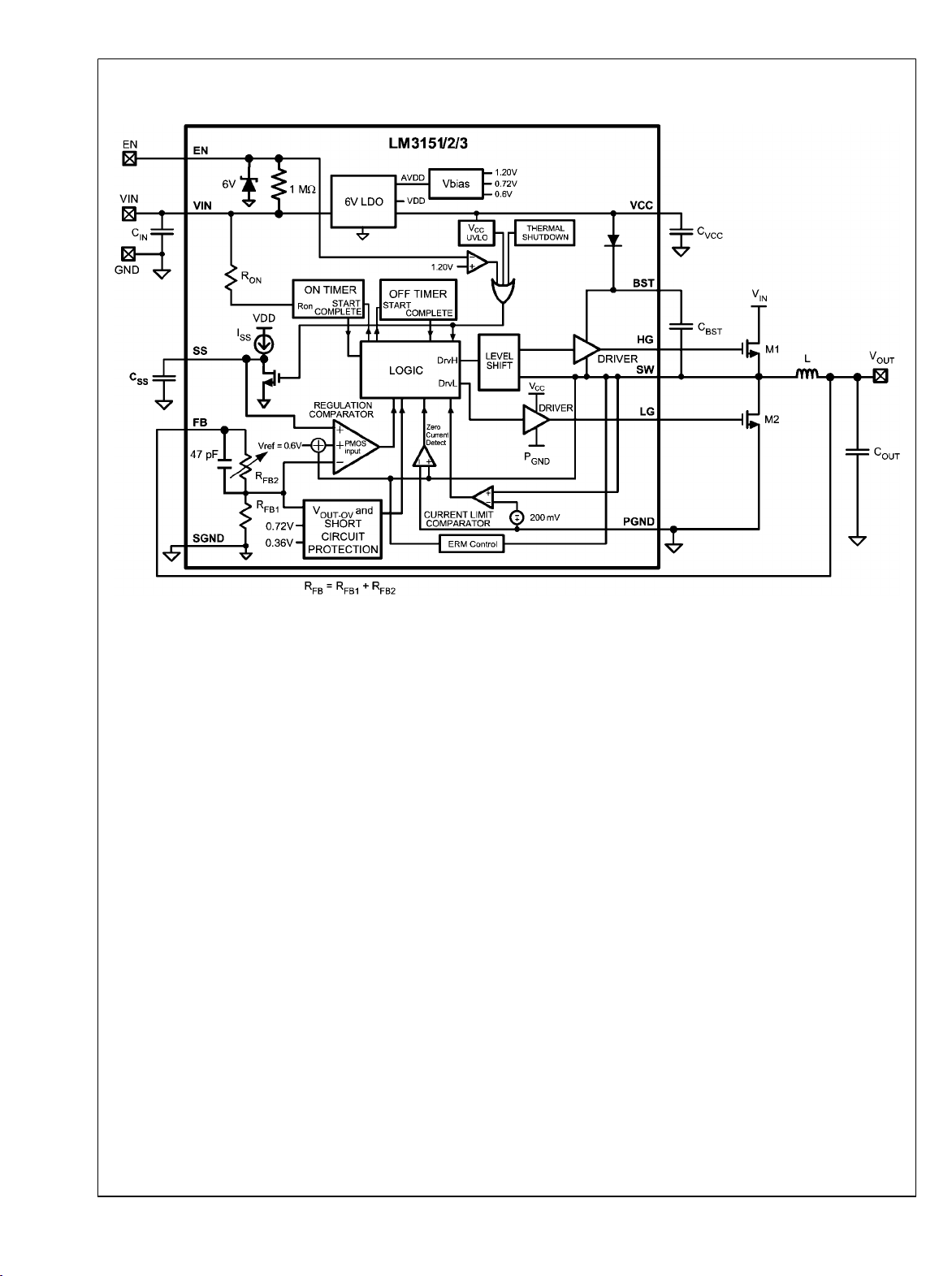
Simplified Block Diagram
LM3151/LM3152/LM3153
30053203
www.national.com 6
 Loading...