

查询LM3089供应商
LM3089 FM Receiver IF System
General Description
The LM3089 has been designed to provide all the major
functions required for modern FM IF designs of automotive,
high-fidelity and communications receivers.
Features
Y
Three stage IF amplifier/limiter provides 12 mV (typ)
b
3 dB limiting sensitivity
Y
Balanced product detector and audio amplifier provide
400 mV (typ) of recovered audio with distortion as low
as 0.1% with proper external coil designs.
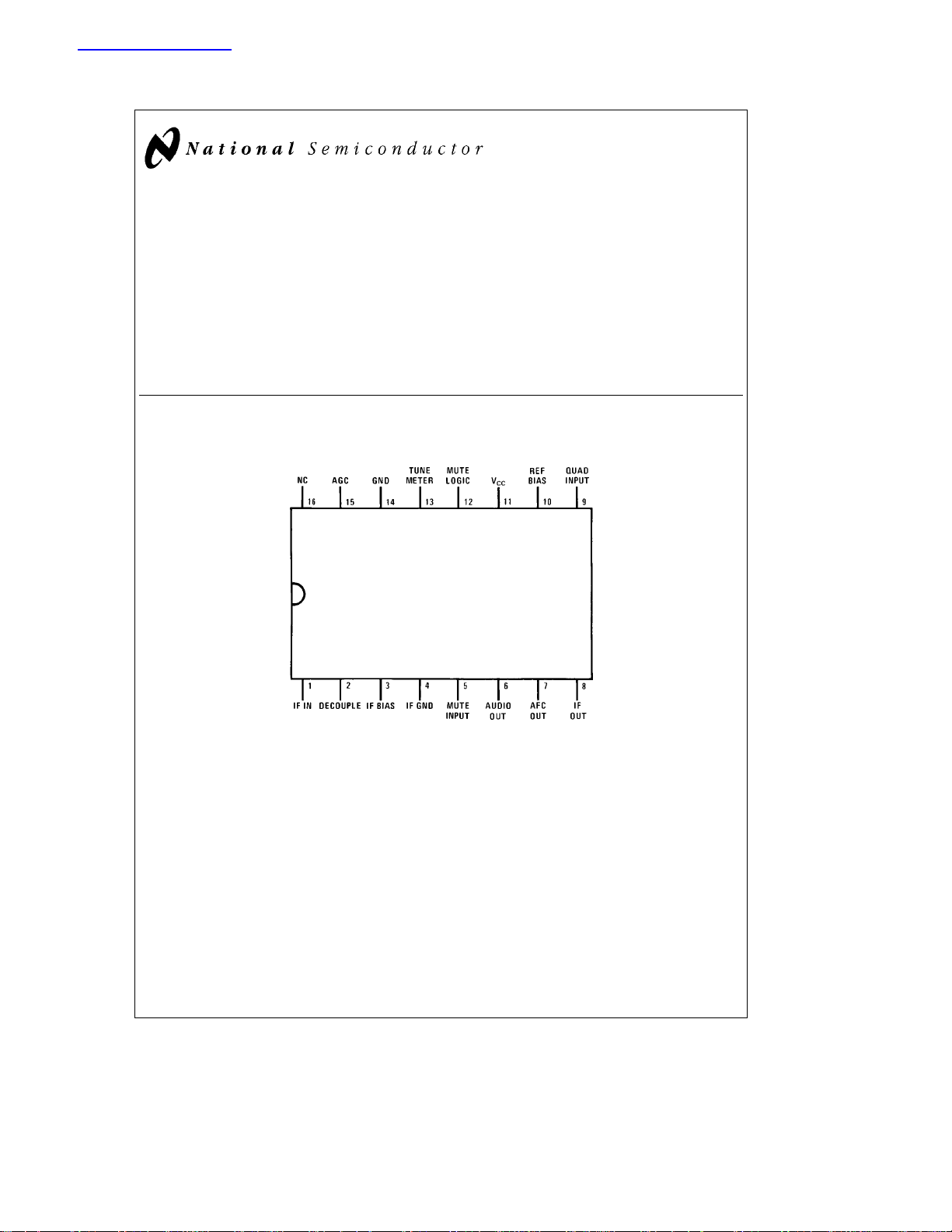
Connection Diagram
Y
Four internal carrier level detectors provide delayed
AGC signal to tuner, IF level meter drive current and interchannel mute control
Y
AFC amplifier provides AFC current for tuner and/or
center tuning meters
Y
Improved operating and temperature performance, especially when using high Q quadrature coils in narrow
band FM communications receivers
Y
No mute circuit latchup problems
Y
A direct replacement for CA3089E
Dual-In-Line Package
LM3089 FM Receiver IF System
September 1992
Top View
TL/H/7149– 2
Order Number LM3089N
See NS Package Number N16E
C
1995 National Semiconductor Corporation RRD-B30M115/Printed in U. S. A.
TL/H/7149

Block Diagram
TL/H/7149– 1
Toko America
1250 Feehanville Drive
Mount Prospect, IL 60056
(312) 297-0070
2
Absolute Maximum Ratings
If Military/Aerospace specified devices are required,
please contact the National Semiconductor Sales
Office/Distributors for availability and specifications.
Supply Voltage Between Pin 11 and Pins 4, 14
DC Current Out of Pin 12 5 mA
DC Current Out of Pin 13 5 mA
DC Current Out of Pin 15 2 mA
a
16V
Power Dissipation (Note 2) 1500 mW
Operating Temperature Range
Storage Temperature Range
b
40§Ctoa85§C
b
65§Ctoa150§C
Lead Temperature
(Soldering, 10 seconds) 260
C
§
Electrical Characteristics (T
A
e
25§C, V
ea
12V, see Test Circuit)
CC
Symbol Parameter Conditions Min Typ Max Units
DC CHARACTERISTICS (V
I
11
V1, 2, 3 IF Input and Bias 1.2 1.9 2.4 V
Supply Current 16 23 30 mA
e
0, NOT MUTED)
IN
V6 Audio Output 5.0 5.6 6.0 V
V7 AFC Output 5.0 5.6 6.0 V
V10 Reference Bias 5.0 5.6 6.0 V
V12 Mute Control 5.0 5.4 6.0 V
V13 IF Level 0 0.5 V
V15 Delayed AGC 4.2 4.7 5.3 V
DYNAMIC CHARACTERISTICS f
e
10.7 MHZ, Df
o
e
g
75 kHz@400 Hz
VIN(LIM) Input Limitingb3dB 12 25 mV
AMR AM Rejection V
V
(AF) Recovered Audio V
O
THD Total Harmonic Distortion
Single Tuned (Note 1) V
Double Tuned (Note 1) V
a
S
N/N Signal to Noise Ratio V
V12 Mute Control V
V13 IF Level V
V13 IF Level V
V15 Delayed AGC V
V15 Delayed AGC V
V
(AF) Audio Muted V
O
Note 1: Distortion is a function of quadrature coil used.
Note 2: For operation in ambient temperatures above 25
C/W junction to ambient.
of 80
§
C, the device must be derated based on a 150§C maximum junction temperature and a thermal resistance
§
e
100 mV, AM: 30% 45 55
IN
e
10 mV 300 400 500 mVrms
IN
e
100 mV 0.5 1.0 %
IN
e
100 mV 0.1 0.3 %
IN
e
100 mV 60 70 dB
IN
e
100 mV 0 0.5 V
IN
e
100 mV 4.0 5.0 6.0 V
IN
e
500 mV 1.0 1.5 2.0 V
IN
e
100 mV 0.1 0.5 V
IN
e
30 mV 2.5 V
IN
e
100 mV, V5ea2.5V 60
IN
b
b
dB
dB
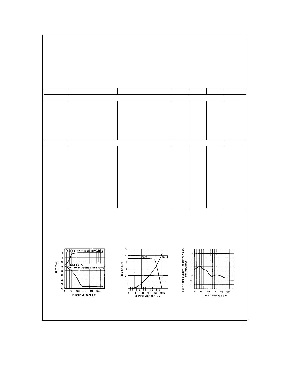
Typical Performance Characteristics
a
Typical S
N/N and IF Limiting
Sensitivity vs IF Input Signal
Typical AGC (Pin 15) and
Meter Output (Pin 13) vs
IF Input Signal
AM Rejection (30% Mod) vs
IF Input Signal
TL/H/7149– 3
3

Schematic Diagram
TL/H/7149– 4
4

Typical Performance Characteristics
Supply Current (I
Supply Voltage (V11)
11
Typical Audio Attenuation
(Pin 6) vs Mute Input
Voltage (Pin 5)
)vs
Reference Voltage, AGC and
Meter Output vs Supply Voltage
TL/H/7149– 6
Mute Control Output (Pin 12)
vs IF Input Signal
TL/H/7149– 5
DC Test Circuit
AC Test Circuit
KAC-K2318HM
TL/H/7149– 8
TL/H/7149– 7
*For single tuned dectector coil:
tunes with 100 pF at 10.7 MHz
L
O
(unloaded)j75
Q
UL
(loaded)j13 for V9j150 mVrms
Q
L
**For double tuned detector coil:
Q
ULPRIeQULSEC
kQj0.7 for V9j150 mVrms
Note:
The recovered audio output voltage will be approximately 0.5 dB less when
using the double tuned detector coil.
For proper operation of the mute circuit, the RF voltage at pin 9 should be
150 mVrms
g
30 mV.
j
75
5
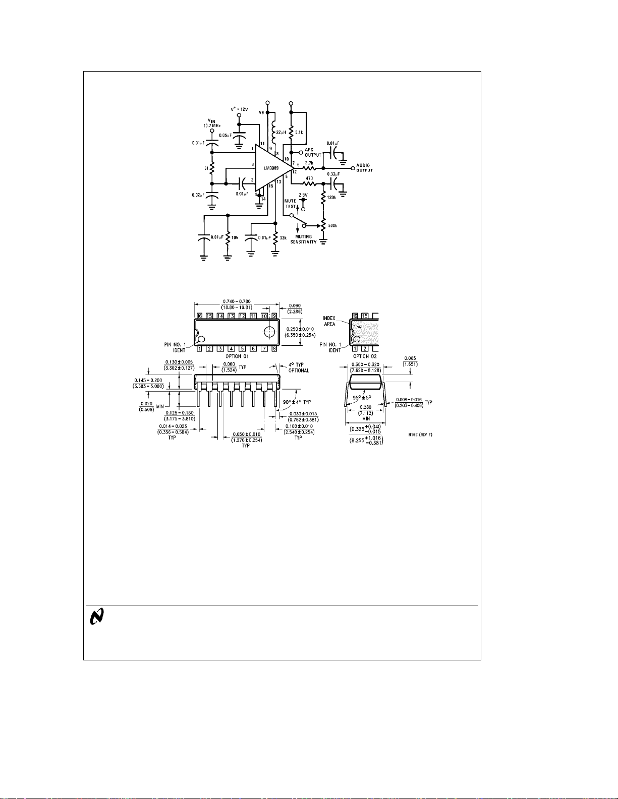
AC Test Circuit (Continued)
LM3089 FM Receiver IF System
TL/H/7149– 9
Physical Dimensions inches (millimeters)
Dual-In-Line Package (N)
Order Number LM3089N
See NS Package Number N16E
LIFE SUPPORT POLICY
NATIONAL’S PRODUCTS ARE NOT AUTHORIZED FOR USE AS CRITICAL COMPONENTS IN LIFE SUPPORT
DEVICES OR SYSTEMS WITHOUT THE EXPRESS WRITTEN APPROVAL OF THE PRESIDENT OF NATIONAL
SEMICONDUCTOR CORPORATION. As used herein:
1. Life support devices or systems are devices or 2. A critical component is any component of a life
systems which, (a) are intended for surgical implant support device or system whose failure to perform can
into the body, or (b) support or sustain life, and whose be reasonably expected to cause the failure of the life
failure to perform, when properly used in accordance support device or system, or to affect its safety or
with instructions for use provided in the labeling, can effectiveness.
be reasonably expected to result in a significant injury
to the user.
National Semiconductor National Semiconductor National Semiconductor National Semiconductor
Corporation Europe Hong Kong Ltd. Japan Ltd.
1111 West Bardin Road Fax: (
Arlington, TX 76017 Email: cnjwge@tevm2.nsc.com Ocean Centre, 5 Canton Rd. Fax: 81-043-299-2408
Tel: 1(800) 272-9959 Deutsch Tel: (
Fax: 1(800) 737-7018 English Tel: (
National does not assume any responsibility for use of any circuitry described, no circuit patent licenses are implied and National reserves the right at any time without notice to change said circuitry and specifications.
Fran3ais Tel: (
Italiano Tel: (
a
49) 0-180-530 85 86 13th Floor, Straight Block, Tel: 81-043-299-2309
a
49) 0-180-530 85 85 Tsimshatsui, Kowloon
a
49) 0-180-532 78 32 Hong Kong
a
49) 0-180-532 93 58 Tel: (852) 2737-1600
a
49) 0-180-534 16 80 Fax: (852) 2736-9960
 Loading...