


查询LM3075供应商
LM3075
High Efficiency, Synchronous Current Mode Buck
Controller
LM3075 High Efficiency, Synchronous Current Mode Buck Controller
September 2005
General Description
The LM3075 is a current mode control, synchronous buck
controller IC. Use of synchronous rectification and pulseskipping operation at light load achieves high efficiency over
a wide load range. Fixed frequency operation can be obtained by disabling the pulse-skipping mode. Current mode
control assures excellent line and load regulation and a wide
loop bandwidth for fast response to load transients.
Current mode control can be achieved by either sensing
across the high side NFET or a sense resistor. The switching
frequency can be selected as either 200 kHz or 300 kHz
from an internal clock.
The LM3075 is available with an adjustable output in a
TSSOP-20 package.
Typical Application Circuit
Features
n Input voltage range of 4.5V-36V
n Current Mode Control
n Skip mode operation available
n Cycle by cycle current limit
n 1.24V
±
2% Reference
Applications
n Automotive Power Supplies
n Distributed Power Systems
20162301
© 2005 National Semiconductor Corporation DS201623 www.national.com
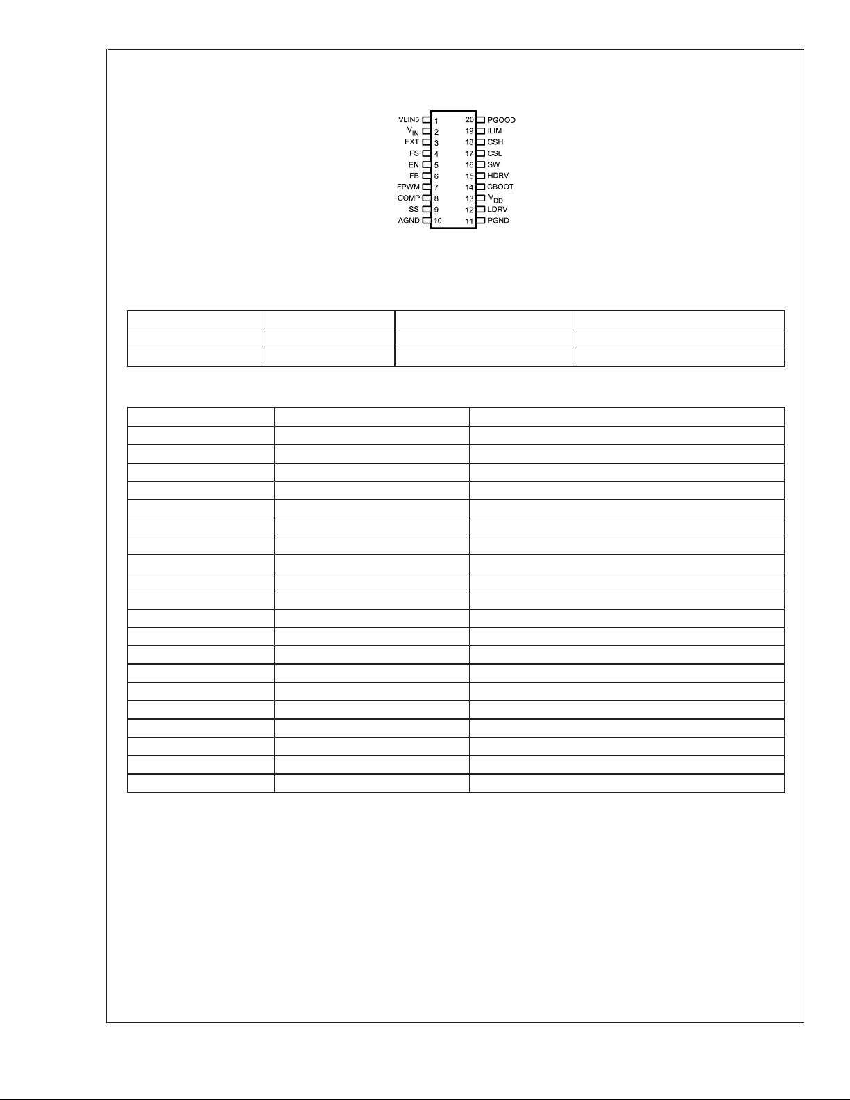
Connection Diagram
LM3075
TOP VIEW
20-Lead TSSOP (MTC)
20162302
Ordering Information
Order Number Package Type NSC Package Drawing Supplied As
LM3075MTC TSSOP-20 MTC-20 73 Units per Anti-Static Tube
LM3075MTCX TSSOP-20 MTC-20 2500 Units on Tape and Reel
Pin Descriptions
LM3075 Pin # Name Function
1 VLIN5 5V linear regulator output
2 VIN Input voltage supply
3 EXT External power connection for VLIN5
4 FS Frequency select
5 EN Enable pin
6 FB Feedback pin
7 FPWM Forced PWM selection
8 COMP Compensation pin
9 SS Output enable / soft-start pin
10 AGND Analog ground
11 PGND Power ground
12 LDRV Low side gate drive
13 VDD Low side gate drive supply
14 CBOOT Bootstrap capacitor connection
15 HDRV High side gate drive
16 SW Switch node
17 CSL Current sense low
18 CSH Current sense high
19 ILIM Current limit threshold adjustment
20 PGOOD Power good flag
www.national.com 2

LM3075
Absolute Maximum Ratings (Note 1)
If Military/Aerospace specified devices are required,
please contact the National Semiconductor Sales Office/
Distributors for availability and specifications.
Voltages from the indicated pins to GND:
VIN, ILIM, CSH −0.3V to 38V
SW, CSL −0.3 to (V
+ 0.3V)
IN
HDRV to SW −0.3V
HDRV to CBOOT +0.3V
Storage Temperature Range −65˚C to +150˚C
Junction Temperature 150˚C
Lead Temperature (Soldering, 10
sec) 260˚C
ESD Rating (Note 2) 1.5kV
PGOOD, FB, VDD, EXT, EN −0.3V to +7V
COMP, SS, FPWM, FS −0.3V to (V
LIN5
Operating Ratings(Note 1)
+0.3)V
CBOOT -0.3V to +43V
CBOOT to SW −0.3V to 7V
LDRV −0.3V to (V
DD
+0.3V)
Electrical Characteristics Limits in standard type are for T
over the junction temperature T
sign, or statistical correlation. Typical values represent the most likely parametric norm at T
erence purposes only. Unless otherwise specified V
range of -40˚C to +125˚C. Minimum and Maximum limits are guaranteed through test, de-
J
= 12V.
IN
Junction Temperature −40˚C to +125˚C
VIN to GND 4.5V to 36V
EXT 6V Max
= 25˚C only, and limits in boldface type apply
J
= 25˚C, and are provided for ref-
J
Symbol Parameter Conditions Min Typ Max Unit
V
FB
Feedback pin voltage VIN= 4.5V to 36V 1.213 1.238 1.259 V
Load Regulation V
= 0.5V to 1.5V 0.04 %
COMP
Line Regulation VIN= 4.5V to 36V 0.04 %
I
Q
I
SD
V
LIN5
V
UVLO
V
UVLO_HYS
V
CL_OS
I
ILIM
I
SS_SRC
I
SS_SNK
V
SS_TO
V
OVP
V
OVP_HYS
POWERGOOD
V
PWR_GOOD
V
PWR_BAD
T
PGOOD
I
OL
I
OH
GATE DRIVE
Operating Quiescent current VIN= 4.5V to 36V 1.0 2 mA
Shutdown Quiescent current VEN=0V 60 100 µA
V
Output Voltage I
LIN5
V
Under Voltage
LIN5
= 0 to 25mA V
VLIN5
V
= 5.5V to 36V 4.7 5 5.3
IN
3.7 3.9 4.1 V
Lockout
V
Under Voltage
LIN5
0.2 V
Lockout Hysteresis
Current Limit Comparator
±
0.2 mV
Offset
(V
ILIM–VCSL
I
sink current 8.3 10 11.3 µA
LIM
Soft-Start Pin Source
)
VSS= 1.2V 1 2 3 µA
Current
Soft-Start Pin Sink Current VSS=2V 4 µA
Soft-Start Timeout
2V
Threshold
Over Voltage Protection
With respect to V
FB
105 111 117 %
Rising Threshold
Over Voltage Protection
With respect to V
FB
2.8 %
Hysteresis
PGOOD Rising Threshold 92.5 95.5 98.5 %
PGOOD Falling Threshold 87 90.5 95 %
PGOOD delay PGOOD pin de-asserting 10 µs
PGOOD Low Sink Current V
PGOOD High Leakage
V
= 0.4V 0.6 1mA
PGOOD
=5V 5 200 nA
PGOOD
Current
www.national.com3
Electrical Characteristics Limits in standard type are for T
over the junction temperature T
LM3075
or statistical correlation. Typical values represent the most likely parametric norm at T
purposes only. Unless otherwise specified V
Symbol Parameter Conditions Min Typ Max Unit
I
CBOOT
R
ds_on 1
C
BOOT
HDRV FET driver pull-up
On resistance
R
ds_on 2
HDRV FET driver pull-down
On resistance
R
ds_on 3
LDRV FET driver pull-up On
resistance
R
ds_on 4
LDRV FET driver pull-down
On resistance
OSCILLATOR
f
D
T
ON_MIN
OSC
MAX
Oscillator Frequency VFS=5V 255 300 330 kHz
Maximum Dutycycle VFB=1V 95.5 98 %
Minimum On Time 180 260 ns
ERROR AMPLIFIER
I
FB
I
COMP_SRC
Feedback pin bias current VFB= 1.5V 50 nA
COMP Output Source
Current
I
COMP_SNK
COMP Output Sink Current VFB= 1.5V
Gm Error Amplifier
Transconductance
A
VOL
V
SL
Error Amplifier Voltage Gain 1250 V/V
Slope Compensation
(referred to the internal
summing node)
A
CS
Current Sense Amplifier
Gain
LOGIC
V
IL
FS, /FPWM Pin Maximum
Low Level Input Level
V
IH
FS, /FPWM Pin Minimum
High Level Input Level
THERMAL SHUTDOWN
T
T
SD_HYS
SD
Thermal Shutdown 160 ˚C
Thermal Shutdown
Hysteresis
EXT
R
TH
EXT
EXT
EXT pin on resistance V
VLIN5 to EXT Switch Over
Rising Threshold
range of -40˚C to +125˚C. Minimum and Maximum limits are guaranteed through test, design,
J
= 12V. (Continued)
IN
Leakage Current V
V
=7V 10 nA
CBOOT
=0V 165 200 215
FS
VFB=1V
=1V
V
COMP
= 0.5V
V
COMP
= 0V 0.051 V/µs
V
FS
= 5V 0.076
V
FS
V
= 1.25V 4 5 6 V/V
COMP
=5V
EXT
=50mA
I
VLIN5
= 25˚C only, and limits in boldface type apply
J
= 25˚C, and are provided for reference
J
2.9 Ω
1.7 Ω
2.4 Ω
0.8 Ω
120 µA
110 µA
620 µmho
0.8 V
2 V
10 ˚C
4 Ω
4.6 V
www.national.com 4

LM3075
Electrical Characteristics Limits in standard type are for T
over the junction temperature T
or statistical correlation. Typical values represent the most likely parametric norm at T
purposes only. Unless otherwise specified V
Note 1: Absolute maximum ratings indicate limits beyond which damage to the device may occur. Operating Range indicates conditions for which the device is
intended to be functional, but does not guarantee specfic performance limits. For guaranteed specifications and test conditions, see the Electrical Characteristics.
The guaranteed specifications apply only for the test conditions. Some performance characteristics may degrade when the device is not operated under the listed
test conditions.
Note 2: For testing purposes, ESD was applied using the human-body model, a 100pF capacitor discharged through a 1.5kΩ resistor.
range of -40˚C to +125˚C. Minimum and Maximum limits are guaranteed through test, design,
J
= 12V. (Continued)
IN
= 25˚C only, and limits in boldface type apply
J
= 25˚C, and are provided for reference
J
www.national.com5
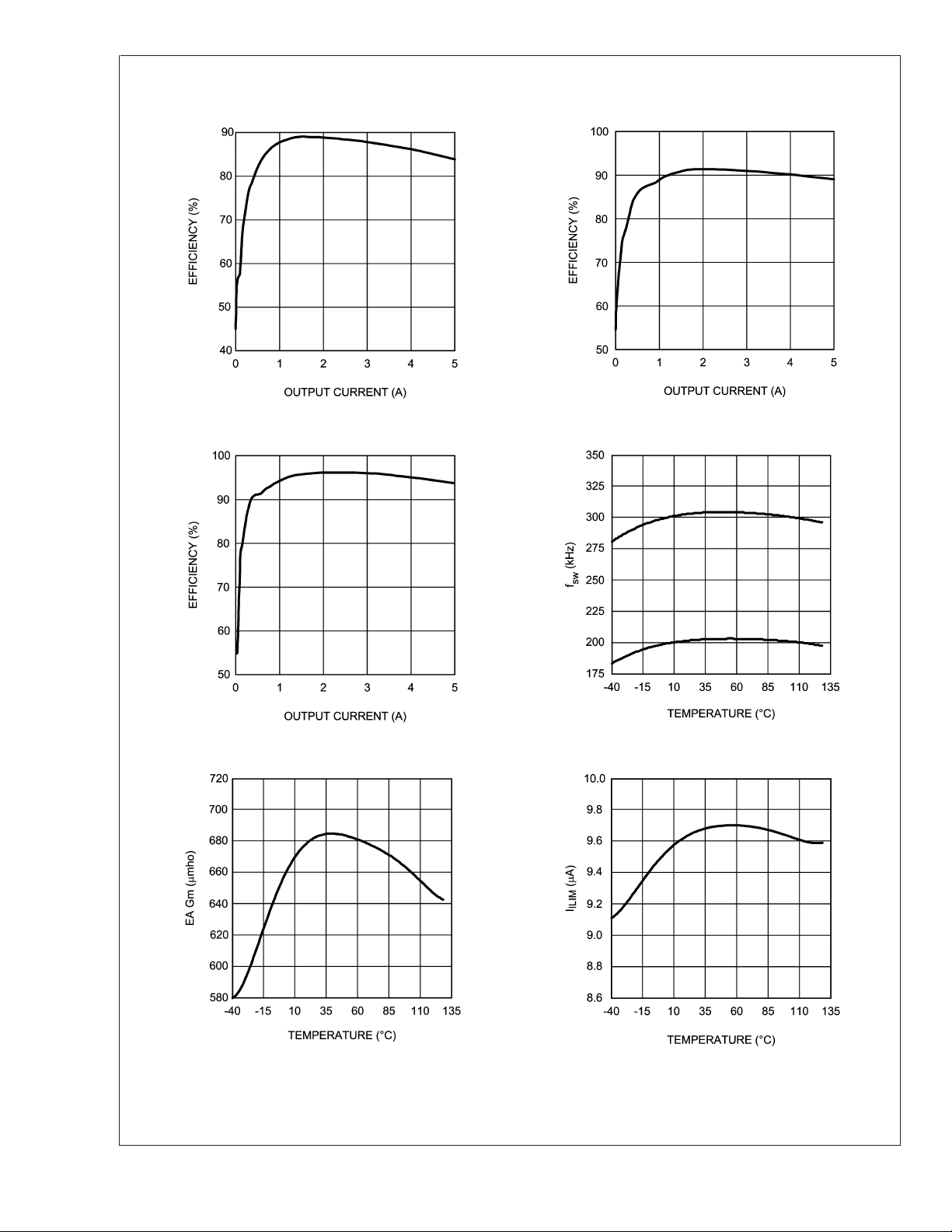
Typical Performance Characteristics
LM3075
Efficiency (VIN= 12V to V
= 1.8V) Efficiency (VIN= 12V to V
OUT
OUT
= 3.3V)
20162351
Efficiency (VIN= 12V to V
= 5V) Switching Frequency vs Temperature
OUT
20162362
Error Amplifier Gm vs Temperature ILIM vs Temperature
20162361
20162363
20162364
www.national.com 6
20162352
 Loading...