

查询LM3045供应商
LM3045/LM3046/LM3086 Transistor Arrays
LM3045/LM3046/LM3086 Transistor Arrays
December 1994
General Description
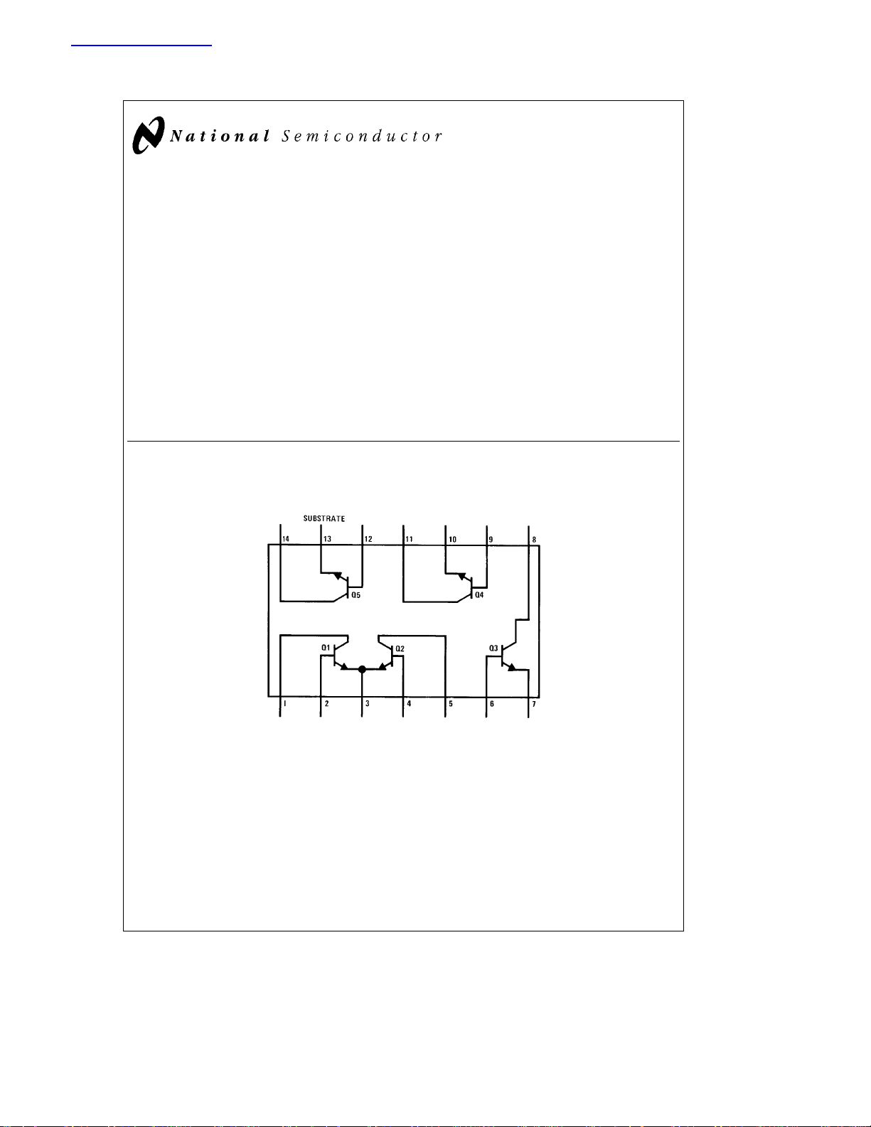
The LM3045, LM3046 and LM3086 each consist of five
general purpose silicon NPN transistors on a common
monolithic substrate. Two of the transistors are internally
connected to form a differentially-connected pair. The transistors are well suited to a wide variety of applications in low
power system in the DC through VHF range. They may be
used as discrete transistors in conventional circuits however, in addition, they provide the very significant inherent integrated circuit advantages of close electrical and thermal
matching. The LM3045 is supplied in a 14-lead cavity dualin-line package rated for operation over the full military temperature range. The LM3046 and LM3086 are electrically
identical to the LM3045 but are supplied in a 14-lead molded dual-in-line package for applications requiring only a limited temperature range.
Schematic and Connection Diagram
Dual-In-Line and Small Outline Packages
Features
Y
Two matched pairs of transistors
V
matchedg5mV
BE
Input offset current 2 mA max at I
Y
Five general purpose monolithic transistors
Y
Operation from DC to 120 MHz
Y
Wide operating current range
Y
Low noise figure 3.2 dB typ at 1 kHz
Y
Full military
temperature range (LM3045)
e
1mA
C
b
55§Ctoa125§C
Applications
Y
General use in all types of signal processing systems
operating anywhere in the frequency range from DC to
VHF
Y
Custom designed differential amplifiers
Y
Temperature compensated amplifiers
Top View
TL/H/7950– 1
Order Number LM3045J, LM3046M, LM3046N or LM3086N
See NS Package Number J14A, M14A or N14A
C
1995 National Semiconductor Corporation RRD-B30M115/Printed in U. S. A.
TL/H/7950
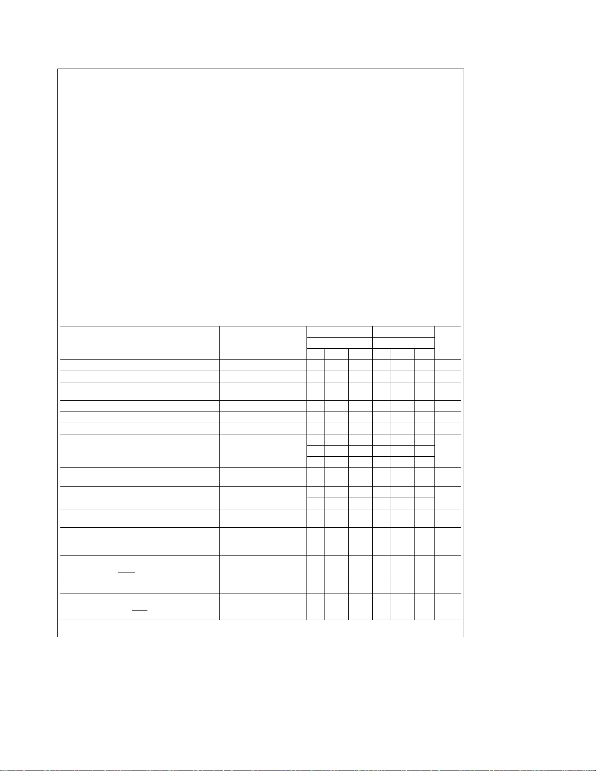
Absolute Maximum Ratings (T
If Military/Aerospace specified devices are required, please contact the National Semiconductor Sales Office/
Distributors for availability and specifications.
Power Dissipation:
e
T
25§C 300 750 300 750 mW
A
e
T
25§Cto55§C 300 750 mW
A
l
T
55§C Derate at 6.67 mW/§C
A
e
T
25§Cto75§C 300 750 mW
A
l
T
75§C Derate at 8 mW/§C
A
Collector to Emitter Voltage, V
Collector to Base Voltage, V
Collector to Substrate Voltage, V
Emitter to Base Voltage, V
Collector Current, I
Operating Temperature Range
Storage Temperature Range
Soldering Information
Dual-In-Line Package Soldering (10 Sec.) 260
Small Outline Package
Vapor Phase (60 Seconds) 215
Infrared (15 Seconds) 220
See AN-450 ‘‘Surface Mounting Methods and Their Effect on Product Reliability’’ for other methods of soldering surface mount
devices.
C
EBO
CEO
CBO
(Note 1) 20 20 V
CIO
Electrical Characteristics (T
Parameter Conditions LM3045, LM3046 LM3086 Units
Collector to Base Breakdown Voltage (V
Collector to Emitter Breakdown Voltage (V
Collector to Substrate Breakdown I
Voltage (V
Emitter to Base Breakdown Voltage (V
Collector Cutoff Current (I
Collector Cutoff Current (I
Static Forward Current Transfer V
Ratio (Static Beta) (hFE)
Input Offset Current for Matched V
Pair Q
and Q
1
Base to Emitter Voltage (VBE)V
Magnitude of Input Offset Voltage for V
Differential Pair
Magnitude of Input Offset Voltage for Isolated V
Transistors
b
V
l
BE5
Temperature Coefficient of Base to V
Emitter Voltage
Collector to Emitter Saturation Voltage (V
Temperature Coefficient of V
Input Offset Voltage
Note 1: The collector of each transistor of the LM3045, LM3046, and LM3086 is isolated from the substrate by an integral diode. The substrate (terminal 13) must
be connected to the most negative point in the external circuit to maintain isolation between transistors and to provide for normal transistor action.
(BR)CIO
l
V
BE3
)
)V
CBO
)V
CEO
b
I
I
l
2
V
l
V
BE3
l
O1
IO2
b
V
BE1
b
l
BE2
V
V
l,l
BE4
BE4
l
DV
BE
DT
#
J
DV
10
DT
#
J
(BR)CBO
(BR)CEO)IC
(BR)EBO
b
V
, 0.45 5 mV
l
BE5
CE(SAT)
e
25§C)
A
LM3045 LM3046/LM3086
Each Total Each Total Units
Transistor Package Transistor Package
15 15 V
20 20 V
55V
50 50 mA
b
55§Ctoa125§C
b
65§Ctoa150§C
C 260§C
§
e
25§C unless otherwise specified)
A
e
)I
C
e
e
C
)I
10 mA, I
E
CB
CE
CE
CE
CE
CE
CE
CE
e
)I
B
CE
10 mA, I
1 mA, I
10 mA, I
e
e
e
e
e
e
e
e
1 mA, I
e
e
E
e
0 1524 1524 V
B
e
CI
e
05757V
C
e
10V, I
E
e
10V, I
B
3V
3V, I
3V
3V, I
3V, I
3V, I
3V, I
e
I
C
e
I
C
e
I
C
e
1mA
C
e
I
E
Ð
e
I
E
e
1mA
C
e
1mA
C
e
1mA
C
e
10 mA 0.23 0.23 V
C
e
1mA
C
2
Min Typ Max Min Typ Max
0 2060 2060 V
0
0 0.002 40 0.002 100 nA
0 0.5 5 mA
1mA
10 mA
20 60 20 60 V
10 mA
1 mA 40 100 40 100
10 mAÐ
b
40§Ctoa85§C
b
65§Ctoa85§C
C
§
C
§
Limits Limits
100 100
54 54
0.3 2 mA
0.715 0.715
0.800 0.800
0.45 5 mV
b
1.9
1.1 mV/§C
b
1.9 mV/
V
C
§

Electrical Characteristics (Continued)
Parameter Conditions Min Typ Max Units
Low Frequency Noise Figure (NF) fe1 kHz, V
e
100 mA, R
I
C
CE
e
3V,
e
1kX
S
3.25 dB
LOW FREQUENCY, SMALL SIGNAL EQUIVALENT CIRCUIT CHARACTERISTICS
Forward Current Transfer Ratio (hfe)f
e
1 kHz, V
e
1 mA (LM3086)
I
C
e
3V, 110 (LM3045, LM3046)
CE
Short Circuit Input Impednace (hie) 3.5 kX
Open Circuit Output Impedance (hoe) 15.6 mmho
b
Open Circuit Reverse Voltage Transfer Ratio (hre) 1.8x10
4
ADMITTANCE CHARACTERISTICS
Forward Transfer Admittance (Yfe)f
Input Admittance (Yie)
e
1 MHz, V
e
I
1mA
C
e
3V, 31bj 1.5
CE
0.3
a
J 0.04
Output Admittance (Yoe) 0.001aj 0.03
Reverse Transfer Admittance (Yre) See Curve
e
Gain Bandwidth Product (fT)V
Emitter to Base Capacitance (CEB)V
Collector to Base Capacitance (CCB)V
Collector to Substrate Capacitance (CCI)V
CE
EB
CB
CS
e
3V, I
3 mA 300 550
C
e
e
3V, I
0 0.6 pF
E
e
e
3V, I
0 0.58 pF
C
e
e
3V, I
0 2.8 pF
C
Typical Performance Characteristics
Typical Collector To Base
Cutoff Current vs Ambient
Temperature for Each
Transistor
Typical Input Offset Current Offset Voltage for Differential
for Matched Transistor Pair
Q1Q2vs Collector Current
Typical Collector To Emitter
Cutoff Current vs Ambient
Temperature for Each
Transistor
Typical Static Base To Emitter
Voltage Characteristic and Input
Pair and Paired Isolated
Transistors vs Emitter Current
Typical Static Forward
Current-Transfer Ratio and
Beta Ratio for Transistors Q
and Q2vs Emitter Current
1
TL/H/7950– 2
TL/H/7950– 3
3

Typical Performance Characteristics (Continued)
Typical Base To Emitter
Voltage Characteristic for
Each Transistor vs Ambient
Temperature
Typical Noise Figure vs
Collector Current
Typical Input Offset Voltage
Characteristics for Differential
Pair and Paired Isolated
Transistors vs Ambient
Temperature
Typical Noise Figure vs
Collector Current
Typical Noise Figure vs
Collector Current
TL/H/7950– 4
Typical Normalized Forward
Current Transfer Ratio, Short
Circuit Input Impedance,
Open Circuit Output Impedance,
and Open Circuit Reverse
Voltage Transfer Ratio vs
Collector Current
Typical Forward Transfer
Admittance vs Frequency
Typical Input Admittance
vs Frequency
4
TL/H/7950– 5
Typical Output Admittance
vs Frequency
TL/H/7950– 6

Typical Performance Characteristics (Continued)
Typical Reverse Transfer
Admittance vs Frequency
Physical Dimensions inches (millimeters)
Typical Gain-Bandwidth
Product vs Collector Current
TL/H/7950– 7
Ceramic Dual-In-Line Package (J)
Order Number LM3045J
NS Package Number J14A
5

Physical Dimensions inches (millimeters) (Continued)
Molded Small Outline Package (M)
Order Number LM3046M
NS Package Number M14A
LM3045/LM3046/LM3086 Transistor Arrays
Molded Dual-In-Line Package (N)
Order Number LM3046N or LM3086N
NS Package Number N14A
LIFE SUPPORT POLICY
NATIONAL’S PRODUCTS ARE NOT AUTHORIZED FOR USE AS CRITICAL COMPONENTS IN LIFE SUPPORT
DEVICES OR SYSTEMS WITHOUT THE EXPRESS WRITTEN APPROVAL OF THE PRESIDENT OF NATIONAL
SEMICONDUCTOR CORPORATION. As used herein:
1. Life support devices or systems are devices or 2. A critical component is any component of a life
systems which, (a) are intended for surgical implant support device or system whose failure to perform can
into the body, or (b) support or sustain life, and whose be reasonably expected to cause the failure of the life
failure to perform, when properly used in accordance support device or system, or to affect its safety or
with instructions for use provided in the labeling, can effectiveness.
be reasonably expected to result in a significant injury
to the user.
National Semiconductor National Semiconductor National Semiconductor National Semiconductor
Corporation Europe Hong Kong Ltd. Japan Ltd.
1111 West Bardin Road Fax: (
Arlington, TX 76017 Email: cnjwge@tevm2.nsc.com Ocean Centre, 5 Canton Rd. Fax: 81-043-299-2408
Tel: 1(800) 272-9959 Deutsch Tel: (
Fax: 1(800) 737-7018 English Tel: (
National does not assume any responsibility for use of any circuitry described, no circuit patent licenses are implied and National reserves the right at any time without notice to change said circuitry and specifications.
Fran3ais Tel: (
Italiano Tel: (
a
49) 0-180-530 85 86 13th Floor, Straight Block, Tel: 81-043-299-2309
a
49) 0-180-530 85 85 Tsimshatsui, Kowloon
a
49) 0-180-532 78 32 Hong Kong
a
49) 0-180-532 93 58 Tel: (852) 2737-1600
a
49) 0-180-534 16 80 Fax: (852) 2736-9960
 Loading...