

Page 1
April 2, 2008
LM2854
4A 500 kHz / 1 MHz PowerWise® Synchronous SIMPLE
SWITCHER® Buck Regulator
LM2854 4A 500 kHz / 1 MHz PowerWise® Synchronous SIMPLE SWITCHER® Buck Regulator
General Description
The LM2854 PowerWise® SIMPLE SWITCHER® buck regulator is a 500 kHz or 1 MHz step-down switching voltage
regulator capable of driving up to a 4A load with exceptional
power conversion efficiency, line and load regulation, and
output accuracy. The LM2854 can accept an input voltage rail
between 2.95V and 5.5V and deliver an adjustable and highly
accurate output voltage as low as 0.8V. Externally established soft-start with a small capacitor facilitates controlled
start-up, and the LM2854 is capable of starting gracefully into
a pre-biased output voltage. Partial internal compensation reduces the number of external passive components and PC
board space typically necessary in a voltage mode buck converter application, yet preserving flexibility to deal with ceramic and/or electrolytic based load capacitors. Lossless
cycle-by-cycle peak current limit is used to protect the load
from an overcurrent or short-circuit fault, and an enable comparator simplifies sequencing applications. The LM2854 is
available in an exposed pad TSSOP-16 package that enhances the thermal performance of the regulator.
Features
Input voltage range of 2.95V to 5.5V
■
Maximum load current of 4A
■
Wide bandwidth voltage mode control loop, partial internal
■
compensation
Fixed switching frequency of 500 kHz or 1 MHz
■
35 mΩ integrated MOSFET switches
■
Adjustable output voltage down to 0.8V
■
Optimized reference voltage initial accuracy and
■
temperature drift
External soft-start control with tracking capability
■
Enable pin with hysteresis
■
Low standby current of 230 µA
■
Pre-biased load startup capability
■
Integrated UVLO, OCP and thermal shutdown
■
100% duty cycle capability
■
eTSSOP-16 exposed pad package
■
Applications
Low Voltage POL Regulation from 5V or 3.3V Rail
■
Local Solution for FPGA/DSP/ASIC/µP Core or I/O Power
■
Broadband Networking and Communications
■
Infrastructure
Portable Computing
■
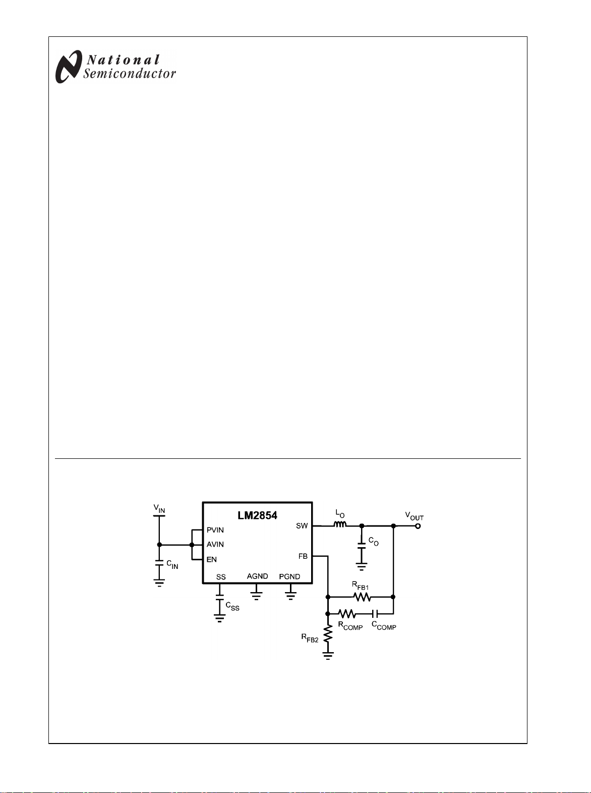
Typical Application Circuit
30052801
SIMPLE SWITCHER® is a Registered Trademark of National Semiconductor Corporation.
© 2008 National Semiconductor Corporation 300528 www.national.com
Page 2
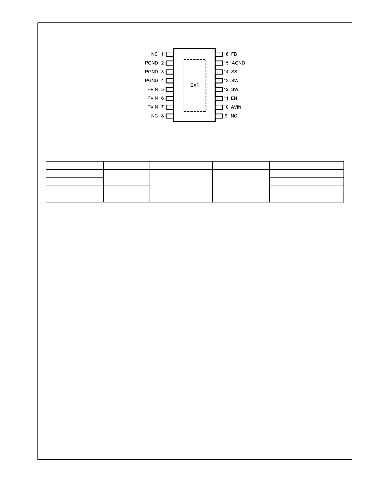
Connection Diagram
LM2854
Top View
16-Lead eTSSOP
30052802
Ordering Information
Order Number Frequency Package Type Package Drawing Supplied As
LM2854MH-500 500 kHz
LM2854MHX-500 2500 Units, Tape and Reel
LM2854MH-1000 1 MHz 92 Units, Rail
LM2854MHX-1000 2500 Units, Tape and Reel
TSSOP-16 exposed pad MXA16A
92 Units, Rail
www.national.com 2
Page 3
Pin Descriptions
Pin Number Name Description
1 NC Reserved for factory use, this pin should be connected to GND to ensure proper operation.
2,3,4 PGND Power ground pins for the internal power switches. These pins should be connected together locally
at the device and tied to the PC board ground plane.
5,6,7 PVIN Input voltage to the power switches inside the device. These pins should be connected together at the
device. A low ESR input capacitance should be located as close as possible to these pins.
8,9 NC Reserved for factory use, these pins should be connected to GND to ensure proper operation.
10 AVIN Analog input voltage supply that generates the internal bias. The UVLO circuit derives its input from
this pin also. Thus, if the voltage on AVIN falls below the UVLO threshold, both internal FETs are turned
off. It is recommended to connect PVIN to AVIN through a low pass RC filter to minimize the influence
of input rail ripple and noise on the analog control circuitry. The series resistor should be 1Ω and the
bypass capacitor should be a X7R ceramic type 0.1 µF to 1.0 µF.
11 EN Active high enable input for the device. Typically, turn-on threshold is 1.23V with 0.15V hysteresis. An
external resistor divider from PVIN can be used to effectively increase the UVLO turn-on threshold. If
not used, the EN pin should be connected to PVIN.
12,13 SW Switch node pins. This is the PWM output of the internal MOSFET power switches. These pins should
be tied together locally and connected to the filter inductor.
14 SS Soft-start control pin. An internal 2 µA current source charges an external capacitor connected between
this pin and AGND to set the output voltage ramp rate during startup. This pin can also be used to
configure the tracking feature.
15 AGND Quiet analog ground for the internal bias circuitry.
16 FB Feedback pin is connected to the inverting input of the voltage loop error amplifier. A 0.8V bandgap
reference is connected to the non-inverting input of the error amplifier.
EXP Exposed
Pad
Exposed metal pad on the underside of the package with a weak electrical connection to PGND. It is
recommended to connect this pad to the PC board ground plane in order to improve thermal
dissipation.
LM2854
3 www.national.com
Page 4
Absolute Maximum Ratings (Notes 1, 6)
If Military/Aerospace specified devices are required,
LM2854
please contact the National Semiconductor Sales Office/
Distributors for availability and specifications.
PVIN, AVIN, SW, EN, FB, SS to GND -0.3V to 6.0V
ESD Susceptibility (Note 2) ±2 kV
Power Dissipation Internally Limited
Junction Temperature 150°C
Storage Temperature Range −65°C to +150°C
Lead Temperature
Soldering (10 sec) 260°C
Vapor Phase (60 sec) 215°C
Infrared 220°C
Operating Ratings (Note 6)
PVIN to GND 2.95V to 5.5V
AVIN to GND 2.95V to 5.5V
Junction Temperature −40°C to +125°C
Electrical Characteristics Specifications with standard typeface are for T
= 25°C only; limits in bold face type
J
apply over the Operating Junction Temperature Range TJ range of -40°C to 125°C. Minimum and maximum limits are guaranteed
through test, design, or statistical correlation. Typical values represent the most likely parametric norm at TJ = 25°C, and are
provided for reference purposes only. AVIN = PVIN = EN = 5.0V, unless otherwise indicated in the Conditions column.
Symbol Parameter Conditions Min
(Note 3)
Typ
(Note 4)
Max
(Note 3)
SYSTEM PARAMETERS
ΔV
ΔV
V
REF
REF
V
REF
/ΔAVIN
/ΔI
ON
Reference Voltage (Note 5) Measured at the FB pin 0.790 0.8 0.808 V
Line Regulation (Note 5)
Load Regulation Normal operation 0.25 mV/A
O
ΔAVIN = 2.95V to 5.50V
0.04 0.6 %
UVLO Threshold (AVIN) Rising 2.6 2.95 V
Falling hysteresis 25 170 375 mV
R
DS(ON)-P
R
DS(ON)-N
I
SS
I
CL
I
I
SD
Q
PFET On Resistance ISW = 4A 35 65
NFET On Resistance ISW = 4A 34 65
Soft-Start Current 2 µA
Peak Current Limit Threshold 4.5 6.0 6.7 A
Operating Current Non-switching 1.7 3 mA
Shut Down Quiescent Current EN = 0V 230 500 µA
PWM SECTION
f
SW
Switching Frequency 1 MHz option 800 1050 1160 kHz
500 kHz option 400 525 580 kHz
D
range
PWM Duty Cycle Range 0 100 %
ENABLE CONTROL
V
V
EN(HYS)
IH
EN Pin Rising Threshold 0.8 1.23 1.65 V
EN Pin Hysteresis 150 mV
THERMAL CONTROL
T
T
SD-HYS
SD
TJ for Thermal Shutdown 165 °C
Hysteresis for Thermal Shutdown 10 °C
THERMAL RESISTANCE
θ
JA
Junction to Ambient MXA16A 35 °C/W
Units
mΩ
mΩ
Note 1: Absolute Maximum Ratings are limits beyond which damage to the device may occur. Operating Ratings are conditions under which operation of the
device is intended to be functional. For guaranteed specifications and test conditions, see the Electrical Characteristics.
Note 2: The human body model is a 100 pF capacitor discharged through a 1.5 kΩ resistor into each pin. Test method is per JESD22-AI14.
Note 3: Min and Max limits are 100% production tested at 25°C. Limits over the operating temperature range are guaranteed through correlation using Statistical
Quality Control (SQC) methods. Limits are used to calculate National’s Average Outgoing Quality Level (AOQL).
Note 4: Typical numbers are at 25°C and represent the most likely parametric norm.
Note 5: V
Note 6: PGND and AGND are electrically connected together on the PC board and the resultant net is termed GND.
www.national.com 4
measured in a non-switching, closed-loop configuration.
REF
Page 5

Typical Performance Characteristics Unless otherwise specified, the following conditions apply: VIN =
PVIN = AVIN = EN = 5.0V, CIN is 47 µF 10V X5R ceramic capacitor, LO is from TDK SPM6530T family; T
curves, bode plots and waveforms, and TJ = 25°C for all others.
= 25°C for efficiency
AMBIENT
LM2854
Feedback Voltage vs. Temperature
Soft Start Current vs Temperature
30052803
UVLO Threshold vs. Temperature
30052804
Enable Threshold vs. Temperature
30052805
Switching Frequency vs. Temperature
30052807
30052806
PMOS R
5 www.national.com
vs. Temperature
DS(ON)
30052808
Page 6

LM2854
NMOS R
vs. Temperature
DS(ON)
IQ (operating) vs. VIN and Temperature
30052809
Peak Current Limit vs. Temperature
30052811
IQ (disabled) vs. VIN and Temperature, EN = 0V
Feedback Voltage vs. V
Switching Frequency vs. V
30052810
IN
30052812
IN
30052813
www.national.com 6
30052814
Page 7
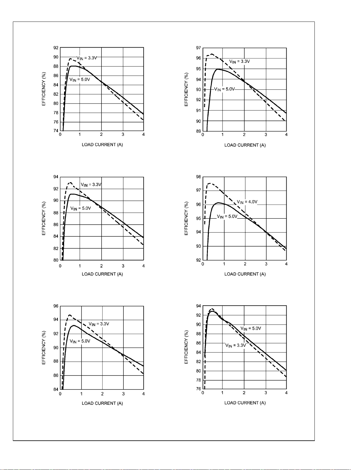
LM2854
LM2854 1 MHz Efficiency vs. I
V
= 0.8V, LO = 0.47 µH, 3.3 mΩ DCR
OUT
LM2854 1 MHz Efficiency vs. I
V
= 1.2V, LO = 0.68 µH, 4.9 mΩ DCR
OUT
OUT
OUT
30052815
LM2854 1 MHz Efficiency vs. I
V
= 2.5V, LO = 1.0 µH, 7.1 mΩ DCR
OUT
LM2854 1 MHz Efficiency vs. I
V
= 3.3V, LO = 1.0 µH, 7.1 mΩ DCR
OUT
OUT
30052816
OUT
LM2854 1 MHz Efficiency vs. I
V
= 1.8V, LO = 1.0 µH, 7.1 mΩ DCR
OUT
OUT
30052817
30052819
30052818
LM2854 500 kHz Efficiency vs. I
V
= 0.8V, LO = 1.0 µH, 7.1 mΩ DCR
OUT
OUT
30052820
7 www.national.com
Page 8

LM2854
LM2854 500 kHz Efficiency vs. I
V
= 2.5V, LO = 2.2 µH, 16 mΩ DCR
OUT
OUT
LM2854 500 kHz Efficiency vs. I
V
= 1.2V, LO = 1.5 µH, 9.7 mΩ DCR
OUT
OUT
LM2854 500 kHz Efficiency vs. I
V
= 3.3V, LO = 1.5 µH, 9.7 mΩ DCR
OUT
LM2854 1 MHz Bode Plot
R
= 150 kΩ, R
FB1
L
OUT
VIN = 3.3V, V
= 0.82 µH, C
= 1.8V, I
OUT
= 1 kΩ, C
COMP
= 100 µF ceramic
OUT
OUT
COMP
30052821
OUT
30052823
= 4A
= 100 pF,
LM2854 500 kHz Efficiency vs. I
V
= 1.8V, LO = 1.5 µH, 9.7 mΩ DCR
OUT
LM2854 500 kHz Bode Plot
R
= 250 kΩ, R
FB1
L
OUT
VIN = 3.3V, V
= 1.5 µH, C
= 1.8V, I
OUT
= 1 kΩ, C
COMP
= 100 µF ceramic
OUT
OUT
COMP
30052822
OUT
30052824
= 4A
= 47 pF,
30052825
www.national.com 8
30052826
Page 9

LM2854
R
= 150 kΩ, R
FB1
R
= 150 kΩ, R
FB1
L
OUT
LM2854 1 MHz Bode Plot
VIN = 5.0V, V
L
= 0.82 µH, C
OUT
OUT
COMP
= 1.8V, I
= 1 kΩ, C
OUT
LM2854 1 MHz Bode Plot
VIN = 5.0V, V
= 0.82 µH, C
= 3.3V, I
OUT
= 1 kΩ, C
COMP
= 100 µF ceramic
OUT
= 4A
OUT
COMP
= 100 µF
= 4A
OUT
COMP
= 100 pF,
30052827
= 68 pF,
R
= 250 kΩ, R
FB1
L
OUT
R
= 250 kΩ, R
FB1
L
OUT
LM2854 500 kHz Bode Plot
VIN = 5.0V, V
= 1.5 µH, C
= 1.8V, I
OUT
= 1 kΩ, C
COMP
= 100 µF ceramic
OUT
LM2854 500 kHz Bode Plot
VIN = 5.0V, V
= 1.5 µH, C
= 3.3V, I
OUT
= 1 kΩ, C
COMP
= 100 µF ceramic
OUT
OUT
COMP
OUT
COMP
= 4A
= 47 pF,
30052828
= 4A
= 33 pF,
LM2854 500 kHz Power On Characteristic
VIN = 5.0V, V
= 1.8V, I
OUT
= 4A, CSS = 220 pF
OUT
30052829
30052831
LM2854 500 kHz Power On via Enable
VIN = 5.0V, V
= 1.8V, I
OUT
= 4A, CSS = 220 pF
OUT
30052830
30052832
9 www.national.com
Page 10

LM2854
LM2854 500 kHz Power Off Characteristic
VIN = 5.0V, V
= 1.8V, I
OUT
= 4A, CSS = 220 pF
OUT
30052833
LM2854 1 MHz Load Transient Response
VIN = 5.0V, V
OUT
= 3.3V, I
= 0.5A to 4A to 0.5A step
OUT
di/dt ≊ 4A/µs, CO = 100 µF ceramic
30052834
LM2854 500 kHz Switch Node Voltage
(oscilloscope set at infinite persistence)
VIN = 5.0V, V
OUT
= 2.5V, I
OUT
= 4A
30052835
LM2854 500 kHz Pre-Biased Startup Waveform
(oscilloscope set at infinite persistence)
V
OUT
= 2.5V, I
OUT
= 0A, V
PRE-BIAS
= 1.25V
LM2854 500 kHz Startup Waveform
V
= 2.5V, I
OUT
OUT
= 0A
30052856
30052855
www.national.com 10
Page 11
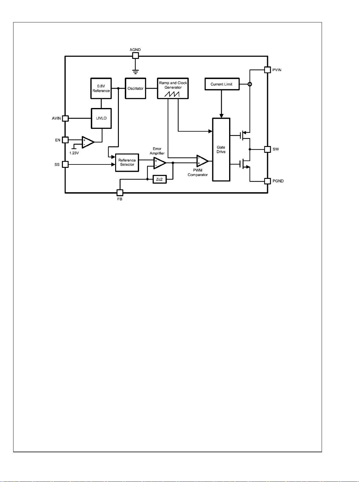
Block Diagram
LM2854
Applications Information
GENERAL
The LM2854 PowerWise® synchronous DC-DC buck regulator belongs to the National Semiconductor SIMPLE
SWITCHER® family of switching regulators. Integration of the
power MOSFETs and associated drivers, compensation component network and the PWM controller reduces the number
of external components necessary for a complete power supply design, without sacrificing performance.
Operation Description
SWITCHING FREQUENCY
The LM2854 is available in two switching frequency options,
500 kHz and 1 MHz. Generally, a higher switching frequency
allows for faster transient response and a reduction in the
footprint area and volume of the external power stage components, while a lower switching frequency affords better
efficiency. These factors should be considered when selecting the appropriate switching frequency for a given application.
ENABLE
The LM2854 features a enable (EN) pin and associated comparator to allow the user to easily sequence the LM2854 from
an external voltage rail, or to manually set the input UVLO
threshold. The turn-on or rising threshold and hysteresis for
this comparator are typically 1.23V and 0.15V respectively.
The precise reference for the enable comparator allows the
user to guarantee that the LM2854 will be disabled when the
system demands it to be.
30052836
spectively. A controlled soft-start eliminates inrush currents
during start-up and allows the user more control and flexibility
when sequencing the LM2854 with other power supplies. An
external soft-start capacitor is used to control the LM2854
start-up time. During soft-start, the voltage on the feedback
pin is connected internally to the non-inverting input of the
error amplifier. The soft-start period lasts until the voltage on
the soft-start pin exceeds the LM2854 reference voltage of
0.8V. At this point, the reference voltage takes over at the noninverting amplifier input.
In the event of either AVIN or EN decreasing below the falling
UVLO or enable threshold respectively, the voltage on the
soft-start pin is collapsed by discharging the soft-start capacitor through a 5 kΩ transistor to ground.
TRACKING
The LM2854 can track the output of a master power supply
during soft-start by connecting a resistor divider to the SS pin.
In this way, the output voltage slew rate of the LM2854 will be
controlled by a master supply for loads that require precise
sequencing. When the tracking function is used, a small value
soft-start capacitor can be connected to the SS pin to alleviate
output voltage overshoot when recovering from a current limit
fault.
SOFT-START
The LM2854 begins to operate when both the AVIN and EN
voltages exceed the rising UVLO and enable thresholds, re-
11 www.national.com
Page 12

LM2854
PRE-BIASED STARTUP CAPABILITY
The LM2854 is in a pre-biased state when the device starts
up with an output voltage greater than zero. This often occurs
in many multi-rail applications such as when powering an FPGA, ASIC, or DSP. The output can be pre-biased in these
applications through parasitic conduction paths from one supply rail to another. Even though the LM2854 is a synchronous
converter, it will not pull the output low when a pre-bias condition exists. The LM2854 will not sink current during start up
until the soft-start voltage exceeds the voltage on the FB pin.
Since the device can not sink current it protects the load from
damage that might otherwise occur if current is conducted
through the parasitic paths of the load.
FEEDBACK VOLTAGE ACCURACY
The FB pin is connected to the inverting input of the voltage
loop error amplifier and during closed loop operation its reference voltage is 0.8V. The FB voltage is accurate to within
-1.25% / +1.0% over temperature. Additionally, the LM2854
contains error nulling circuitry to substantially eliminate the
feedback voltage over temperature drift as well as the long
term aging effects of the internal amplifiers. In addition, the 1/
f noise of the bandgap amplifier and reference are dramatically reduced. The manifestation of this circuit action is that
the duty cycle will have two slightly different but distinct operating points, each evident every other switching cycle. The
oscilloscope plot shown previously of the SW pin with infinite
persistence set shows this behavior. No discernible effect is
evident on the output due to LC filter attenuation. For further
information, a National Semiconductor white paper is available on this topic.
POSITIVE CURRENT LIMIT
The LM2854 employs lossless cycle-by-cycle high-side current limit circuitry to limit the peak current through the highside FET. The peak current limit threshold, denoted ICL, is
nominally set at 6A internally. When a current greater than
ICL is sensed through the PFET, its on-time is immediately
terminated and the NFET is activated. The NFET stays on for
the entire next four switching cycles (effectively four PFET
pulses are skipped). During these skipped pulses, the voltage
on the soft-start pin is reduced by discharging the soft-start
capacitor by a current sink on the soft-start pin of nominally 6
µA or 14 µA for the 500 kHz or 1 MHz options, respectively.
Subsequent over-current events will drain more and more
charge from the soft-start capacitor, effectively decreasing
the reference voltage as the output droops due to the pulse
skipping. Reactivation of the soft-start circuitry ensures that
when the over-current situation is removed, the part will resume normal operation smoothly.
NEGATIVE CURRENT LIMIT
The LM2854 implements negative current limit detection circuitry to prevent large negative current in the inductor. When
30052857
the negative current sensed in the low-side NFET is below
approximately -0.4A, the present switching cycle is immediately terminated and both FETs are turned off. When both
FETs are off, the negative inductor current originally flowing
in the low-side NFET and into the SW pin commutates to the
high-side PFET’s body diode and ramps back to zero. At this
point, the SW pin becomes a high impedance node and ringing can be observed on the SW node as the stored energy in
the inductor is dissipated while resonating with the parasitic
nodal capacitance.
OVER-TEMPERATURE PROTECTION
When the LM2854 senses a junction temperature greater
than 165°C, both switching FETs are turned off and the part
enters a sleep state. Upon sensing a junction temperature
below 155°C, the part will re-initiate the soft-start sequence
and begin switching once again. This feature is provided to
prevent catastrophic failure due to excessive thermal dissipation.
LOOP COMPENSATION
The LM2854 preserves flexibility by integrating the control
components around the error amplifier while utilizing three
small external compensation components from V
An integrated type II (two pole, one zero) voltage-mode com-
OUT
to FB.
pensation network is featured. To ensure stability, an external
resistor and small value capacitor can be added across the
upper feedback resistor as a pole-zero pair to complete a type
III (three pole, two zero) compensation network. For correct
selection of these components, see the design section of this
datasheet.
Design Guidelines
INPUT FILTER CAPACITOR
Fast switching currents place a large strain on the input supply
to a buck regulator. A capacitor placed close to the PVIN and
PGND pins of the LM2854 helps to supply the instantaneous
charge required when the regulator demands a pulse of current every switching cycle. In fact, the input capacitor conducts a square-wave current of peak-to-peak amplitude equal
to I
. With this high AC current present in the input capac-
OUT
itor, the RMS current rating becomes an important parameter.
The necessary RMS current rating of the input capacitor to a
buck regulator can be estimated by
where the PWM duty cycle, D, is given by
Neglecting capacitor ESR, the resultant input capacitor AC
ripple voltage is a triangular waveform with peak-to-peak amplitude specified as follows
The maximum input capacitor ripple voltage and RMS current
occur at 50% duty cycle. A 22 µF or 47 µF high quality dielectric (X5R, X7R) ceramic capacitor with adequate voltage
rating is typically sufficient as an input capacitor to the
www.national.com 12
Page 13

LM2854. The input capacitor should be placed as close as
possible to the PVIN and PGND pins to substantially eliminate
the parasitic effects of any stray inductance or resistance on
the PC board and supply lines. Additional bulk capacitance
with higher ESR may be required to damp any resonance effects of the input capacitance and parasitic inductance.
AVIN FILTERING COMPONENTS
In addition to the large input filter capacitor, a smaller ceramic
capacitor such as a 0.1 µF or 1.0 µF is recommended between
AVIN and AGND to filter high frequency noise present on the
PVIN rail from the quiet AVIN supply. For additional filtering
in noisy environments, a small RC filter can be used on the
AVIN pin as shown below.
30052840
In general, RF is typically selected between 1Ω and 10Ω so
that the steady state voltage drop across the resistor due to
the AVIN bias current does not affect the UVLO level. Recommended filter capacitor, CF, is 1.0 µF in X5R or X7R
dielectric.
The above equation includes an offset voltage to ensure that
the final value of the SS pin voltage exceeds the reference
voltage of the LM2854. This offset will cause the LM2854 output voltage to reach regulation slightly before the master
supply. A value of 33 kΩ 1% is recommended for RT2 as a
compromise between high precision and low quiescent current through the divider while minimizing the effect of the 2 µA
soft-start current source.
For example, If the master supply voltage V
the LM2854 output voltage was 1.8V, then the value of R
is 3.3V and
OUT1
needed to give the two supplies identical soft-start times
would be 14.3 kΩ. A timing diagram for this example, the
equal soft-start time case, is shown below.
LM2854
T1
SOFT-START CAPACITOR
When the LM2854 is enabled, the output voltage will ramp up
linearly in the time dictated by the following relationship
where V
ISS is the soft-start charging current (nominally 2 µA) and
is the internal reference voltage (nominally 0.8V),
REF
CSS is the external soft-start capacitance. Rearranging this
equation allows for the necessary soft-start capacitor for a
given startup time to be calculated as follows
Thus, the required soft start capacitor per unit output voltage
startup time is given by
CSS = 2.5 nF / ms
For example, a 10 nF soft-start capacitor will yield a 4 ms softstart time.
TRACKING - EQUAL SOFT-START TIME
One way to use the tracking feature is to design the tracking
resistor divider so that the master supply output voltage,
V
, and the LM2854 output voltage, V
OUT1
gether and reach their target values at the same time. This is
, both rise to-
OUT2
termed ratiometric startup. For this case, the equation governing the values of tracking divider resistors RT1 and RT2 is
given by
30052859
TRACKING - EQUAL SLEW RATES
Alternatively, the tracking feature can be used to have similar
output voltage ramp rates. This is referred to as simultaneous
startup. In this case, the tracking resistors can be determined
based on the following equation
and to ensure proper overdrive of the SS pin
V
< 0.8 V
OUT2
For the example case of V
RT2 set to 33 kΩ as before, RT1 is calculated from the above
= 5V and V
OUT1
OUT1
= 2.5V, with
OUT2
equation to be 15.5 kΩ. A timing diagram for the case of equal
slew rates is shown below.
13 www.national.com
Page 14

LM2854
ENABLE AND UVLO
Using a resistor divider from VIN to EN as shown in the
schematic diagram below, the input voltage at which the part
begins switching can be increased above the normal input
UVLO level according to
For example, suppose that the required input UVLO level is
3.69V. Choosing R
kΩ.
= 10 kΩ, then we calculate R
EN2
30052861
EN1
= 20
R
is defined based on the voltage loop requirements and
FB1
R
is then selected for the desired output voltage. These
FB2
resistors are normally selected as 0.5% or 1% tolerance.
COMPENSATION COMPONENT SELECTION
The power stage transfer function of a voltage mode buck
converter has a complex double pole related to the LC output
filter and a left half plane zero due to the output capacitor
ESR, denoted R
given respectively by
. The locations of these singularities are
ESR
where CO is the output capacitance value appropriately derated for applied voltage and operating temperature, RL is the
effective load resistance and R
sistance associated with the inductor and power switches.
is the series damping re-
DCR
30052844
Alternatively, the EN pin can be driven from another voltage
source to cater for system sequencing requirements commonly found in FPGA and other multi-rail applications. The
following schematic shows an LM2854 that is sequenced to
start based on the voltage level of a master system rail.
30052845
OUTPUT VOLTAGE SETTING
A divider resistor network from V
the desired output voltage as follows
www.national.com 14
to the FB pin determines
OUT
30052848
The conventional compensation strategy employed with voltage mode control is to use two compensator zeros to offset
the LC double pole, one compensator pole located to cancel
the output capacitor ESR zero and one compensator pole located between one third and one half switching frequency for
high frequency noise attenuation.
The LM2854 internal compensation components are designed to locate a pole at the origin and a pole at high
frequency as mentioned above. Furthermore, a zero is located at 8.8 kHz or 17.6 kHz for the 500 kHz or 1 MHz options,
respectively, to approximately cancel the likely location of one
LC filter pole.
The three external compensation components, R
and C
pole location and a pole to cancel the ESR zero. The voltage
loop crossover frequency, f
one tenth to one fifth of the switching frequency
, are selected to position a zero at or below the LC
COMP
, is usually selected between
loop
0.1fSW ≤ f
loop
≤ 0.2f
SW
FB1
, R
COMP
A simple solution for the required external compensation capacitor, C
expressed as
, with type III voltage mode control can be
COMP
Page 15

where the constant α is nominally 0.038 or 0.075 for the 500
kHz or 1 MHz options, respectively. This assumes a compensator pole cancels the output capacitor ESR zero. Furthermore, since the modulator gain is proportional to VIN, the
loop crossover frequency increases with VIN. Thus, it is recommended to design the loop at maximum expected VIN.
The upper feedback resistor, R
equate mid-band gain and to locate a zero at or below the LC
pole frequency. The series resistor, R
cate a pole at the ESR zero frequency. Thus
Note that the lower feedback resistor, R
the control loop from an AC standpoint since the FB pin is the
, is selected to provide ad-
FB1
, is selected to lo-
COMP
, has no impact on
FB2
input to an error amplifier and effectively at AC ground.
Hence, the control loop can be designed irrespective of output
voltage level. The only caveat here is the necessary derating
of the output capacitance with applied voltage. Having chosen
R
as above, R
FB1
voltage.
is then selected for the desired output
FB2
Table 1 and Table 2 list inductor and ranges of capacitor values that work well with the LM2854, along with the associated
compensation components to ensure stable operation. Values different than those listed may be used, but the compensation components may need to be recalculated to avoid
degradation in phase margin. Note that the capacitance
ranges specified refer to in-circuit values where the nominal
capacitance value is adequately derated for applied voltage.
FILTER INDUCTOR AND OUTPUT CAPACITOR SELECTION
In a buck regulator, selection of the filter inductor and capacitor will affect many key system parameters, including stability, transient response and efficiency The LM2854 can
accommodate relatively wide ranges of output capacitor and
filter inductor values in a typical application and still achieve
excellent load current transient performance and low output
voltage ripple.
The inductance is chosen such that the peak-to-peak inductor
current ripple, ΔiL, is approximately 25 to 40% of I
lows
OUT
as fol-
Note that the peak inductor current is the DC output current
plus half the ripple current and reaches its highest level at
lowest duty cycle (or highest VIN). It is recommended that the
inductor should have a saturation current rating in excess of
the current limit level.
Table 3 lists examples of off-the-shelf powdered iron and ferrite based inductors that are suitable for use with the LM2854.
The output capacitor can be of ceramic or electrolytic chemistry. The chosen output capacitor requires sufficient DC voltage rating and RMS ripple current handling capability.
The output capacitor RMS current and peak-to-peak output
ripple are given respectively by
In general, 22 µF to 100 µF of ceramic output capacitance is
sufficient for both LM2854 frequency options given the optimal high frequency characteristics and low ESR of ceramic
dielectric. It is advisable to consult the manufacturer’s derating curves for capacitance voltage coefficient as the in-circuit
capacitance may drop significantly with applied voltage.
Tantalum or organic polymer electrolytic capacitance may be
suitable with the LM2854 500 kHz option, particularly in applications where substantial bulk capacitance per unit volume
is required. However, the high loop bandwidth achievable with
the LM2854 obviates the necessity for large bulk capacitance
during transient loading conditions.
Table 4 lists some examples of commercially available capacitors that can be used with the LM2854.
LM2854
TABLE 1. LM2854 500 kHz Compensation Component Values
VIN (V) LO (µH) CO (µF)
ESR (mΩ) R
FB1
(kΩ)
C
COMP
(pF)
R
Min Max Min Max
5.0 1.5 40 100 2 10 150 47 1
1.5 100 200 1 5 150 100 1
1.5 100 220 15 25 150 120 25
2.2 40 100 2 10 150 68 1
2.2 100 200 1 5 150 120 1
2.2 100 220 15 25 120 120 15
3.3 1.5 40 100 2 10 150 68 1
1.5 100 200 1 5 100 150 1
1.5 100 220 15 25 100 150 15
2.2 40 100 2 10 150 100 1
2.2 100 200 1 5 100 220 1
2.2 100 220 15 25 100 220 10
15 www.national.com
COMP
(kΩ)
Page 16

TABLE 2. LM2854 1 MHz Compensation Component Values
LM2854
VIN (V) LO (µH) CO (µF)
ESR (mΩ) R
FB1
(kΩ)
C
COMP
(pF)
Min Max Min Max
5.0 0.68 20 60 2 10 120 33 1
0.68 60 150 1 5 75 100 1
0.68 100 220 15 25 100 100 20
1.0 20 60 2 10 100 56 1
1.0 60 150 1 5 75 150 1
1.0 100 220 15 25 75 150 15
3.3 0.68 20 60 2 10 75 56 1
0.68 60 150 1 5 50 150 1
0.68 100 220 15 25 50 150 12
1.0 20 60 2 10 75 82 1
1.0 60 150 1 5 50 220 1
1.0 100 220 15 25 33 330 10
TABLE 3. Recommended Filter Inductors
R
COMP
(kΩ)
Inductance (µH)
DCR (mΩ)
Manufacturer Manufacturer P/N Case Size (mm)
0.47 14.5 Vishay Dale IHLP1616BZERR47M11 4.06 x 4.45 x 2.00
1.0 24.0 Vishay Dale IHLP1616BZER1R0M11 4.06 x 4.45 x 2.00
0.47 8.4 Vishay Dale IHLP2525AHERR47M01 6.47 x 6.86 x 1.80
0.47 6.0 Vishay Dale IHLP2525BDERR47M01 6.47 x 6.86 x 2.40
0.68 8.7 Vishay Dale IHLP2525BDERR68M01 6.47 x 6.86 x 2.40
0.82 10.6 Vishay Dale IHLP2525BDERR82M01 6.47 x 6.86 x 2.40
1.0 13.1 Vishay Dale IHLP2525BDER1R0M01 6.47 x 6.86 x 2.40
1.5 18.5 Vishay Dale IHLP2525BDER1R5M01 6.47 x 6.86 x 2.40
2.2 15.7 Vishay Dale IHLP2525CZER2R2M11 6.47 x 6.86 x 3.00
0.47 3.5 Sumida CDMC6D28NP-R47M 6.50 x 7.25 x 3.00
0.68 4.5 Sumida CDMC6D28NP-R68M 6.50 x 7.25 x 3.00
1.0 17.3 Sumida CDMC6D28NP-1R0M 6.50 x 7.25 x 3.00
1.5 10.4 Sumida CDMC6D28NP-1R5M 6.50 x 7.25 x 3.00
2.2 16.1 Sumida CDMC6D28NP-2R2M 6.50 x 7.25 x 3.00
0.56 10 Coilcraft DO1813H-561ML 6.10 x 8.89 x 5.00
0.47 3.3 Coilcraft HA3619-471ALC 7.0 x 7.0 x 3.0
0.68 4.8 Coilcraft HA3619-681ALC 7.0 x 7.0 x 3.0
1.0 7.5 Coilcraft HA3619-102ALC 7.0 x 7.0 x 3.0
1.2 9.4 Coilcraft HA3619-122ALC 7.0 x 7.0 x 3.0
1.5 11.5 Coilcraft HA3619-152ALC 7.0 x 7.0 x 3.0
1.8 16.5 Coilcraft HA3619-182ALC 7.0 x 7.0 x 3.0
0.47 3.3 TDK SPM6530T-R47M170 7.1 x 6.5 x 3.0
0.68 4.9 TDK SPM6530T-R68M140 7.1 x 6.5 x 3.0
1.0 7.1 TDK SPM6530T-1R0M120 7.1 x 6.5 x 3.0
1.5 9.7 TDK SPM6530T-1R5M100 7.1 x 6.5 x 3.0
0.47 14 Cyntec PCMC042T-0R47MN 4.0 x 4.5 x 2.0
1.0 9 Cyntec PCMC063T-1R0MN 6.5 x 6.9 x 3.0
1.5 14 Cyntec PCMC063T-1R5MN 6.5 x 6.9 x 3.0
www.national.com 16
Page 17
TABLE 4. Recommended Filter Capacitors
LM2854
Capacitance
(µF)
22 6.3, < 5 Ceramic, X5R TDK C3216X5R0J226M 1206
47 6.3, < 5 Ceramic, X5R TDK C3216X5R0J476M 1206
47 6.3, < 5 Ceramic, X5R TDK C3225X5R0J476M 1210
47 10.0, < 5 Ceramic, X5R TDK C3225X5R1A476M 1210
100 6.3, < 5 Ceramic, X5R TDK C3225X5R0J107M 1210
100 6.3, 50 Tantalum AVX TPSD157M006#0050 D, 7.5 x 4.3 x 2.9 mm
100 6.3, 25 Organic Polymer Sanyo 6TPE100MPB2 B2, 3.5 x 2.8 x 1.9 mm
150 6.3, 18 Organic Polymer Sanyo 6TPE150MIC2 C2, 6.0 x 3.2 x 1.8 mm
330 6.3, 18 Organic Polymer Sanyo 6TPE330MIL D3L, 7.3 x 4.3 x 2.8 mm
470 6.3, 23 Niobium Oxide AVX NOME37M006#0023 E, 7.3 x 4.3 x 4.1 mm
Voltage (V), ESR
(mΩ)
Chemistry Manufacturer Manufacturer P/N Case Size
17 www.national.com
Page 18
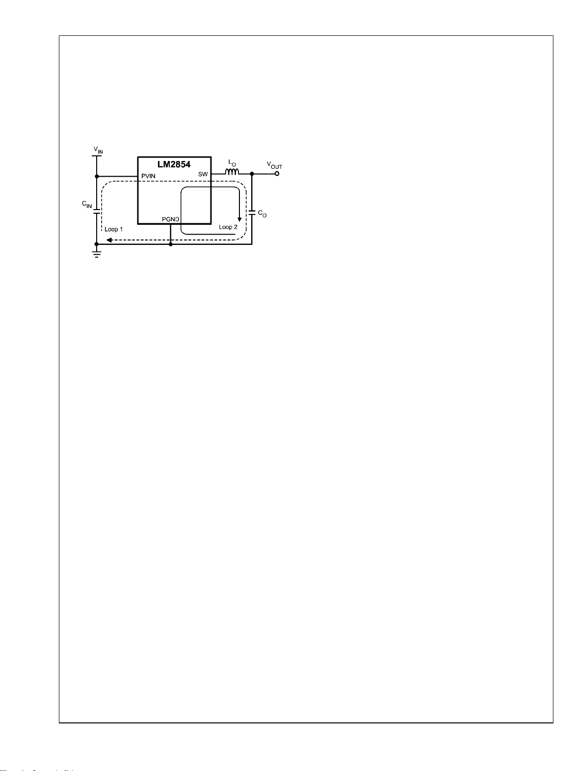
PC Board Layout Guidelines
PC board layout is an important part of DC-DC converter de-
LM2854
sign. Poor board layout can disrupt the performance of a DCDC converter and surrounding circuitry by contributing to EMI,
ground bounce and resistive voltage drop in the traces. These
can send erroneous signals to the DC-DC converter resulting
in poor regulation or instability. Good layout can be implemented by following a few simple design rules.
1. Minimize area of switched current loops.
There are two loops where currents are switched at high di/
dt slew rates in a buck regulator. The first loop represents the
path taken by AC current flowing during the high side PFET
on time. This current flows from the input capacitor to the regulator PVIN pins, through the high side FET to the regulator
SW pin, filter inductor, output capacitor and returning via the
PCB ground plane to the input capacitor.
The second loop represents the path taken by AC current
flowing during the low side NFET on time. This current flows
from the output capacitor ground to the regulator PGND pins,
through the NFET to the inductor and output capacitor. From
an EMI reduction standpoint, it is imperative to minimize this
loop area during PC board layout by physically locating the
input capacitor close to the LM2854. Specifically, it is advantageous to place CIN as close as possible to the LM2854 PVIN
and PGND pins. Grounding for both the input and output capacitor should consist of a localized top side plane that connects to PGND and the exposed die attach pad (DAP). The
inductor should be placed close to the SW pin and output capacitor.
30052853
2. Minimize the copper area of the switch node.
The LM2854 has two SW pins optimally located on one side
of the package. In general the SW pins should be connected
to the filter inductor on the top PCB layer. The inductor should
be placed close to the SW pins to minimize the copper area
of the switch node.
3. Have a single point ground for all device analog
grounds located under the DAP.
The ground connections for the Feedback, Soft-start, Enable
and AVIN components should be routed to the AGND pin of
the device. The AGND pin should connect to PGND under the
DAP. This prevents any switched or load currents from flowing in the analog ground traces. If not properly handled, poor
grounding can result in degraded load regulation or erratic
switching behavior.
4. Minimize trace length to the FB pin.
Since the feedback (FB) node is high impedance, the trace
from the output voltage setpoint resistor divider to FB pin
should be as short as possible. This is most important as relatively high value resistors are used to set the output voltage.
The FB trace should be routed away from the SW pin and
inductor to avoid noise pickup from the SW pin. Both feedback
resistors, R
R
COMP
and C
FB1
and R
COMP
, and the compensation components,
FB2
, should be located close to the FB pin.
5. Make input and output bus connections as wide as
possible.
This reduces any voltage drops on the input or output of the
converter and maximizes efficiency. To optimize voltage accuracy at the load, ensure that a separate feedback voltage
sense trace is made to the load. Doing so will correct for voltage drops and provide optimum output accuracy.
6. Provide adequate device heat-sinking.
Use an array of heat-sinking vias to connect the DAP to the
ground plane on the bottom PCB layer. If the PCB has a plurality of copper layers, these thermal vias can also be employed to make connection to inner layer heat-spreading
ground planes. For best results use a 5 x 3 via array with
minimum via diameter of 10 mils. Ensure enough copper area
is used to keep the junction temperature below 125°C.
www.national.com 18
Page 19

LM2854 Application Circuit Schematic and BOMs
This section provides several application solutions with an
associated bill of materials. All bill of materials reference the
schematic below. The compensation for each solution was
optimized to work over the full input range. Many applications
have a fixed input voltage rail. It is possible to modify the
compensation to obtain a faster transient response for a given
input voltage operating point.
LM2854
30052854
TABLE 5. LM2854 500kHz Bill of Materials, VIN = 5V, V
= 3.3V, I
OUT
OUT(MAX)
= 4A, Optimized for Efficiency
Ref Des Description Case Size Manufacturer Manufacturer P/N
U1 Synchronous Buck
eTSSOP-16 National Semiconductor LM2854MHX-500
Regulator
R
R
R
C
C
IN
C
O
L
O
FB1
FB2
COMP
R
F
COMP
C
SS
C
F
47 µF, X5R, 10V 1210 TDK C3225X5R1A476M
100 µF, X5R, 6.3V 1210 TDK C3225X5R0J107M
1.5 µH, 9.7 mΩ, 10A
249 kΩ
80.6 kΩ
1.0 kΩ
1.0Ω
7.1 x 6.5 x 3.0 mm TDK SPM6530T-1R5M100
0603 Vishay Dale CRCW06032493F-e3
0603 Vishay Dale CRCW060328062F-e3
0603 Vishay Dale CRCW06031001F-e3
0603 Vishay Dale CRCW06031R0F-e3
33 pF, ±5%, C0G, 50V 0603 TDK C1608C0G1H330J
10 nF, ±10%, X7R, 16V 0603 Murata GRM188R71C103KA01
1.0 µF, ±10%, X7R, 10V 0603 Murata GRM188R71A105KA61
19 www.national.com
Page 20

TABLE 6. LM2854 1 MHz Bill of Materials, VIN = 3.3V to 5V, V
LM2854
Ref Des Description Case Size Manufacturer Manufacturer P/N
U1 Synchronous Buck Regulator eTSSOP-16 National Semiconductor LM2854MHX-1000
R
R
R
C
C
IN
C
O
L
O
FB1
FB2
COMP
R
F
COMP
C
SS
C
F
150 µF, 6.3V, 18 mΩ
330 µF, 6.3V, 18 mΩ
2.2 µH, 16 mΩ, 7A
100 kΩ
47.5 kΩ
15 kΩ
1.0Ω
330 pF, ±5%, C0G, 50V 0603 TDK C1608C0G1H331J
10 nF, ±10%, X7R, 16V 0603 Murata GRM188R71C103KA01
1.0 µF,±10%, X7R, 10V 0603 Murata GRM188R71A105KA61
= 2.5V, I
Output Capacitance
OUT
OUT (MAX)
= 4A, Optimized for Electrolytic Input and
C2, 6.0 x 3.2 x 1.8 mm Sanyo 6TPE150MIC2
D3L, 7.3 x 4.3 x 2.8 mm Sanyo 6TPE330MIL
6.47 x 6.86 x 3.00 mm Vishay Dale IHLP2525CZER2R2M11
0603 Vishay Dale CRCW06031003F-e3
0603 Vishay Dale CRCW060324752F-e3
0603 Vishay Dale CRCW06031502F-e3
0603 Vishay Dale CRCW06031R0F-e3
TABLE 7. LM2854 1 MHz Bill of Materials, VIN = 3.3V, V
= 0.8V, I
OUT
Response
OUT (MAX)
= 4A, Optimized for Solution Size and Transient
Ref Des Description Case Size Manufacturer Manufacturer P/N
U1 Synchronous Buck Regulator eTSSOP-16 National Semiconductor LM2854MHX-1000
R
C
C
C
L
R
FB1
COMP
R
COMP
C
SS
C
IN
O
O
F
F
47 µF, X5R, 6.3V 1206 TDK C3216X5R0J476M
47 µF, X5R, 6.3V 1206 TDK C3216X5R0J476M
0.47 µH, 14.5 mΩ, 7A
110 kΩ
1.0 kΩ
1.0Ω
4.06 x 4.45 x 2.00 mm Vishay Dale IHLP1616BZER0R47M11
0402 Vishay Dale CRCW04021103F-e3
0402 Vishay Dale CRCW04021001F-e3
0402 Vishay Dale CRCW04021R0F-e3
27 pF, ±5%, C0G, 50V 0402 Murata GRM1555C1H270JZ01
10 nF, ±10%, X7R, 16V 0402 Murata GRM155R71C103KA01
1.0 µF, ±10%, X7R, 10V 0402 Murata GRM155R61A105KE15
www.national.com 20
Page 21

Physical Dimensions inches (millimeters) unless otherwise noted
LM2854
16-Lead eTSSOP Package
NS Package Number MXA16A
21 www.national.com
Page 22

Notes
For more National Semiconductor product information and proven design tools, visit the following Web sites at:
Products Design Support
Amplifiers www.national.com/amplifiers WEBENCH www.national.com/webench
Audio www.national.com/audio Analog University www.national.com/AU
Clock Conditioners www.national.com/timing App Notes www.national.com/appnotes
Data Converters www.national.com/adc Distributors www.national.com/contacts
Displays www.national.com/displays Green Compliance www.national.com/quality/green
Ethernet www.national.com/ethernet Packaging www.national.com/packaging
Interface www.national.com/interface Quality and Reliability www.national.com/quality
LVDS www.national.com/lvds Reference Designs www.national.com/refdesigns
Power Management www.national.com/power Feedback www.national.com/feedback
Switching Regulators www.national.com/switchers
LDOs www.national.com/ldo
LED Lighting www.national.com/led
PowerWise www.national.com/powerwise
Serial Digital Interface (SDI) www.national.com/sdi
Temperature Sensors www.national.com/tempsensors
Wireless (PLL/VCO) www.national.com/wireless
THE CONTENTS OF THIS DOCUMENT ARE PROVIDED IN CONNECTION WITH NATIONAL SEMICONDUCTOR CORPORATION
(“NATIONAL”) PRODUCTS. NATIONAL MAKES NO REPRESENTATIONS OR WARRANTIES WITH RESPECT TO THE ACCURACY
OR COMPLETENESS OF THE CONTENTS OF THIS PUBLICATION AND RESERVES THE RIGHT TO MAKE CHANGES TO
SPECIFICATIONS AND PRODUCT DESCRIPTIONS AT ANY TIME WITHOUT NOTICE. NO LICENSE, WHETHER EXPRESS,
IMPLIED, ARISING BY ESTOPPEL OR OTHERWISE, TO ANY INTELLECTUAL PROPERTY RIGHTS IS GRANTED BY THIS
DOCUMENT.
TESTING AND OTHER QUALITY CONTROLS ARE USED TO THE EXTENT NATIONAL DEEMS NECESSARY TO SUPPORT
NATIONAL’S PRODUCT WARRANTY. EXCEPT WHERE MANDATED BY GOVERNMENT REQUIREMENTS, TESTING OF ALL
PARAMETERS OF EACH PRODUCT IS NOT NECESSARILY PERFORMED. NATIONAL ASSUMES NO LIABILITY FOR
APPLICATIONS ASSISTANCE OR BUYER PRODUCT DESIGN. BUYERS ARE RESPONSIBLE FOR THEIR PRODUCTS AND
APPLICATIONS USING NATIONAL COMPONENTS. PRIOR TO USING OR DISTRIBUTING ANY PRODUCTS THAT INCLUDE
NATIONAL COMPONENTS, BUYERS SHOULD PROVIDE ADEQUATE DESIGN, TESTING AND OPERATING SAFEGUARDS.
EXCEPT AS PROVIDED IN NATIONAL’S TERMS AND CONDITIONS OF SALE FOR SUCH PRODUCTS, NATIONAL ASSUMES NO
LIABILITY WHATSOEVER, AND NATIONAL DISCLAIMS ANY EXPRESS OR IMPLIED WARRANTY RELATING TO THE SALE
AND/OR USE OF NATIONAL PRODUCTS INCLUDING LIABILITY OR WARRANTIES RELATING TO FITNESS FOR A PARTICULAR
PURPOSE, MERCHANTABILITY, OR INFRINGEMENT OF ANY PATENT, COPYRIGHT OR OTHER INTELLECTUAL PROPERTY
RIGHT.
LIFE SUPPORT POLICY
NATIONAL’S PRODUCTS ARE NOT AUTHORIZED FOR USE AS CRITICAL COMPONENTS IN LIFE SUPPORT DEVICES OR
SYSTEMS WITHOUT THE EXPRESS PRIOR WRITTEN APPROVAL OF THE CHIEF EXECUTIVE OFFICER AND GENERAL
COUNSEL OF NATIONAL SEMICONDUCTOR CORPORATION. As used herein:
Life support devices or systems are devices which (a) are intended for surgical implant into the body, or (b) support or sustain life and
whose failure to perform when properly used in accordance with instructions for use provided in the labeling can be reasonably expected
to result in a significant injury to the user. A critical component is any component in a life support device or system whose failure to perform
can be reasonably expected to cause the failure of the life support device or system or to affect its safety or effectiveness.
National Semiconductor and the National Semiconductor logo are registered trademarks of National Semiconductor Corporation. All other
brand or product names may be trademarks or registered trademarks of their respective holders.
Copyright© 2008 National Semiconductor Corporation
For the most current product information visit us at www.national.com
National Semiconductor
Americas Technical
Support Center
Email:
LM2854 4A 500 kHz / 1 MHz PowerWise® Synchronous SIMPLE SWITCHER® Buck Regulator
www.national.com
new.feedback@nsc.com
Tel: 1-800-272-9959
National Semiconductor Europe
Technical Support Center
Email: europe.support@nsc.com
German Tel: +49 (0) 180 5010 771
English Tel: +44 (0) 870 850 4288
National Semiconductor Asia
Pacific Technical Support Center
Email: ap.support@nsc.com
National Semiconductor Japan
Technical Support Center
Email: jpn.feedback@nsc.com
 Loading...